5. Electronics production
Group assignment
- Characterize the design rules for your PCB production process
Individual assignment
- Make an in-circuit programmer by milling the PCB, program it, then optionally, trying other processes.
Learning outcomes
- Described the process of milling, stuffing, de-bugging and programming
- Demonstrate correct workflows and identify areas for improvement if required
Have you?
- Shown how you made and programmed the board
- Explained any problems and how you fixed them
- Included a ‘hero shot’ of your board
Group assignment
Our group: Lucasz, Gleb, Perttu and I.
PCB milling
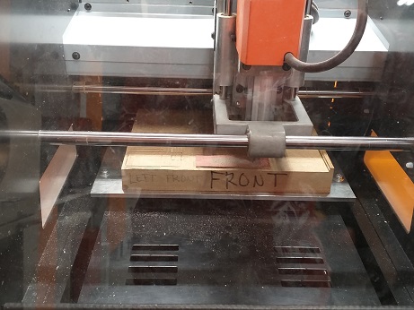
For PCB milling we used Roland SRM-20 Desktop Milling Machine.
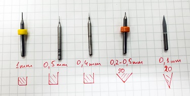
We wanted to test different size bits to see what would be the best for the individual PCB milling. We used the test desing that was available in Electronics production page.
First we cut the PCB into smaller parts, since big plate is easily bent and the result will be uneven.
We also checked that the plate surface of the milling machine is straight, otherwise it will be a problem when using v-bit.
Next we taped the PCB bottom side so that it can be properly attached to the milling plate.
Then we attached the bit to the milling machine. Bits need to be handled very carefully.
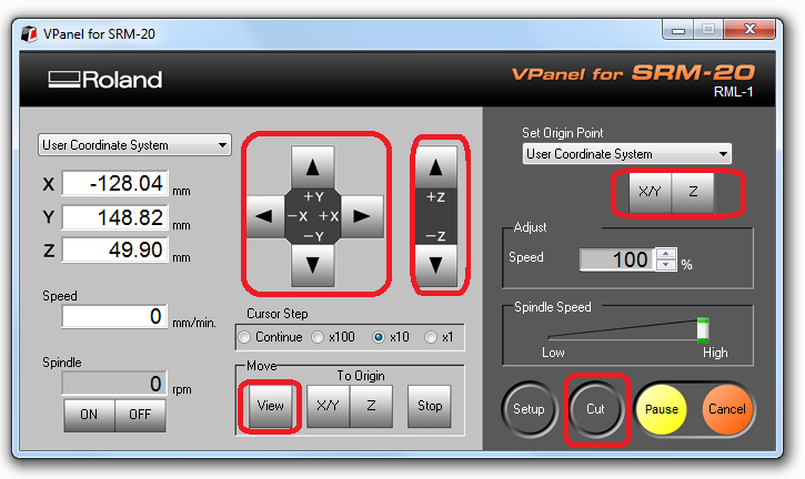
For the milling bit change, you can use “View” button in VPanel. This moves the head to the View position, that is the left end in the highest position for the spindle head, and the front most position for the table.
The starting position (origin) and the cut depth needs to be carefully defined using the Roland VPanel x-, y- and z-axe buttons. X- axis moves the table, and and Y- and Z-axes move the head.
Move the axes manually by the VPanel arrows with suitable Cursor Step. “Continue” moves as long as you push it, use this to move X and Y near to the aimed origin. “x100” and “x10” do smaller steps to get closer. Never use “Continue” with Z-axe!
Adjust X- and Y-axes (with the Cursor Step “Continue” and “x100”) and reset them to be a new origin by Set Origin Point and pressing X/Y.
Move the Z-axe carefully near to the surface. Remember to move Z-axe very slowly, so that you won’t break the bit by letting the bit crash to the surface! When Z-axe is close to surface, loosen and lower the bit by hand, don’t let it fall down! Lower the bit to the surface and fasten it there to get z-zero directly to the material top. Bits are breaking very easily, so be very careful with them!
Reset the Z-axis to be zero by Set Origin Point and pressing Z. In order to let the milling bit turn on and speed up freely, move the Z-axis just a little bit up (around 5 steps with the x10) so that the milling bit is not left directly on the surface. Now the machine preparation is done and you can press “Cut” to open Output File List to select the milling file. But let’s prepare the milling file first in mod (unless this is done earlier).
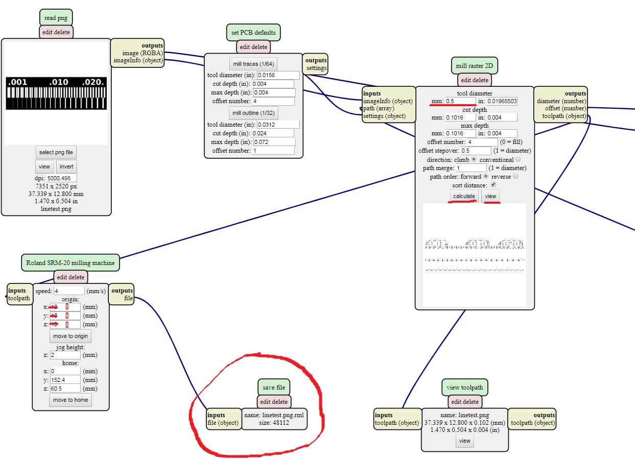
The design file can be defined using mod. Right click on the window and select “programs/open server program/SRM-20(PCB)”. Select your png file. Next delete WebSocket device module and right click on the window and select “modules/open server module/file (save)”. Then set origin coordinates (x, y, z) to (0,0,0) and connect output Roland SRM-20 milling machine and input save file. Open your png file in read png module. Define tool diameter and cut depth in mill raster 2D module and press calculate. testlines.rml is created. Click “view” button to check if the created path is correct.
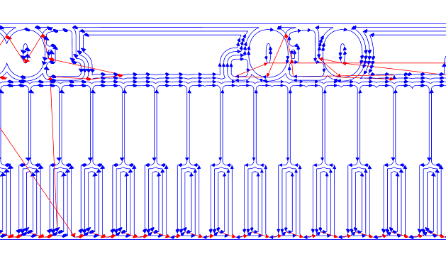
In VPanel press “Cut” button and Select “Delete All” from the Output file list. Press “Add” to add your milling file testlines.rml and open it. Press Output-button, milling starts.
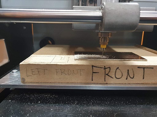
When milling is done, open the door and clean the plate with vacuum cleaner.
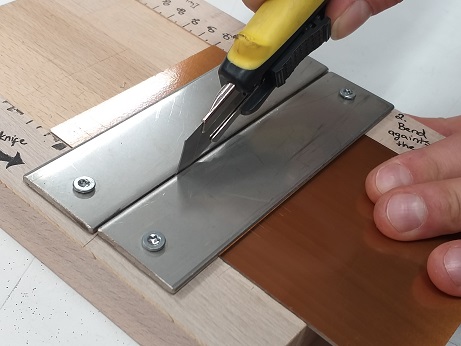
Now we need to cut the outline. interior -file is used for that. The process is similar than with traces. Milling bit needs to be changed to 1mm bit for that.
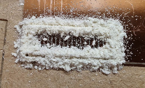
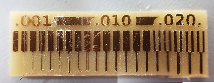
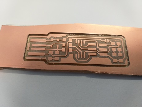
We can compare the milled test PCBs with the linetest png:

Here is the first test PCB milled with 0,5 mm bit.
Thinnest spacing is 16 mil and thinnest trace is 10 mil.
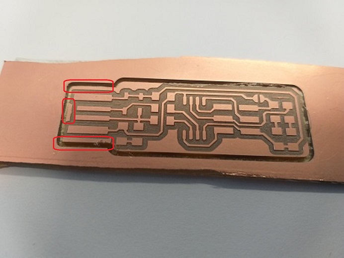
Here is 0,2-0,5 mm v-shaped bit test PCB
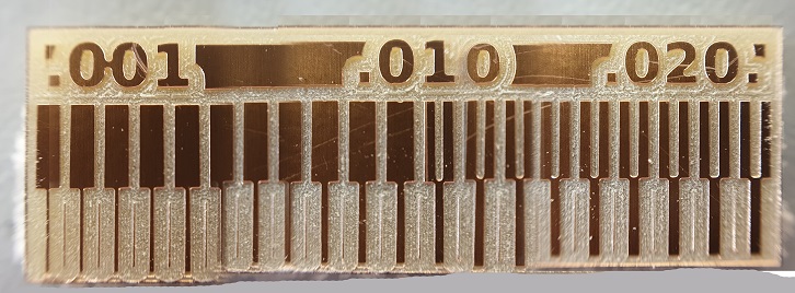
Thinnest spacing is 12 mil and thinnest trace is 1 mil.
Individual assignment
I am following the instructions created by Brian.
PCB fabrication
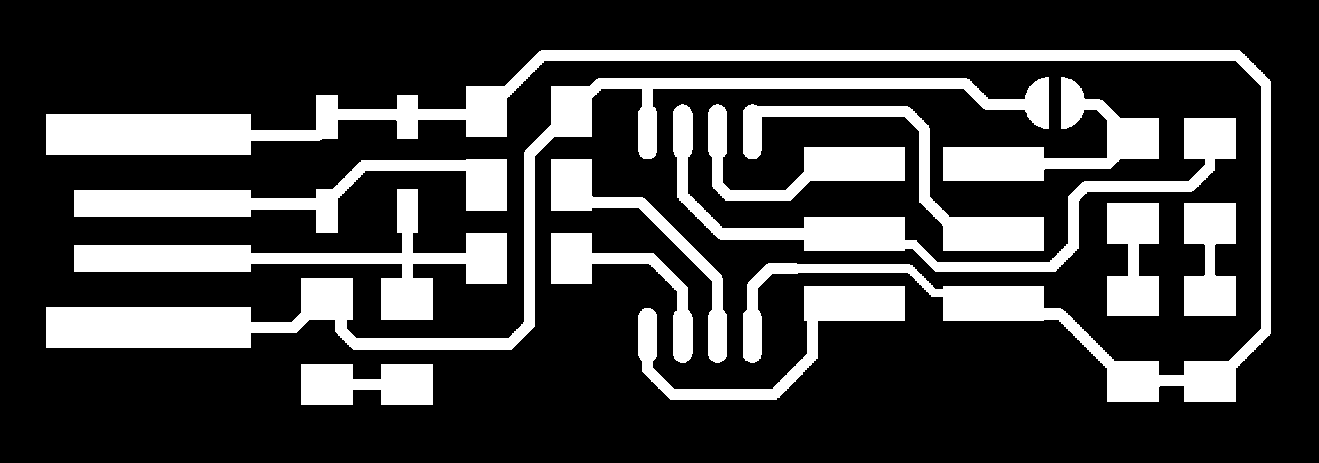
I downloaded the PNG files for the traces and the board outline:
Traces (1000 dpi)
Outline Cutout (1000 dpi)
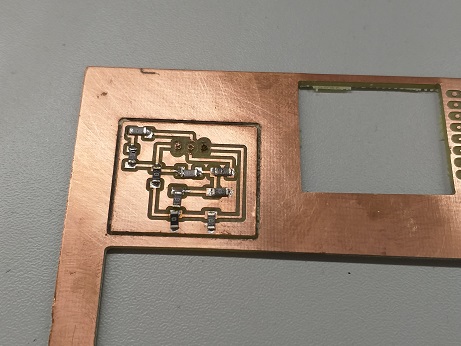
I used the milling process described in the previous chapter. I used 0.2-0.5 mm v-shape bit for traces cutting.

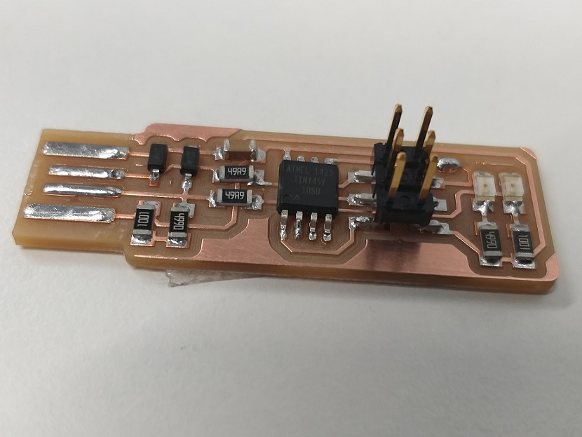
Here is the milled PCB I created:
The extra copper in the front was removed with a knife.
Before soldering the PCB board I did some practicing, because the soldering is new to me.
Assembling the PCB
When I was happy with practicing, I started to work with the actual PCB board. First I brushed the surface with steel wool to clean it, to assure good soldering results. After that I started the soldering under a microscope.
Here is the list of needed parts:
- 1x ATtiny45 or ATtiny85
- 2x 1kΩ resistors
- 2x 499Ω resistors
- 2x 49Ω resistors
- 2x 3.3v zener diodes
- 1x red LED
- 1x green LED
- 1x 100nF capacitor
- 1x 2x3 pin header
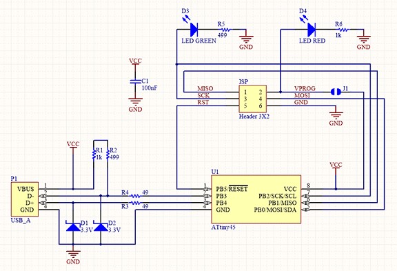
I was soldering the parts to the PCB, using the schematic and board image below as a reference for component values and placement. I started with the most difficult parts (the ATtiny45) first, so I had the most access. I installed the ISP header last, as it is large and can get in the way if it is done earlier.
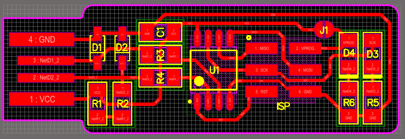
The components must be installed in the correct orientation. I checked that each component is in correct orientation. I followed the instructions carefully.
- The zener diodes are marked, both in the drawing and on the packages, with a line on the cathode side.
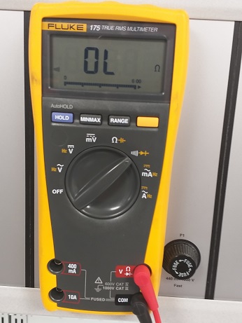
- The LED cathodes on the PCB drawing are marked with dots and thicker lines. Package marking conventions differ between LED manufacturers, but there is usually a green or black line visible on the cathode side of the epoxy lens. Some LEDs have an extra copper marker on their cathode pad on the bottom. Some print a small arrow on the bottom, which corresponds to the schematic symbol: the arrow points towards the cathode. If in doubt, you can use a multimeter in the diode check mode; the LED will glow slightly when the red probe is on the anode and the black probe is on the cathode (this is also useful for determining color).
- The ATtiny45 marks pin 1 with a dot laser-etched into the corner of the package. Pin 1 is marked in the drawing with a dot as well.
Improving the USB Connector
To ensure a good USB connection, the following improvements were done:
Flow some solder onto the USB contacts on the board to build them up a little bit. Heat the pad and apply solder, moving the iron tip along the pad to distribute it. Once you have enough solder, wipe the iron tip across the pad in one continuous motion to even it out into a smooth layer.
I added a little more thickness to board by gluing some extra material to the bottom of the PCB, I used a thin piece of plywood.
Checking The Work
It is always good to check your work before plugging in a board. It only takes a couple of minutes and can save you headaches down the road.
- Check your board against the schematic and PCB layout image to make sure that you have installed the correct components in the correct locations and orientations.
- Inspect your board visually. Components should be flat on the board, not tilted with pins in the air. Solder connections should be smooth, and solder should have flowed both onto the pin and onto the pad. If you still see a lot of exposed copper on the pad, or the solder is lumpy and draws up into a point where you removed the iron, you probably don’t have a good connection. Reflow by applying heat and flux (either from a flux pen or by adding a tiny bit more solder). Also look for unwanted solder bridges between nearby traces and pins.
- Use a multimeter to check for shorts between VCC and GND.
All previous steps were done and board seems very good!

Programming the PCB by FabISP programmer
After finishing assembling and testing, I had to set up my development environment. I followed Brian’s instructions for Software Installation for Windows and Using the GNU AVR toolchain on Windows 10.
Installations for setting up the development environment
1) First, install the Atmel AVR Toolchain for Windows and run the installer. Pay attention to extract the files to C:\Program Files.
2) Next, download Gnu Make and launch the installer. Accept the default location for the installation to be C:\Program Files (x86)\GnuWin32.
3) Download avrdude, unzipp the folder and copy the archive ‘avrdude’ inside of it to C:\Program Files.
For finishing these tool installations, modify the Environment Variables /Paths in order to tell Windows the locations of the tools.
As Brian advices, I added following three lines into the list:
C:\Program Files\avr8-gnu-toolchain\bin
C:\Program Files (x86)\GnuWin32\bin
C:\Program Files\avrdude
and confirmed the modifications by clicking OK for each of the windows opened.

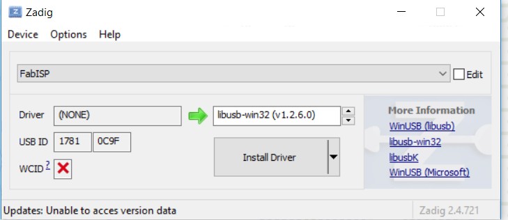
4) Next step and as a last part of the installations, was to install drivers for my programmer. For Windows users, Brian advices us to use a helpful tool Zadig.
I plugged in the already programmed programmer, which I borrowed from our local instructor and selected the “USBtinySPI” device in the list.
Then I installed the driver libusb-win32.

Checking the installation
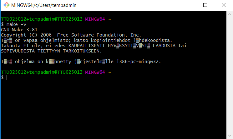
In order to check that everything are in the right folders and installations are finished succesfully, I opened Git Bash and gave command make -v. - > “Command not found”. This indicates that my environment variables are not ok. After careful checking I was not able to understand what was the problem. Finally my local instructor Jari noticed that in my laptop the Git needs to be “run as administrator”. Now it worked!
After that I did following checks:
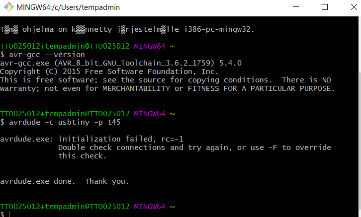
avr-gcc --version and press enter
Connect your programmer to a USB port and type: avrdude -c usbtiny -p t45 and press enter.
Building the Firmware
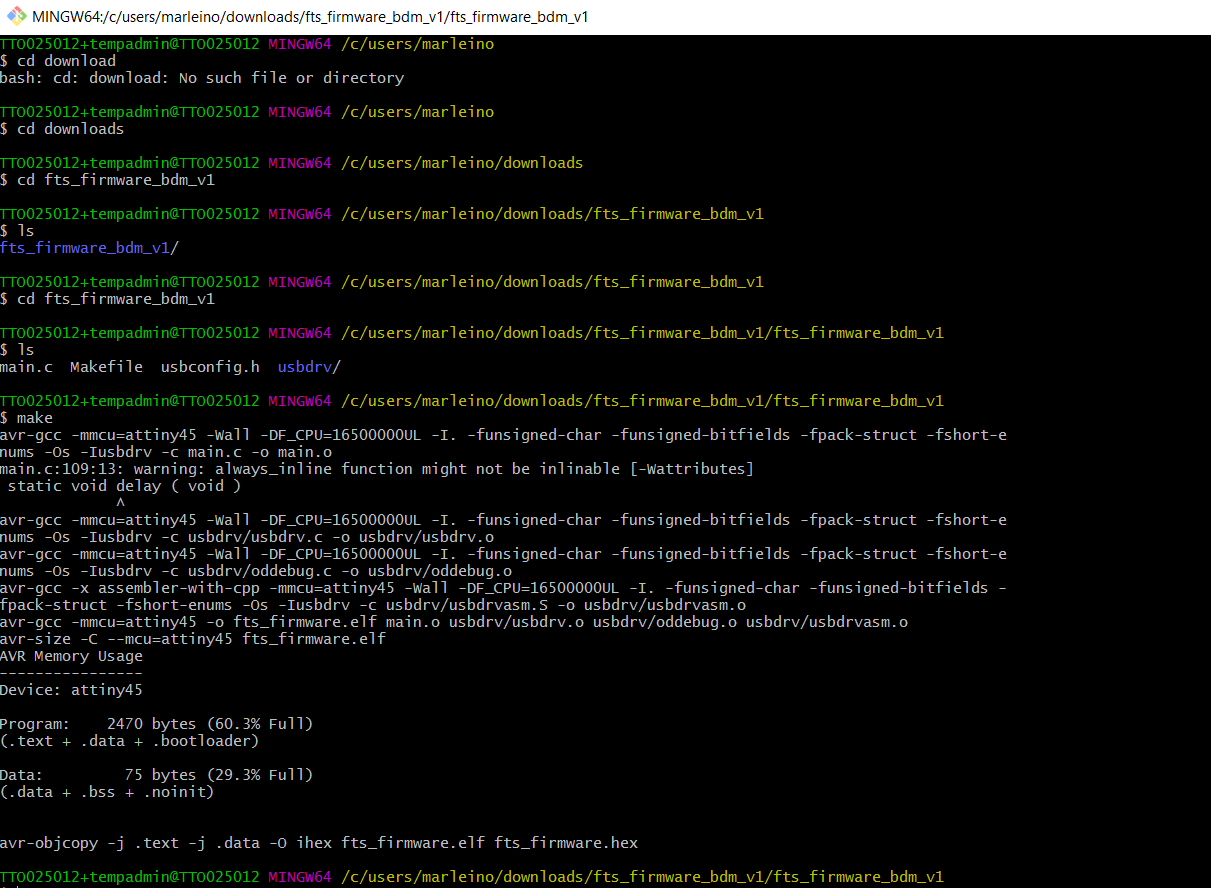
I downloaded the firmware source code fts_firmware_bdm_v1.zip and extracted the zip file. In Git Bash (run as administrator!), I navigated into the source code directory [C:...\fts_firmware_bdm_v1\fts_firmware_bdm_v1], and ran make. The command built the fts_firmware.hex -file, that I am going to program onto my ATtiny45.
Programming the ATtiny45
The Makefile, by default, assumes that you’re going to use a programmer in the usbtiny family.
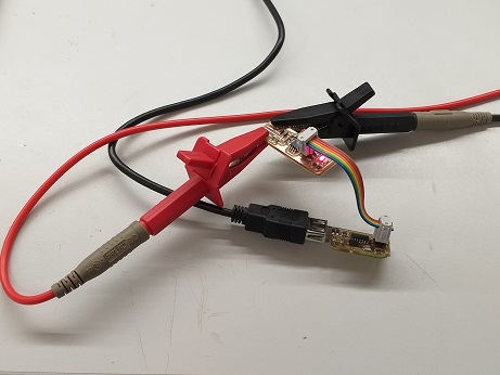
I plugged my board into a USB port by using extension cable, in order to avoid damaging computer’s built-in USB ports by soldering tin.
Next I connected programmer to the ISP header on my board checking carefully the orientation of the cable so, that pin1 (marked with small dot in the board diagram and in the ATtiny45 microcontroller) was connected to pin1.
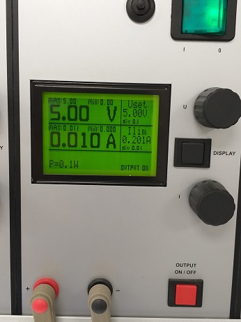
The programmer I used, did not provide power the board to be programmed, so I needed external power or free usb port. I got the red LED light up.
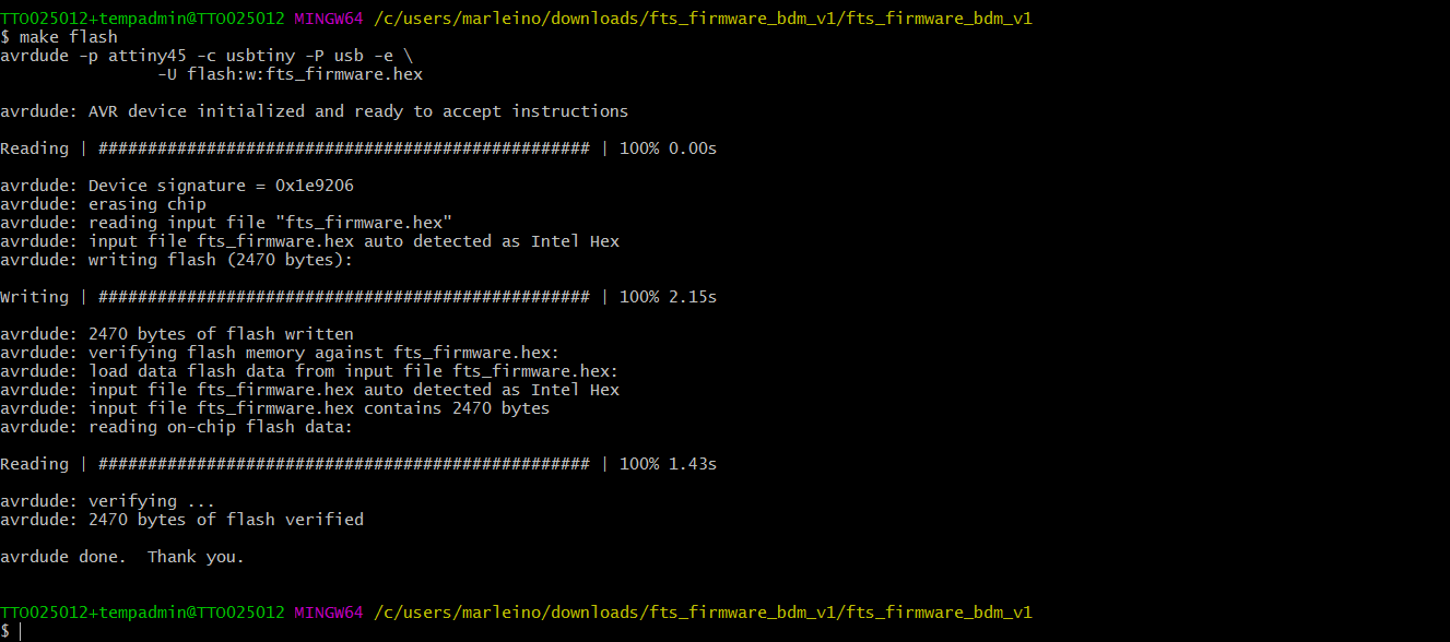
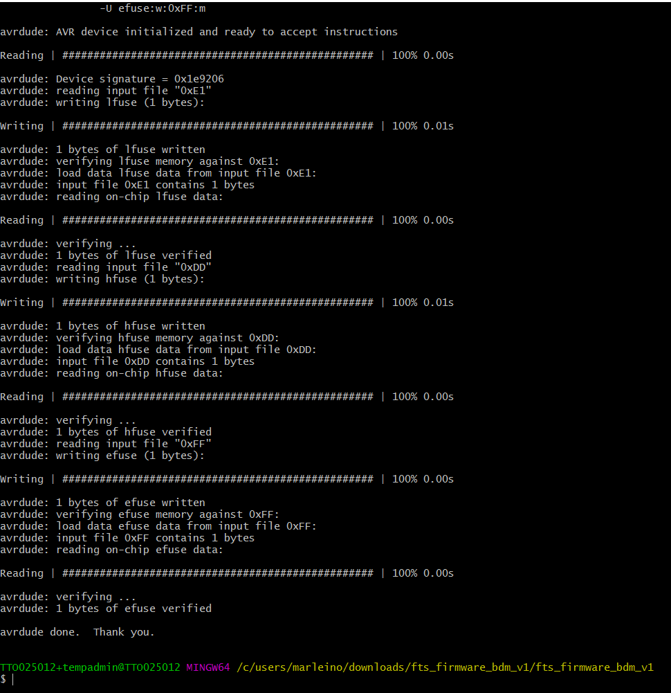
Then I ran make flash. This will erase the target chip, and program its flash memory with the contents of the .hex file I built before.
Next I run make fuses command. This will set up all of the fuses except the one that disables the reset pin.
Test the USB Functionality
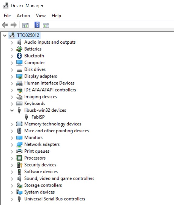
Now we’ll check to make sure that the USB on your board works, before blowing the fuse that will enable it as a programmer. Unplug your board from the USB port and disconnect the programmer, then plug it back in to the USB. Make sure the programmer you used to program your board is also disconnected from the computer.
I opened Windows Device Manager and FabISP can be found!
Blow the Reset Fuse
First, we need to change the bit that will turn the ATtiny45’s reset pin into a GPIO pin. Once again, this will disable our ability to reprogram this ATtiny45 in the future, which is why we wanted to make sure everything was working before doing this.
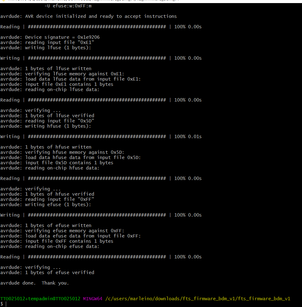
I connected the ISP programmer to the board one more time, and run make rstdisbl. This does the same thing as the make fuses command, but this time it’s going to include that reset disable bit as well. You should see some progress bars, and with that, avrdude will never be able to talk to this chip again through the ISP header.
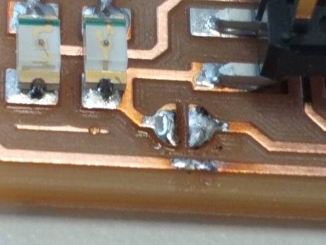
Second, VCC needs to be disconnected from the Vprog pin on the ISP header by removing the bridge on the solder jumper. I used desoldering braid to remove the solder from the jumper, thus breaking the connection.
Problems
Environmental Variables were not correctly modified. I needed to read instructions again and re-do this part. I needed to separate the values by semicolons.
I had problems in running make -v. I repeatedly got message “Command not found” and I thought I still have problems with the environmental variables path. Finally Jari (local instructor) noticed that I need to run Git Bash “as administrator” to get this working. This was required also later with Git Bash commands.
The programmer that I used was not giving power to my board and my laptop has only one USB port. I needed to use external power source.
Files
Linetest traces
Linetest outline
PCB traces
PCB outline
Firmware hex file