7. Electronics design
Group assignment
Use the test equipment in your lab to observe the operation of a microcontroller circuit board
Individual assignment
Redraw the echo hello-world board, add (at least) a button and LED (with current-limiting resistor), check the design rules, make it, test it.
Individual assignment
Board design
I used Autodesk Eagle for the design.
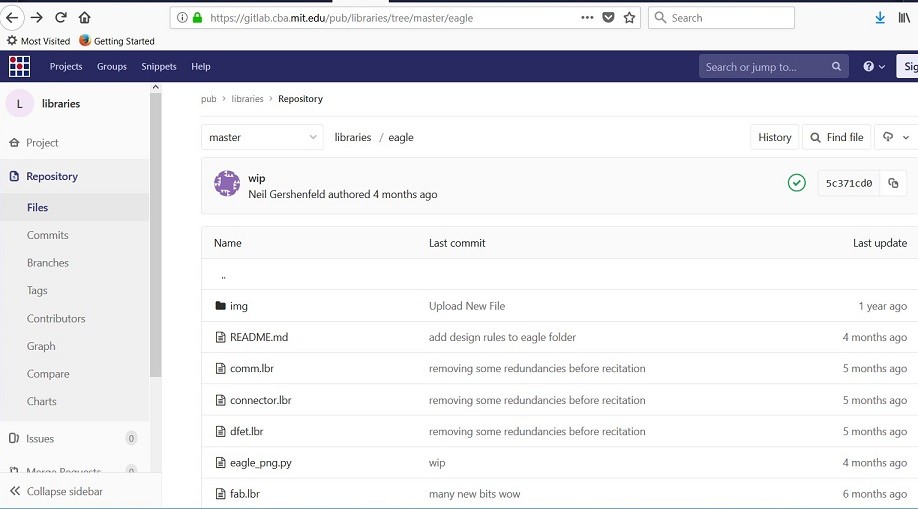
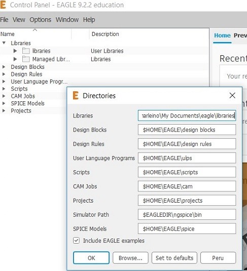
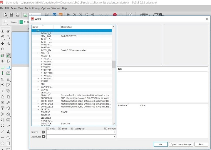
First I uploaded Eagle libraries from Gitlab to Eagle and defined the library path to Eagle Directory. Fab-library (file fab.lbr) contains the components typically used in Fab Lab.
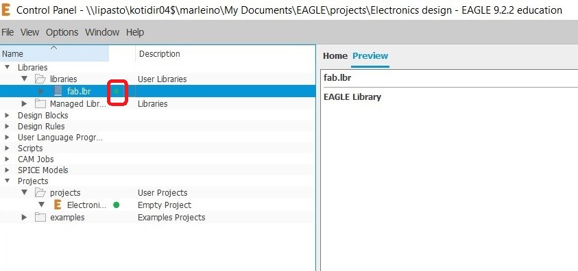
Then I activated the fab library by pushing the dot -> it will turn green when active.
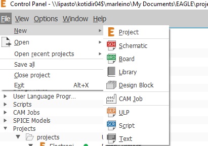
I created a new project and named it Electronics design and created a new schematic.
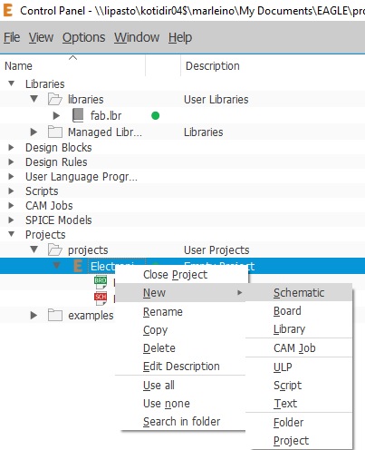
I was ready start adding components from the libraries. The needed components I checked from the Hello-world board picture.
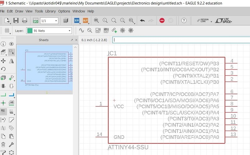

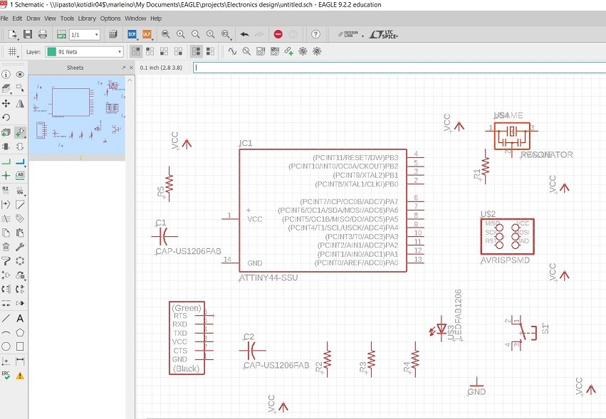
After having all components, the components can be connected. This is done with the operation “Net”.
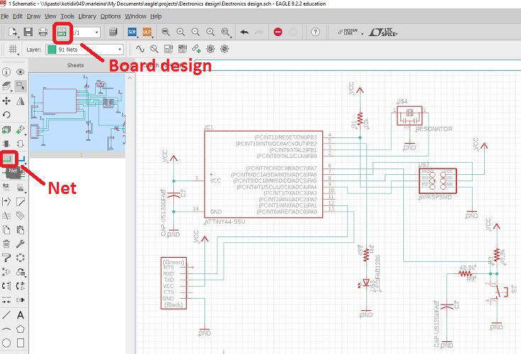
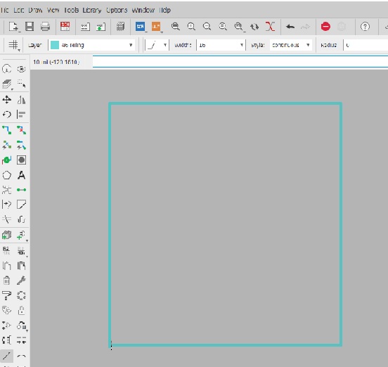
When the schematic is ready, you can start the board design (see previous picture).
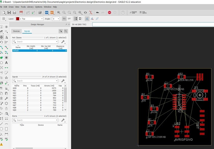
Components will be moved so that the positions are optimal for the connections. The components should be moved and rotated on the board in a way that their connections are short and in a logical order. Press ratsnest button in the side panel time to time to calculate the shortest wires between connections. When positions are optimal, components are connected with “Route” tool. Set the DRC settings to 16 mil for all the options.
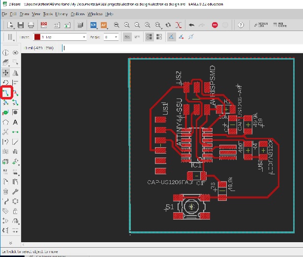
Next create an line around the board with “Polygon” tool, name it GND and press ratsnest to create GND everywhere in the board, where it is not restricted by your connections.
Press ERC (Electrical rule check) and DRC (Design rule check) to see if there are any unwired connections or other problems. They show where the errors are in board.
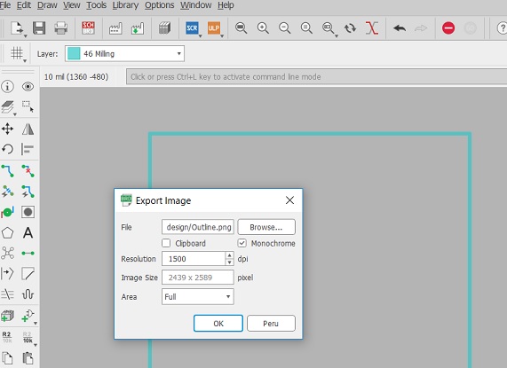
Now you can create line around the board in the milling layer to create outline for the milling machine.
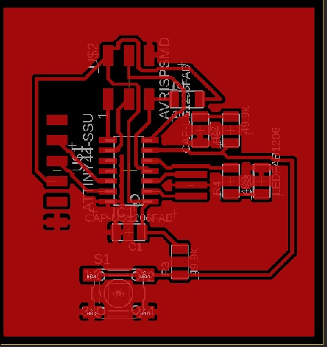
Change the background color to white Options -> User interface Layout -> Background -> White. Then select only milling layer and File -> Export -> Image. Select the location of the file, set the resolution to 2400 dpi, select monochrome box and ok.
Change the background back to black, select top layer and export the trace file for the milling machine.
Now the png-files are ready for the milling machine and mods tool.
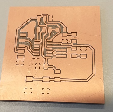
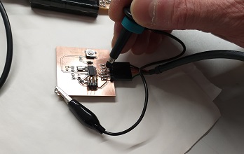
Board milling and assembling
Milling was done according to week05 Electronics Production assignment.
Here are the needed components
- 1x ATtiny44A microcontroller
- 1x 2x3 Pin header
- 1x 1x6 Pin header
- 1x 1 uF Capacitor (C2)
- 1x 10 nF Capacitor (C1)
- 1x 20 MHz Resonator
- 1x 499 Ω Resistor (R4)
- 1x 10 kΩ Resistor (R1)ok
- 2x 49,9 kΩ Resistors (R3, R9)ok
- 1x 6mm Button
- 1x red LED
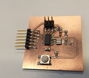
And after soldering here is the board
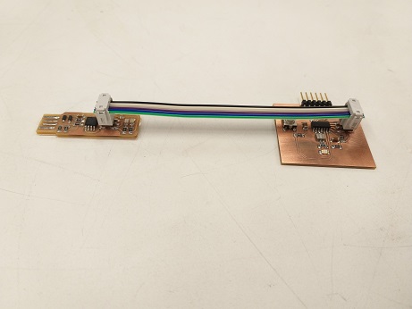
Cable for programmer
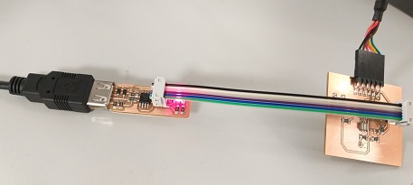
I made a cable for the programmer, for that I needed 2 x SPI header and 6-way ribbon cable. I used vice to close the headers.
Programming the board
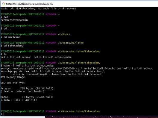
I downloaded the hello.ftdi.44.echo.c.make and hello.ftdi.44.echo.c files for the programming and testing of the board.
First I compiled the codes with make -f hello.ftdi.44.echo.c.make.
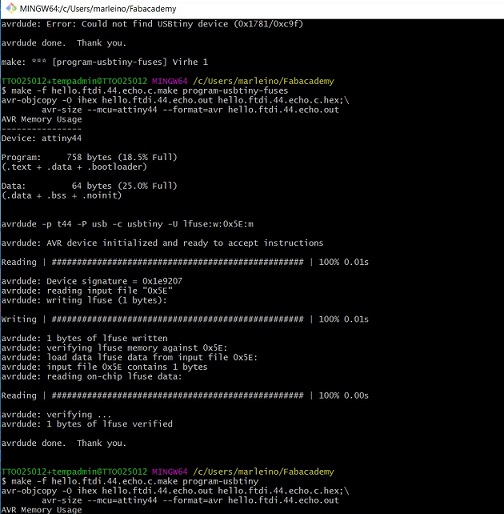
Next I set up the microcontroller for programming with make -f hello.ftdi.44.echo.c.make program-ubtiny-fuses.
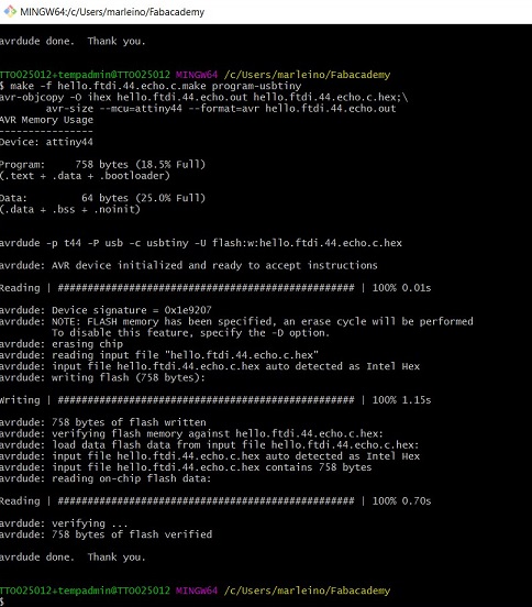
Then I flashed the program to microcontroller’s memory with make -f hello.ftdi.44.echo.c.make program-usbtiny.
Problems:
First the programming failed. I got error message “Could not find USBtiny device”.
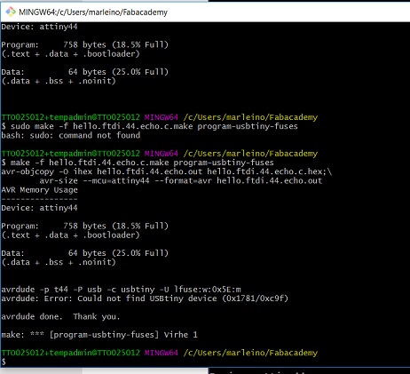
I had no power coming to my board, so I needed to attach FDI cable to the board. Now I can see the led light on, that indicates there is power for the board.
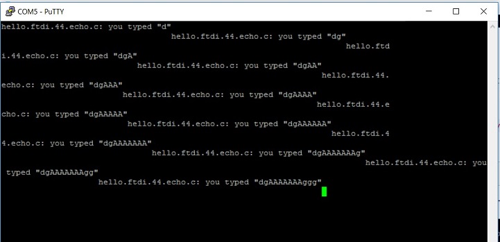
Testing the board
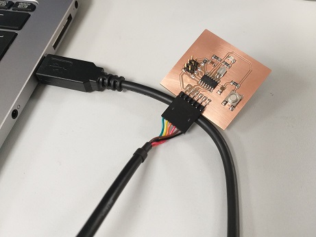
I removed the programmer and connected the programmed board to my laptop with FTDI -cable.
To test the board I opened Putty. I modified the configuration “Connection type -> Serial”, “Serial line -> COM5” and “Speed -> 115200 (baud rate)”.
Then I pressed “Open”.
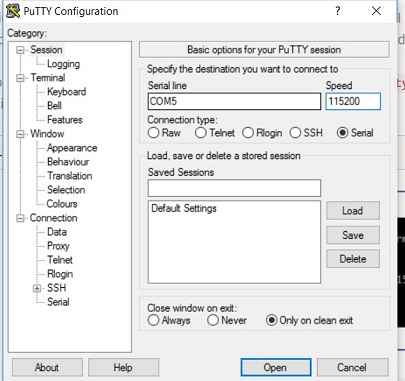
I can now see in Putty terminal everything I am typing in keyboard.
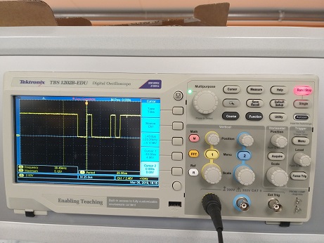
Group assignment
I did the group work with Perttu, Gleb, Lucasz and Michael.
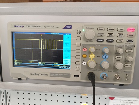
We used oscilloscope to check the signal by connecting the probe.
Baud rate seen in the oscilloscope (11,49 kHz) is near to the Speed defined in Putty configuration (115200).
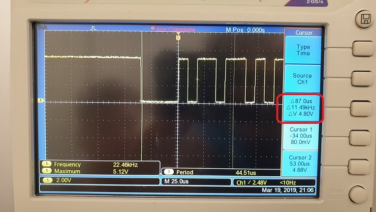
Typing a letter using keyboard, you can see the binary format of the letter in oscilloscope.
Using Putty, we typed U, S and B.
Binary code for “U” 01010101. This can be seen also in the signal, you need to look at it reversed, least significant bit (LSB) is sent first.
Binary code for “S” 01010011.
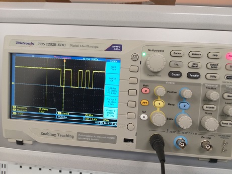
Binary code for “B” 01000010.
Files
Eagle schematic file
Eagle board file
Trace png
Trace rml
Outline png
Outline rml