14. Networking and communications
In this, week I designed and milled a board for the networking assignment. The board was for IR sensors wthat are to be used as input devices for my final project. Our instructor for the week was Juha Mäkelä who gave tips on how to complete the assignment.
Assignment
Individual task
Design, build, and connect wired or wireless node(s) with network or bus addresses.
Group task
Send a message between two projects.
Group Assignment
We did the group work together. We downloaded the Bluetooth Control Lamp app from Google’s Play Store and set it up as presented in the image below.
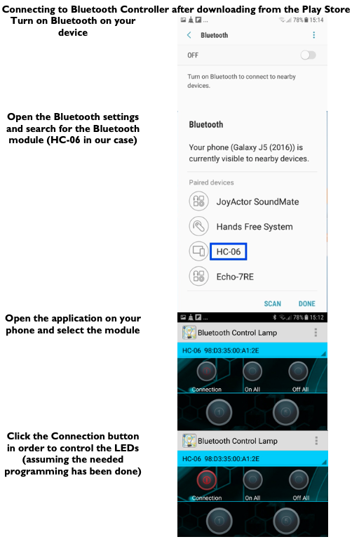
After the module is paired and the code for serial communication compiled and uploaded to the microcontroller, the desired functionality can be obtained. These includes commands to blink LEDs on the press of a number as outlined below.
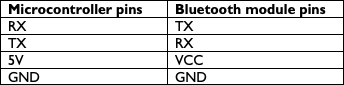
We connected Sahan’s, Yasir’s, Jobin’s and my board from a previous assignment. Using HC-06, a Bluetooth slave module for wireless serial communication, we connected and programmed our boards from Electronics design week to blink the LEDs when a button on the Bluetooth mobile application is pressed. GND and VCC were provided from one board and all the boards were connected using a flat ribbon cable (FRC). The module works with serial communication and can be configured to send commands when connected to a mobile phone or any other Bluetooth device.
The LED on each board lit up when the button corresponding to the number assigned to the node was pressed. Finally, the code was modified so that all the LEDs turned on and off at the same time. The module enables the Arduino to easily connect and exchange data with devices such as Smartphones, computers or other microcontrollers.
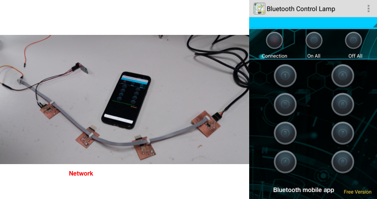
Below is a video of the connected boards.
More details about the group assignment can be found in Jobin’s and Sahan’s pages.
Individual assignment
I had started working on the final project board in output devices week, which I hoped to use for the following related tasks. The board (still in progress) took longer to route than anticipated and after spending much time working on it, could not afford to spend more. So, for this week’s assignment decided to design one based on IR sensors that I intend to use for the final project. The design process followed that in Electronics production and design weeks.
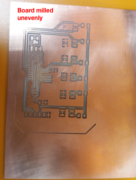
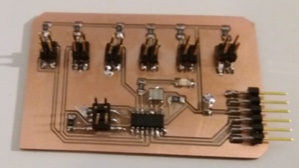
Even though I had used similar settings for all the previous boards, they did not work with the current board. The first time I tried to mill, the board was not evenly placed on the surface of the milling machine. There were deeper cuts in some places on the board ruining some traces and it was not worth repeating the job. The second time, the board was well placed but the milling bit was going deeper than expected which removed some of the traces.
Finally, with Behnaz’s suggestion, we decided to reduce the cut depth from 0.1mm to 0.08 mm in fab modules and this worked.
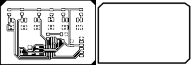
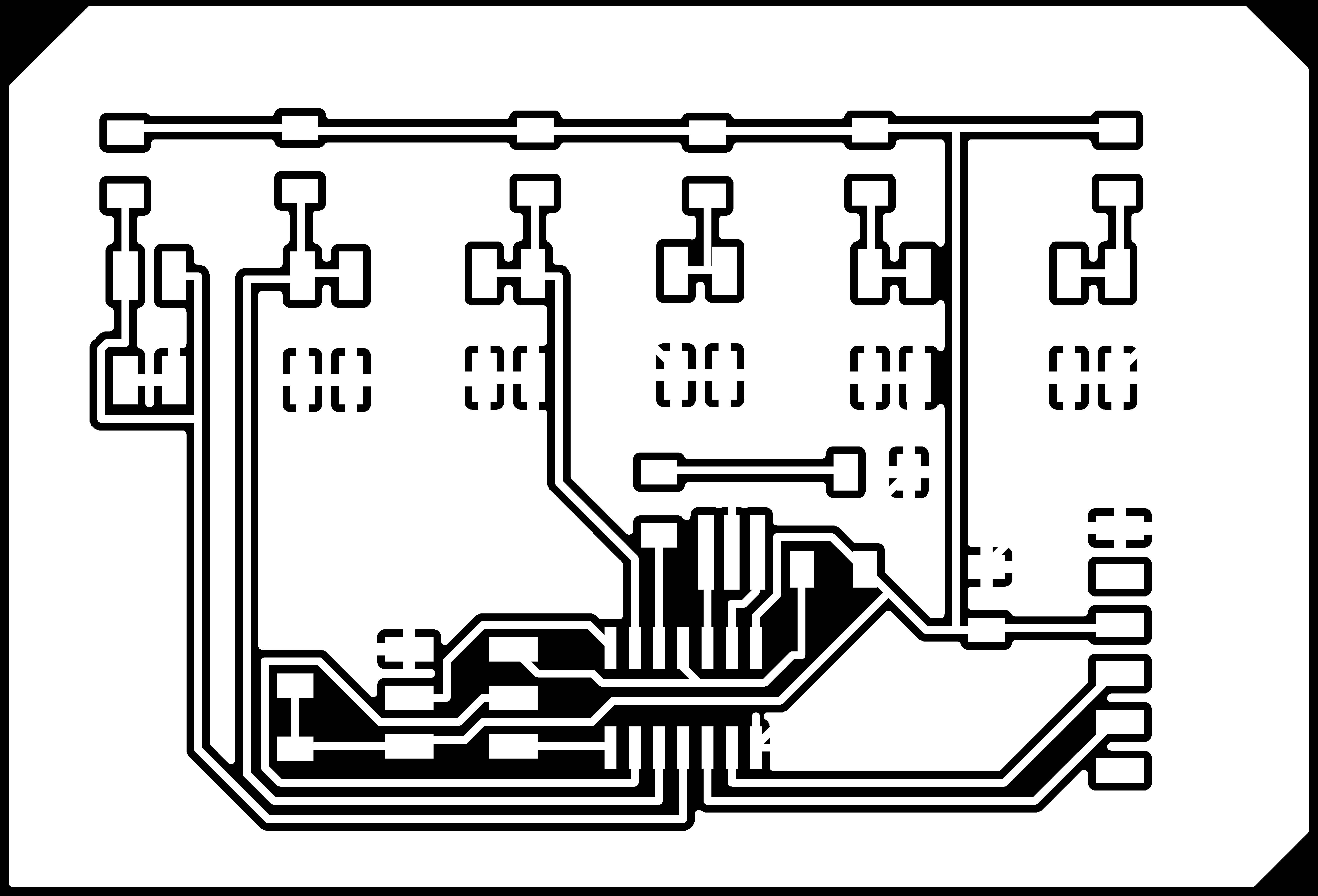
Below are images of the schematic and board design.
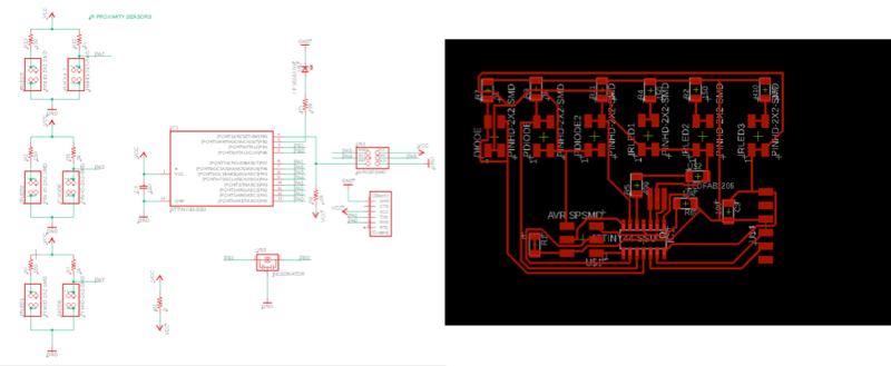
For the traces and outline.
If there is something I haven’t gotten used to yet, it is soldering which took a long time! After it was done, I confirmed that the all the connections were as they should be with a multimeter and everything was working.
When I was leaving the lab I accidentally placed the board in a constrained space which pressed against the ISP header pin and part of it came off (lucky me!). Luckily, there were still people in the lab and I went back and re-soldered the header. Again, I checked for continuity with a multimeter and all was ok (sign of relief). When I later tried to program the board, this happened:
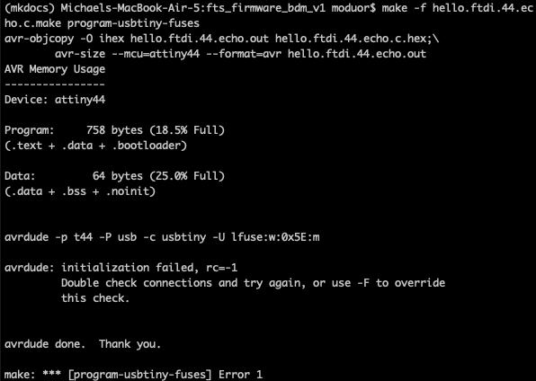
As I was home, there wasn’t much I could do other than try to re-examine the board taking a closer look at all the traces. Underneath the ISP header, not all the pins seemed to be connected to the corresponding IC pins. When removing the connector from the ISP header, disaster struck!
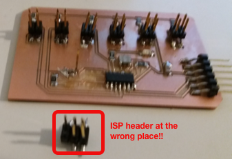
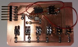
Most of Friday afternoon’s work ruined! Later, Alok helped to reattach the ISP header to the board and using jumper wires, reconnected the broken connections. Although, it needs to be treated gently when attaching the connector for programming as it has poor stability and could easily detach from the board again when removing the connector.
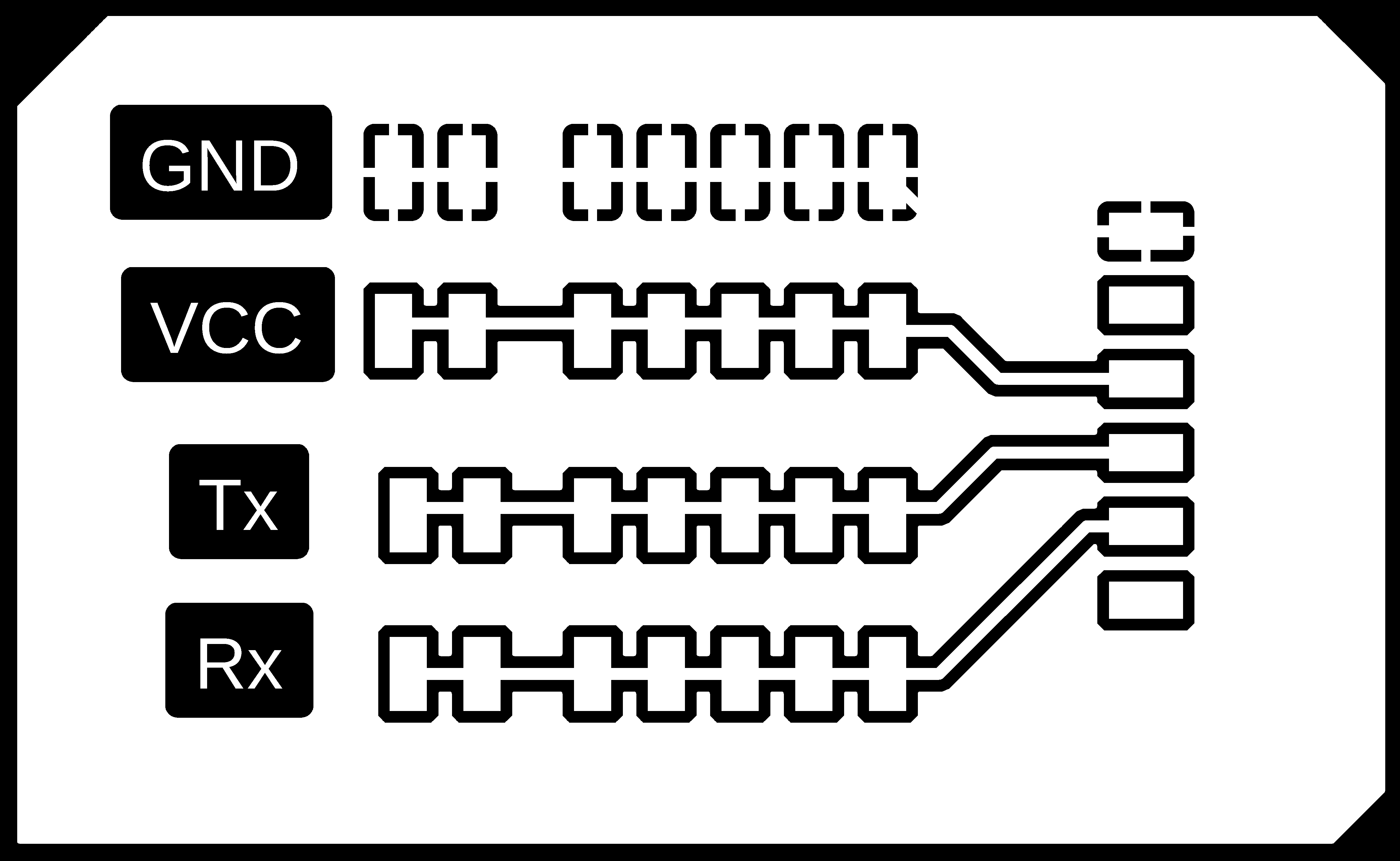
After this, following Jari’s example from 2018, I made an rx/tx hub connector. With this board, there were no problems with milling. I also used the code and followed the description by Jari to connect my boards as serial bus.
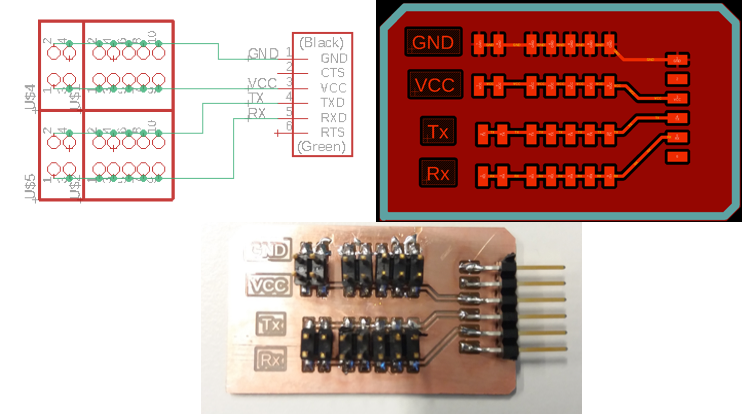
The key idea is that when the node sends a response, the Tx pin is switched to output state and back to input after sending. The default state is input to not interfere with other nodes.
Using this connector, I built a network consisting of the boards from Electronics design (Node 1), Input devices (Node 2), this week (Node 3) and programmed them. As I was only blinking the LEDs, the pin configurations were similar to those used in Embedded programming week. The LEDs in all three boards were attached to PB2 (Pin 5) which corresponds to Pin 8 on the Arduino.
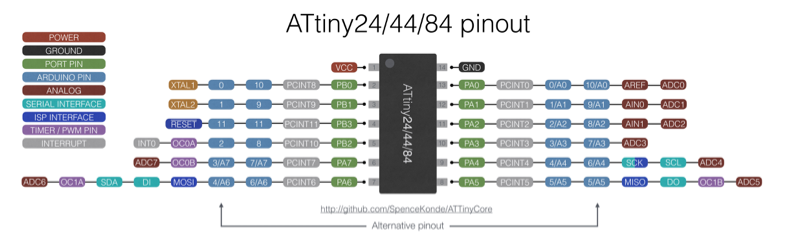 ATtiny44 and Arduino Pinout
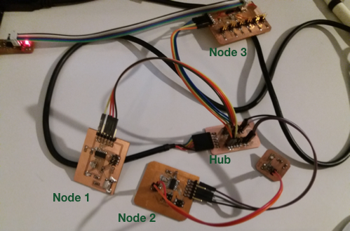
Wired node
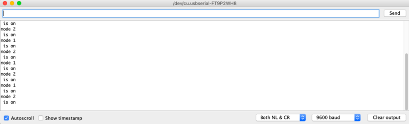
When I type a node number (either 1, 2 or 3), in Arduino IDE’s serial monitor, the LED on the board blinks and the node number is printed. Nodes 1 and 2 work as expected but there is no response or any output given from the third node. I will revisit this later when I have time.
Files
- Arduino -
- Group work - Group zip file
- Individual - Node 1 / Node 2
- Eagle design files
- IR sensors Schematic 1 / Schematic 2 / Board 1 - this is a modified version of the first one which is not routed / Board 2
- Hub - Schematic / Board
- PNG
- RML
NB: I did not create RML files for the second board which is mostly similar to the other one, except for the placement of a few components. I had a resistor close to the resonator in the first one and only noticed after preparing the RML files so decided to modify the schematic by leaving some space in case it would be a problem.