ASSIGNMENTS
Group
- Characterize the design rules for your PCB production process.
Individual
- Make an in-circuit programmer by milling the PCB and program it.
TOOLS and SOFTWARE
Fab Modules
Roland Milling Machine
Soldering Tools
The main purpose of this week was to introduce us to the basics of electronics and for us to understand how the process of producing an electronic board and programming it.
My background is Electrical engineering, so I'm familiar with the concepts of electronics and PCB. However, during my years of study, we always use commercial programmers for our projects. That's why, I was excited to learn how to fabricate my own programmer which then I can use to program other boards.
Fab TinyISP
The Fab TinyISP is an AVR ISP (In-system programmer) board designed to be produced in a Fablab and then it allows the user to program other boards.
During the global session, Dr.Neil discussed the different designs provided and I decided to go for Brian since it was the one used in the Fab academy tutorial and the documentation was good with me.
The Fabrication Process
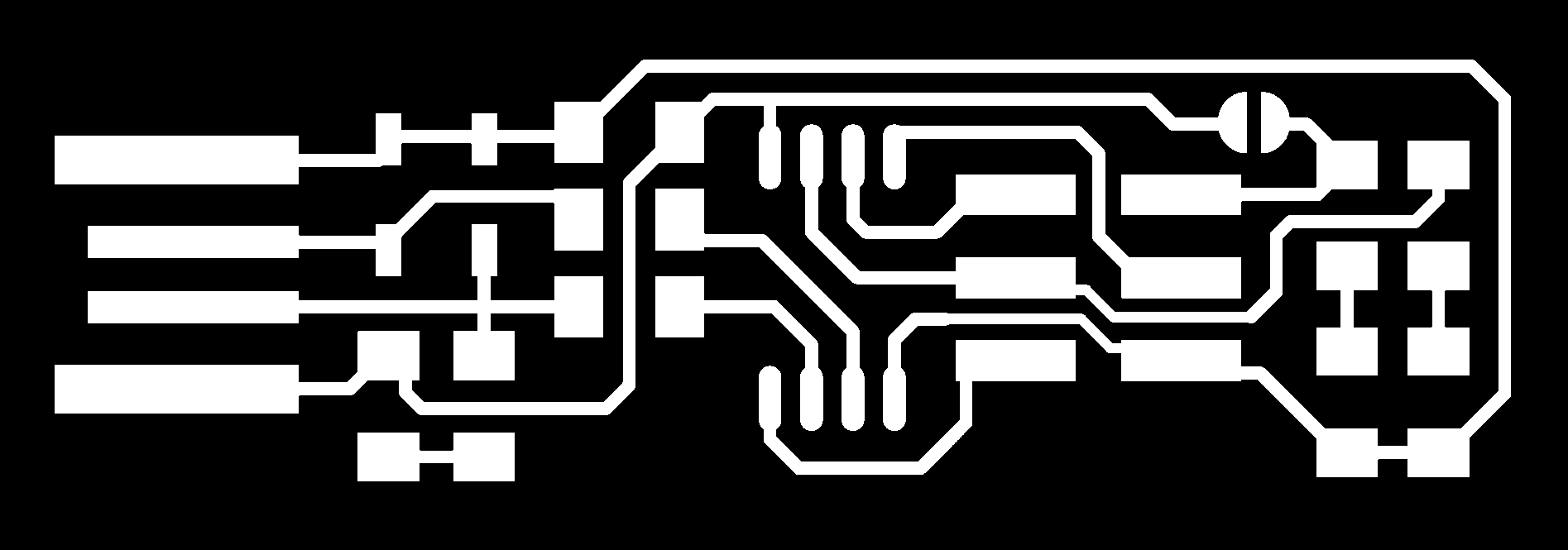
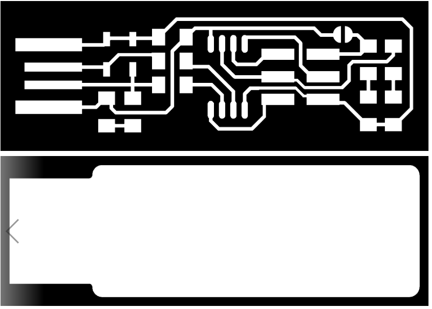
1- I downloaded the provided design's Traces and Outline cutout png files.
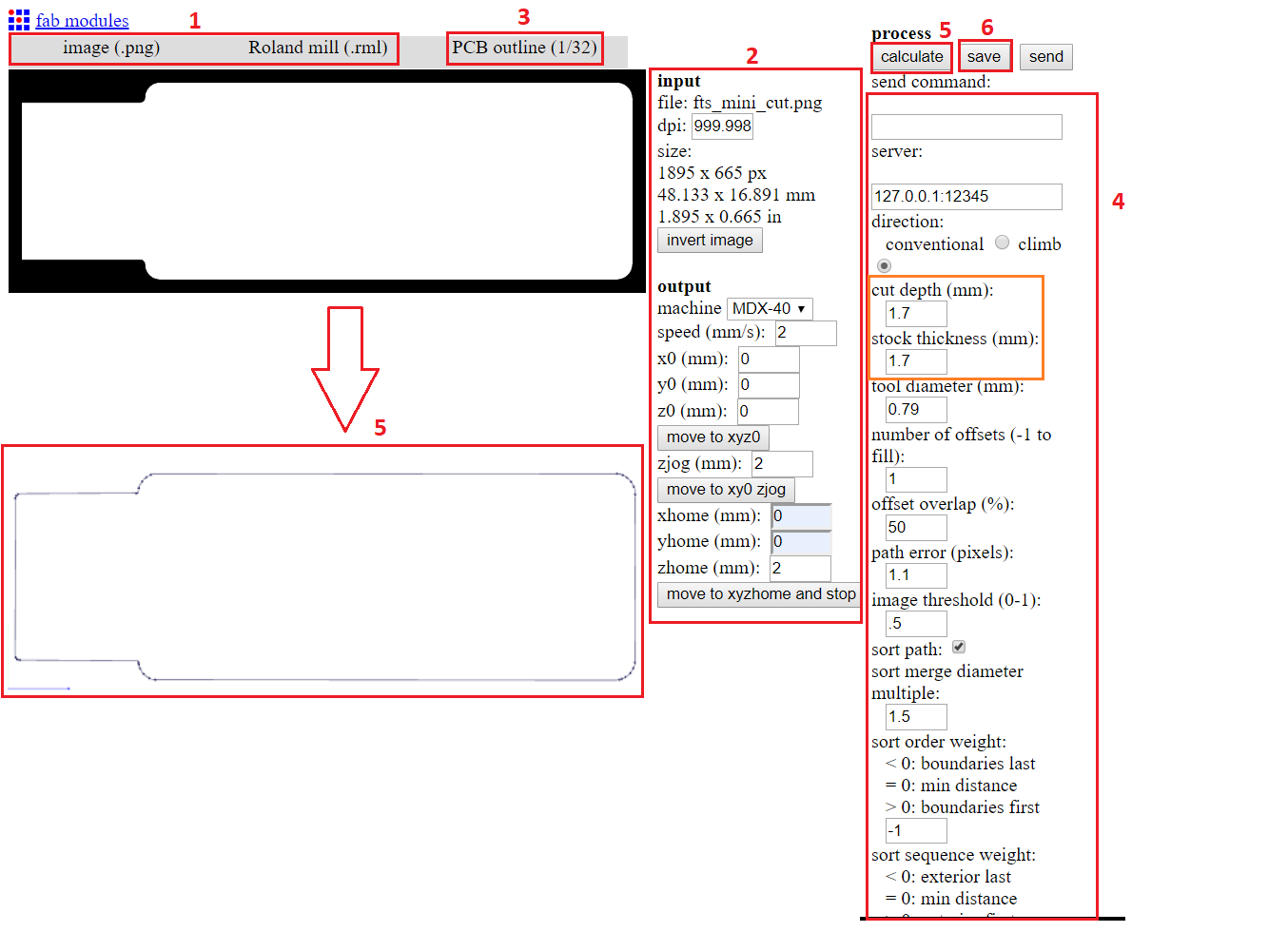
2- I went to Fabmodules.org to prepare my files to be fabricated using the Roland MDX-50 milling machine availabe at our Fablab. I started with the traces file first and I went to input format > image(.png) > selected the traces .png file > output format > Roland mill (.rml)
The output settings appeared on the right side of the screen. Here I added the details and parameters suitable for my machine after I consulted with one of the instructors. The output settings I entered are shown in the image below.
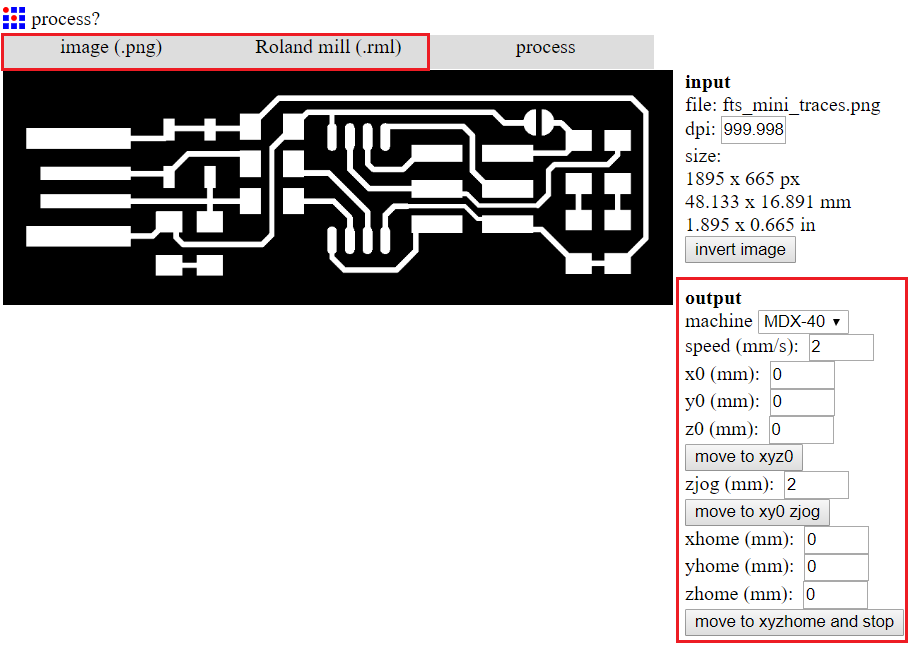
Once I entered the output settings values, the process tab appeared on the top toolbar and I went to Process > PCB traces (1/64). Now, the data for the milling process were automatically generated and I clicked 'Calculate' to generate the RML file. The traces and milling paths will now be created and then I clicked on 'Save' to download the RML file to my computer.
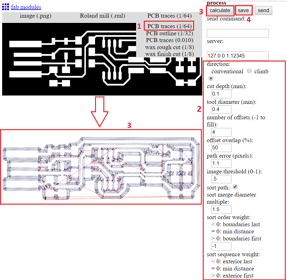
3- I repeated the same steps to generate the RML file for outline file. However, there were some few modifications that I did in the cutting tool and the output settings. These changes are as follows:
- - In the 'process' tab, I selected 'PCB Outline (1/32)'
- - In the settings that appear after selecting the process, I changes the value of the stock thickness based on the thickness of the board I will mill. Also, I changed the cut depth (the depth the tool will cut in one pass) to a value equal to my the thickness of my material becausre I wanted the machine to cut it in one go.
The Milling Process
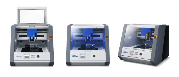
As I mentioned previously, I used the Roland Modela MDX-50 machine to mill my PCB board.
4- I placed the copper board I used for milling on top of the sacrifice wax block and made sure it's properly fixed using double-sided tape to stick my copper board on the wax bloack.

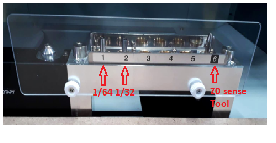
5- I needed to set up the machine for milling. I started by fixing my tools in the tool holder and then placed them in automatic tool changer slots (1/64 for milling and 1/32 for cutting).
6- Next, the Z-level must be probed everytime the board is moved or replaced. I followed these steps to probe the Z-level.
- a- I used the Z-probe that comes with the machine and snaped it to its place and placed the small golden metalic part on top of my board and closed the machine's door.
- b- From the machine's control panel, I pressed on 'Menu' button multiple times until it displayed the "ATC Tool" menu which is used to change the tools. Using the hand wheel, I selected the tool used for Z probing (Shown in the image below) which in my case was placed in slot 6 so I chose'TOOL 6'. Now , the machine's head will move to the specified slot to the pick the tool I selected.
- c- Once the machine finished picking up the tool, I kept pressing the 'Menu' button multiple times until I reached the 'User' menu beacue I wanted to move the machine's head and align it so that it's facing the top of the z-probe's gold part. To do that, I pressed on the green 'X' button to move the machine in the x-direction and I used the hand wheel to move it where I want and then I pressed the 'Y' button and moved using the hand wheel until the head was facing the probe.
- d- I pressed on the 'Z0 sense' button to start the procedure and a message appeared on the screen asking me to confirm so I pressed the 'Enter' button. The machine started going down slowly until it touched the Z-probe. Once this process was done, I opedned the door and removed the z-probe.
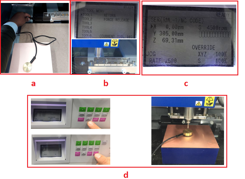
7- Before starting the milling, an origin point should be set to define where the user wants to do the milling. From the machines control panel, I went to the 'User' menu followed the same steps mentioned previously (Step 6-c) to move the machine in the x-direction I want and then pressed 'Origin' button and kept it pressed until the X-position in the screen became zero and I followed the same steps for the Y position.
8- Last step before milling was to set the spindle speed. To do so, I pressed the 'Spindle' button form the control panel and then used the hand wheel to increase the speed until 5500 rpm as recommended by our instructor.
9- Now, I followed the same procedure in Step 6-b to change the tool to the 1/64 milling tool.
The machine set up is now completed.
10- I opened the V-Panel software and selected 'Cut' icon to start milling and a window to upload the files appeared so I clicked on 'Add' and uploaded the traces file. Finally, I clicked on 'Output' and the machine started milling the traces.
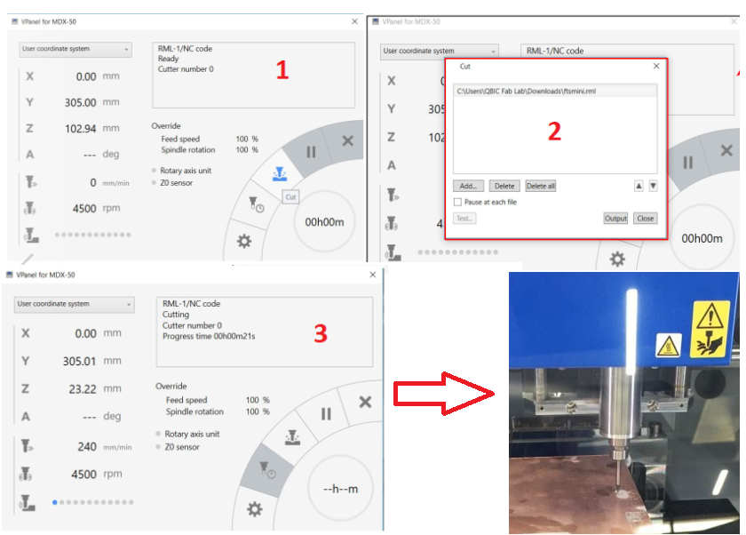
11- Once the traces milling was done, I followed the same steps in Step 6-b to chnage the tool to the 1/32 cutting tool.

12- I followed the same steps as in Step 10 to upload the outline file and the machine cut the outline sucessfully
Here's the Fab TinyISP after the milling process

Soldering Components
Imagine you're making a poster and you have some pieces you need to put on that poster, how would you do that ?... You're most defenitely going to use glue to stick those pieces on the poster. That's basically soldering!, the poster here is your milled board, the pieces are the electronic components and the glue is the solder (A type of metal with a low melting point).
For this board I used SMD (Surface-mount device) components which are a type of electronic commponents produced using the surface-mount technology which means they're manufactured to be directly placed on the surface of a PCB through the different techniques of soldering.
I'm quite familir with soldering, but I haven't soldered SMD components before so it was interesting to apply the techniques I learned into something new.
13- First I collected all the required components which were available at the Fablab inventory. These are the components I collected (Also shown in the image below):
14- I prepared my soldering station with everything I need and turned on the soldering station and the smoke absorbing fan as shown in the image below.
15- I used the schematic and board images from the Fab academy tutorial page(Shown in the images below) as a refernce for the components placement.
16- The technique I used to solder the components is very simple. I did the following steps to solder each component:
- a- I put flux on the components pads which enables the solder to adhere to the metal surface instead of going all over the place.
- b- Then, as recommended by Dr.Neil, I placed some solder on one side of the copper pad by melting the solder wire using the soldering iron.
- c- using tweezers, I picked the component and held it down in its appropriate place.
- d- While holding down the component with one hand, I used my other hand with the soldering iron and heated the area where I placed the solder previously in (b) until it melted around the joit and I removed the iron. Once the solder cooled, one side of the component was fixed and soldered.
- e- Now that one side is soldered, I didn't need the tweezers. To solder the other joint of the component, I simply used the iron to melt a small amount of solder to fix the joint.
I followed the same steps listed above to solder all the components. In addition, when soldering the components, I tried to be a bit fast and not place the iron at one component for too long to avoid overheating the component and damaging it.
17- Once I was done soldering all the components. I added some solder and made sure its smooth onto to the part that will go inside a USB port to build it up and improve the USB connection later on.
One challenge I faced during soldering is that the SMD components are extremely tiny and need practice to learn how to work with them. However, following the soldering tip Dr.Neil mentioned during the class has helped a lot in soldering those tiny buddies :D
Here's the Fab TinyISP board after the fabrication process
Testing and Troubleshooting
18- To test my Fab TinyISP board, I simply connected it to one of the USB ports in my computer and the results were:
This time I connected the board to the USB port and FINALLY the LED turned ON!!
FabISP
Similar to the Fab TinyISP, the FabISP is an in-system programmer designed to be fabricated in a fablab. In this part, I fabricated Dr.Neil's FabISP which uses the ATTiny44 microcontroller.
The Fabrication Process
The fabrication process I followed for the FabISP is the same as the Fab TinyISP (Steps 1-18). Therefore, I'll keep the steps here very short and simple.
1- I downloaded the provided Traces and Outline cutout png files.
2- I went to Fabmodules.org to prepare my files to be fabricated using the Roland MDX-50 milling machine
The Milling Process
3- I placed my copper board in the milling machine.
4- I calibrated and set up the machine.
5- I started milling the board and as mentioned previousy, I used tool 1/64 for milling the traces and 1/32 for cutting the outline. However, I didn't get the milling right from the first time.
Soldering Components
6- I collected the required components. The required components for this board were:

7- I started placing and soldering the components using the labeled board diagram as a reference (Shown below). One tip I followed based on the tutorial is to start soldering the USB connector first because its the most challenging part and then I soldered the second most challenging part which the ATTiny-44 microcontroller.
Here's the FabISP board after the fabrication process

Testing and Troubleshooting
8- Before doing the testing, I used the multimeter to check that there are no short circuits on the board.
9- This board has no LEDs to indicate if its working or not so I tested it using what's called "The Smoke Test". I connected the board to the computer using a mini usb cable and luckily I didn't get any error messgaes related to power surges or that the board is drawing to much power. Therefore, this means that my board has no short circuits and is working fine. Yay!