Week 6: Electronics Design
Assignment
In this assignment we are instructed to choose a software to work with in designing a circuit board and demostrate the workflow. The circuit we have to design is a echo hello-world circuit and add an LED and a button.
I used KiCad software because it was easy to get help from colleagues in our Fablab.
In designing the board I started with a schematic of the circuit.
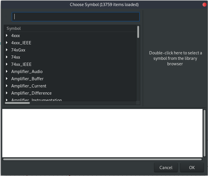
First I import the component I will use to design, and this is the window I import component from.
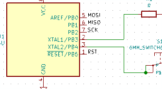
After importing all component needed I connect them using either a label or a wire.
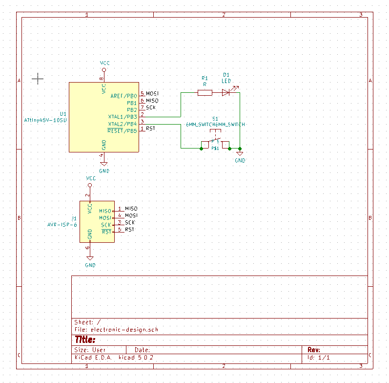
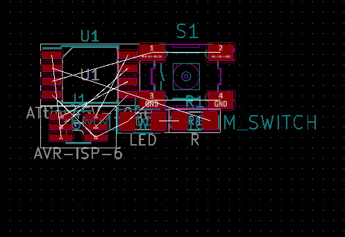
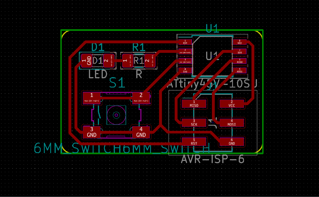
I continue to connect all components, the below image is for the final schematic.
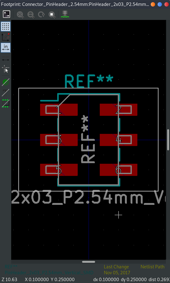
The following step after designing the schematic is to assign PCB footprints to schematic symbols
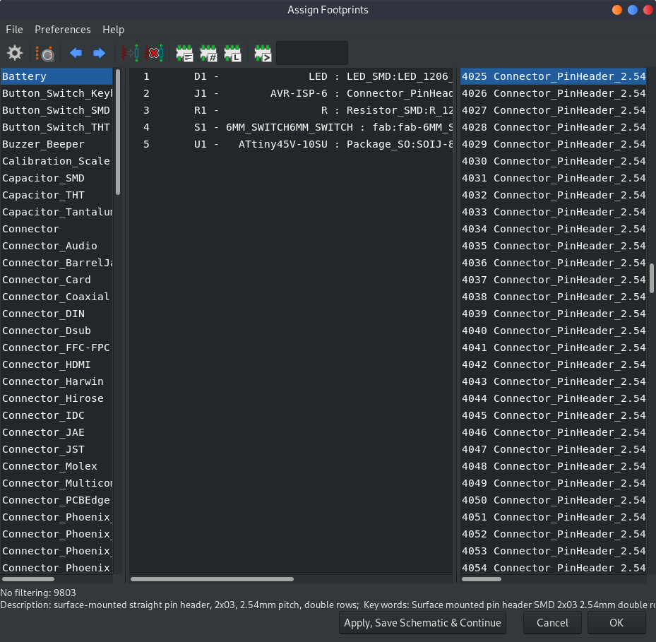
When assigning footprints to the schematic symbols you have a window which shows you the footprint you about to assign and its 3D view so that you can select the perfect component footprint.
Then I continued to design the board of the circuit. I imported the components footprint that I assigned.
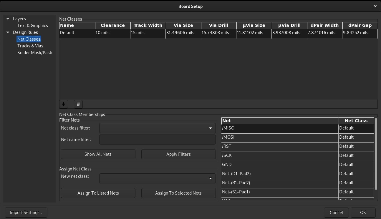
Below is a screen shoot of the design rules I used designing the board.
I aligned all the component before I start joining components by traces.
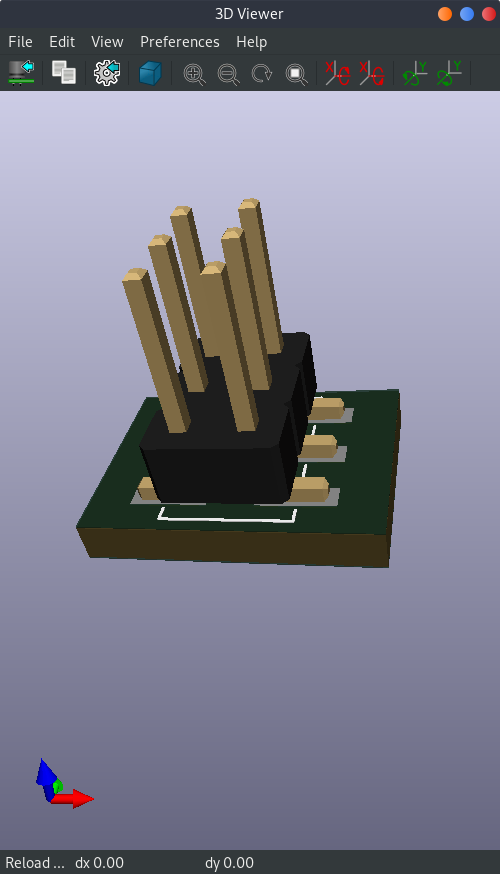
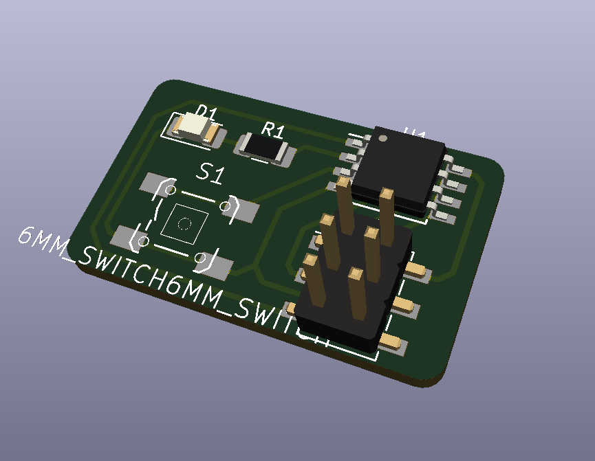
This is the final look of the board in 3D.
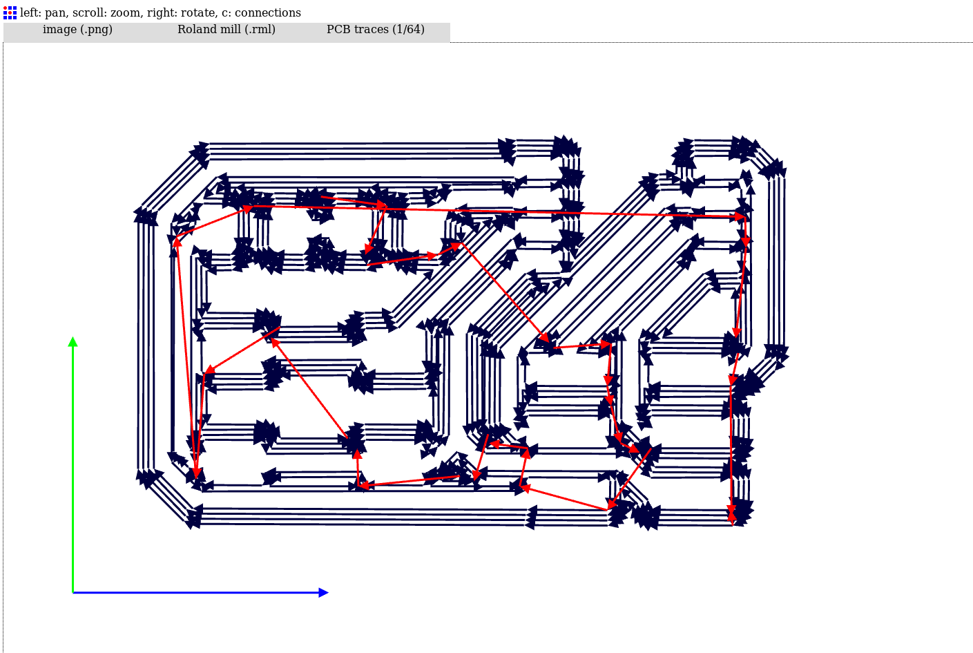
After designing the board I moved on to generate RML file which will be used to mill the board traces.
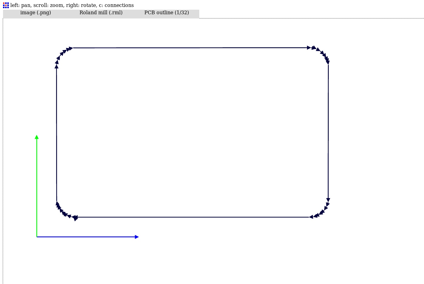
Generated RML file for outline of the board.
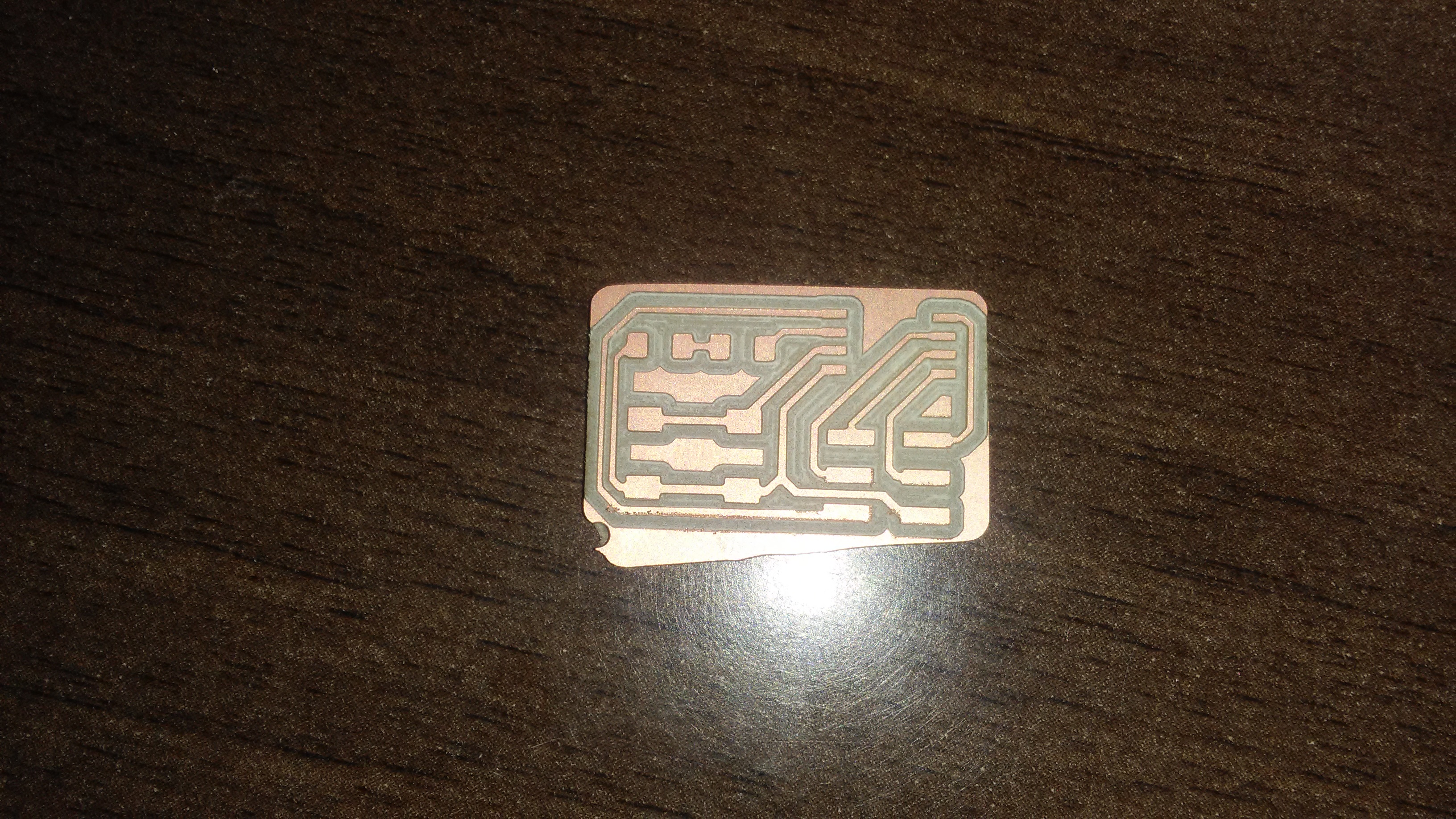
I continued to mill the board to create the desing I made.
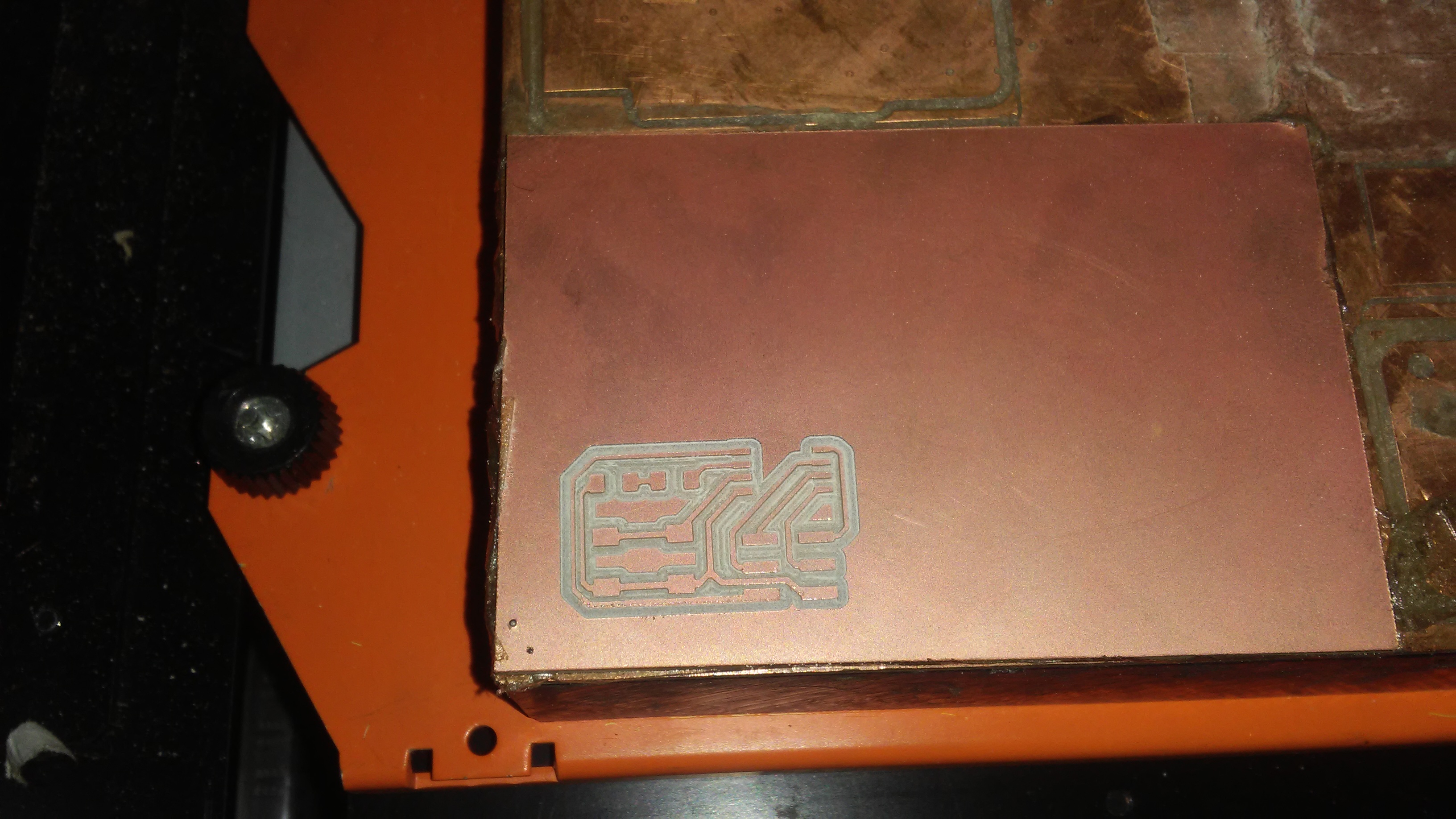
This is the final image of the board.
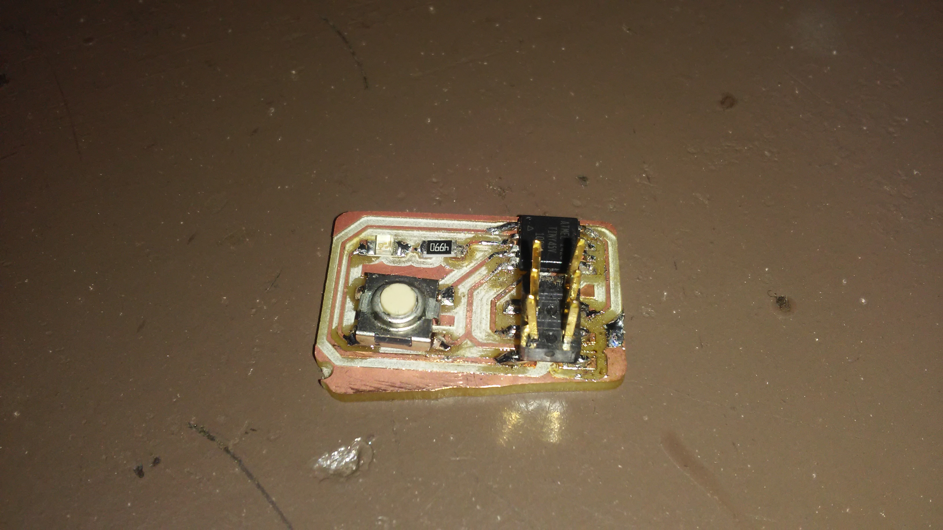
I soldered all component as listed below
| No | Componet | Pieces |
|---|---|---|
| 1 | ATtiny45 | 1 |
| 2 | Push button | 1 |
| 3 | LED | 1 |
| 4 | Resistor | 1 |
| 5 | AVR ISP | 1 |
Steps on how to solder component can be refered to week 4 assignment.
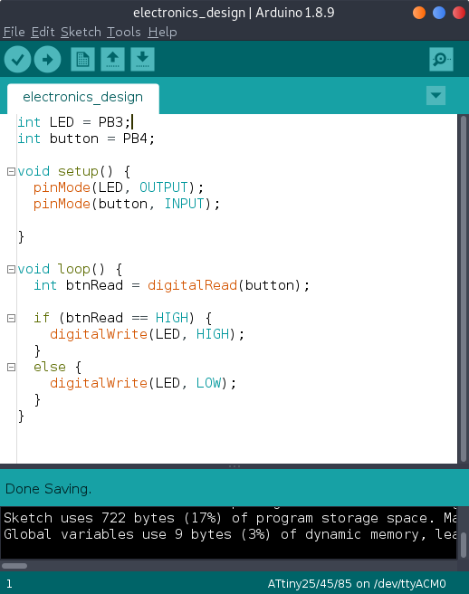
After I continued to program the board I just made to flash the LED when the push button is pressed.
This is the program I wrote.
On how to see the working circuit you can check on week 8 assignment.
Conclusion
Everything work perfect only when I was cutting the OUTLINE of the board its were it failed because the tape I was using to hold the board down wasn't strong enough and the board moved a bit and caused some issue on the look of the final board.
The original files used for this assignment can be downloaded here.