9. Embedded programming
This week was based on the how to program a ATTINY 44 board, which was made in the electronics design week with additional switch and light ,using different programs like “C”,arduino ide,etc.and by that glowing the LED by using an ON/OFF switch
The group project was to compare different architectures.
PROGRAMMING THE BOARD
1.The first step I did was to go through the designing week and estimate a brief idea about the various connections made.
2.The second thing I did was to download the Datasheet and went through the data sheet.
(i) From the Datasheet The basic architecture of ATTINY44 were referred
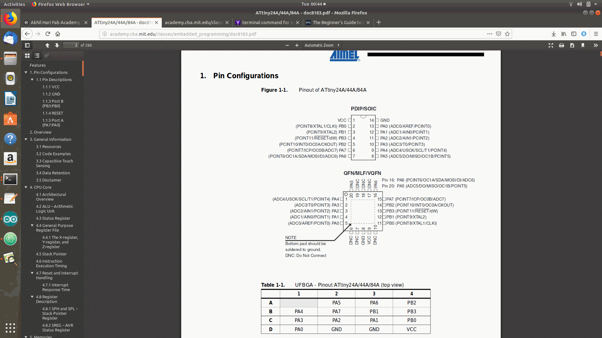
(ii)The pin configurations like vcc used for input voltage,Gnd as Ground,Rst as reset and the remaining 6 pins from port A and 6 pins fro Port with description were referred from the Datasheet.
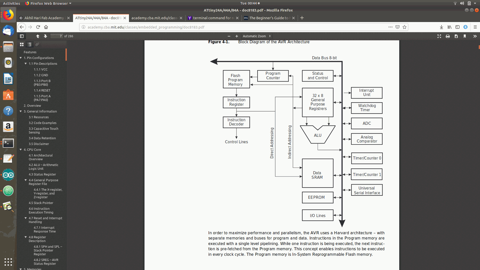
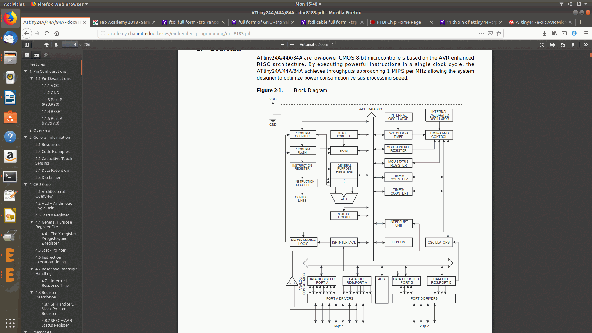
(iii)The Block Diagram of AVR Architecture were studied as if it consists of an 8 bit serial bus in which onside of the terminal consist of i/p of Comparator,WatchdogTimer,ADC,2Counter/Timers Etc and on the other side it consists of memory space like EEPROM,Data SRAM,ALU,General Purpose Registers ,Program Counters,Flash Memory,Instruction Registers and Instruction Decoders etc.
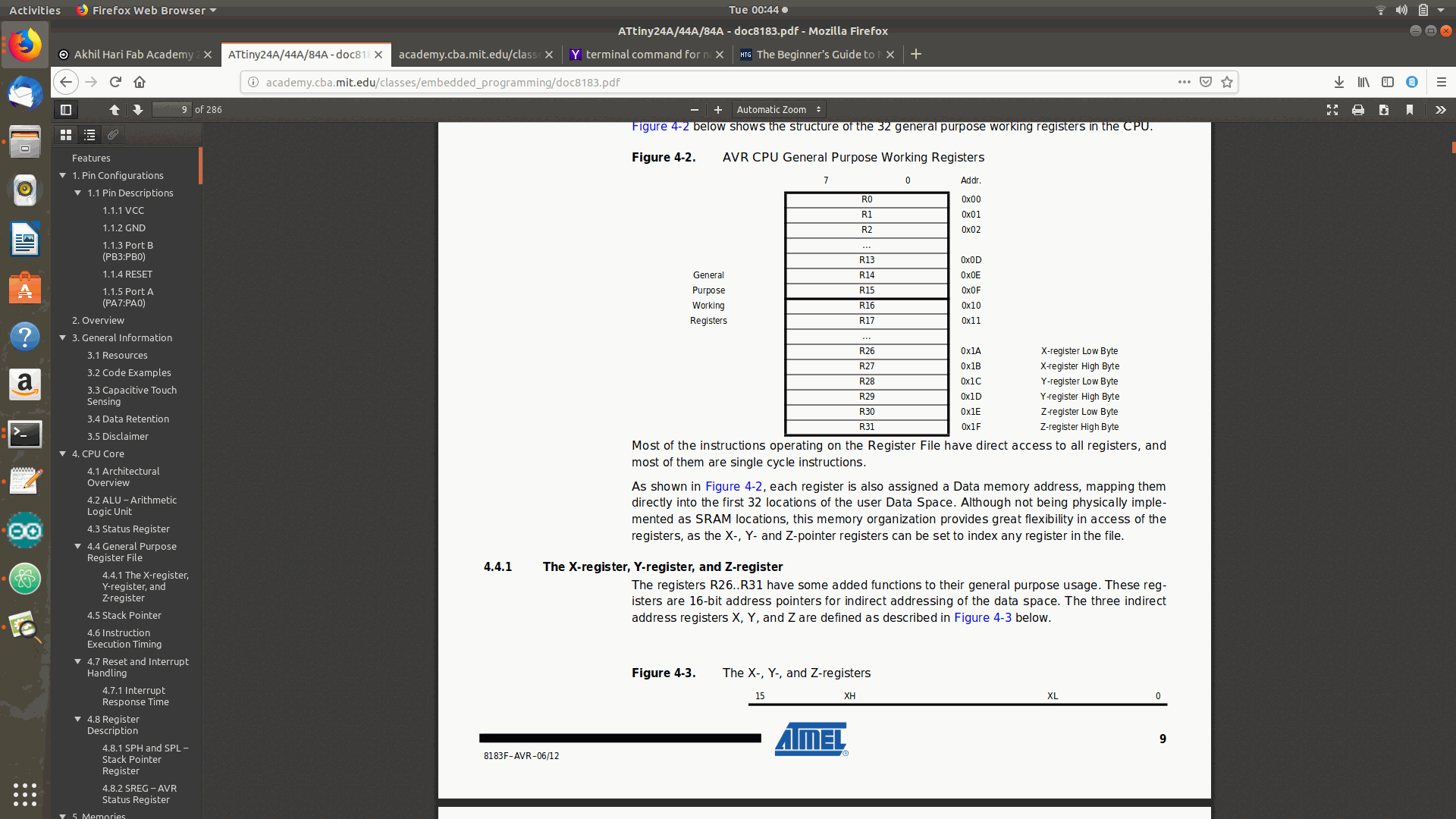
(iv)Then it consist of working of General purpose registers like it consist of allocations from R0-R31 with address starting from 000 till 01F
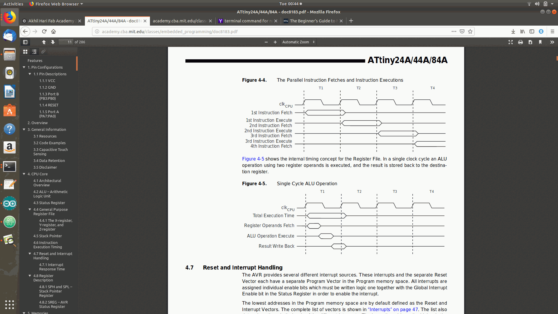
(v)Then I referred about the parallel instruction fetches and Instruction Executions and the single cycle ALU Operation.
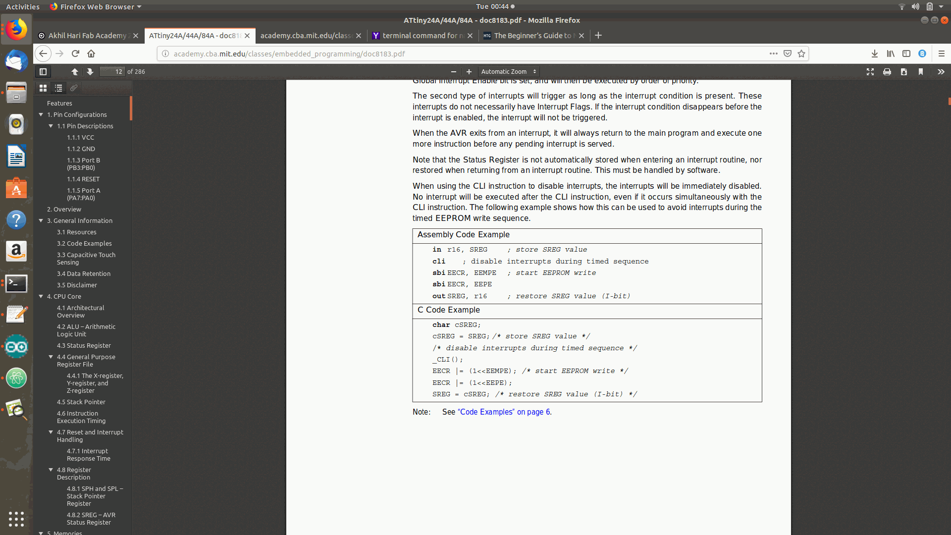
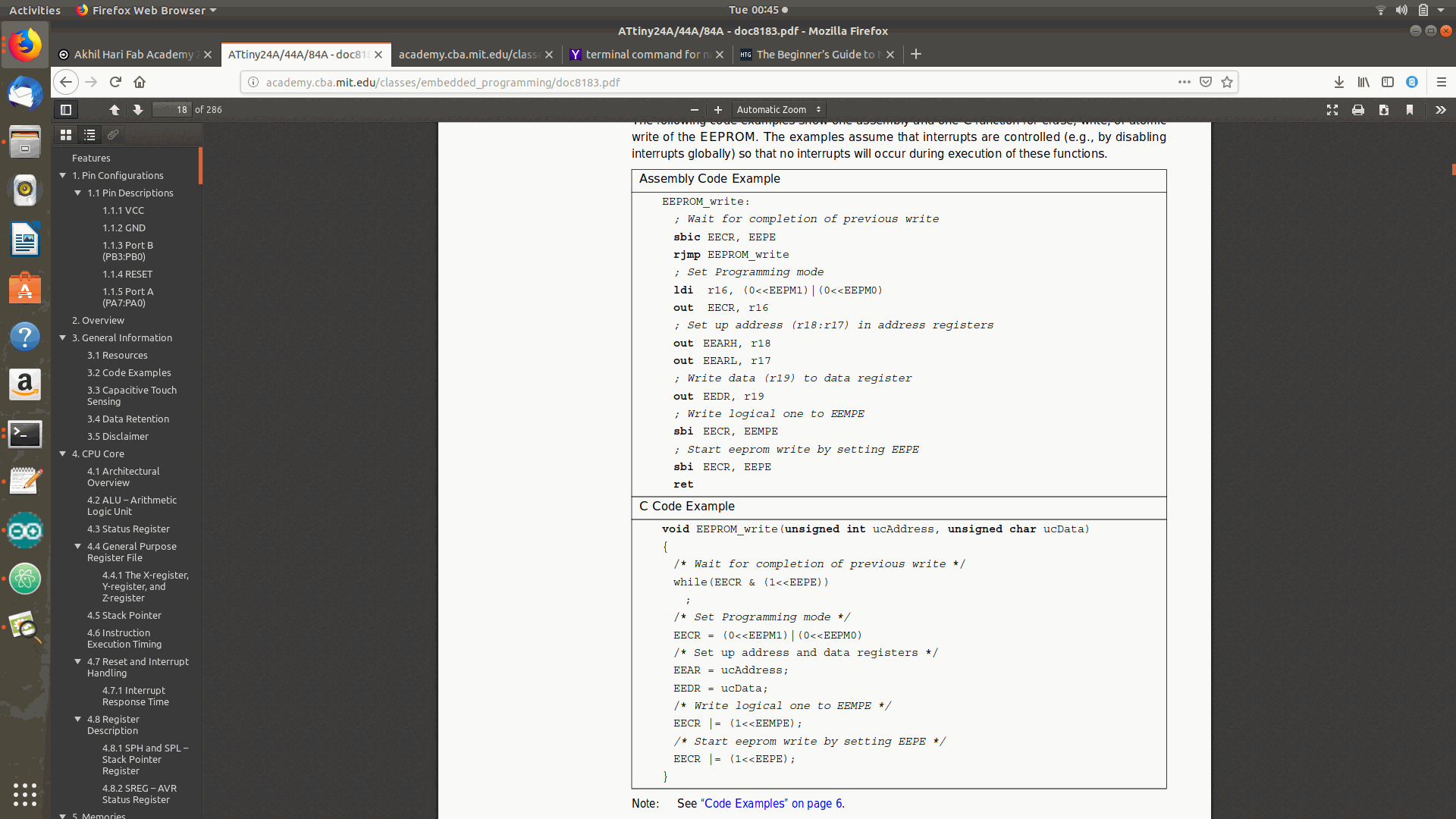
(vi)Then referred about the example for assembly code and the procedure for allocation of memory space ie in EEPROM and an example for C Code.
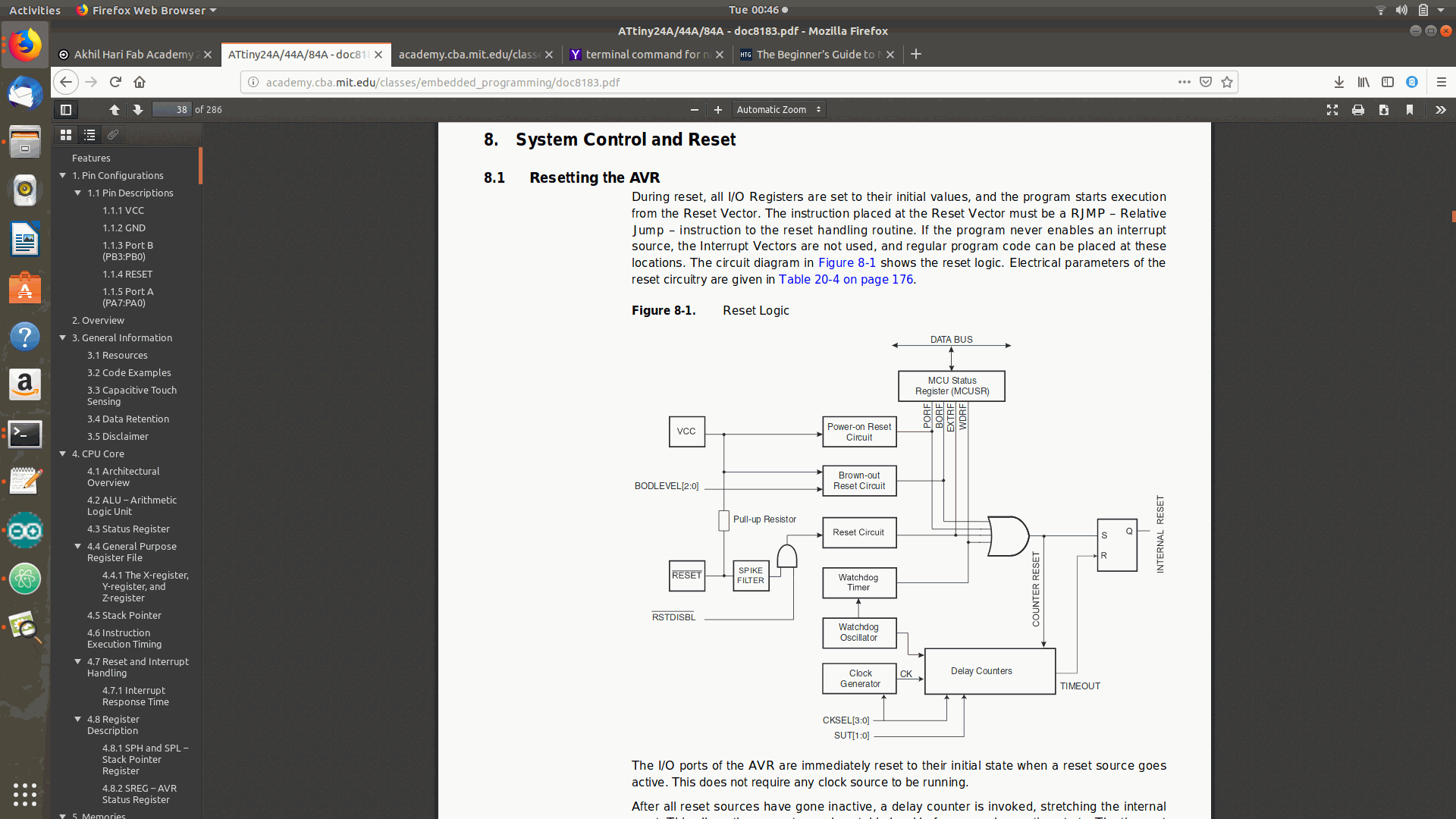
(vii)Then I went through the system control and reset ie Resetting the AVR ie the VCC is connected serially to power-on Reset circuit and parallel to the rest all other parts namely Reset,Spike Filter,Reset Circuits etc.and from that to delay counters and then to the gate signal followed by internal reset.
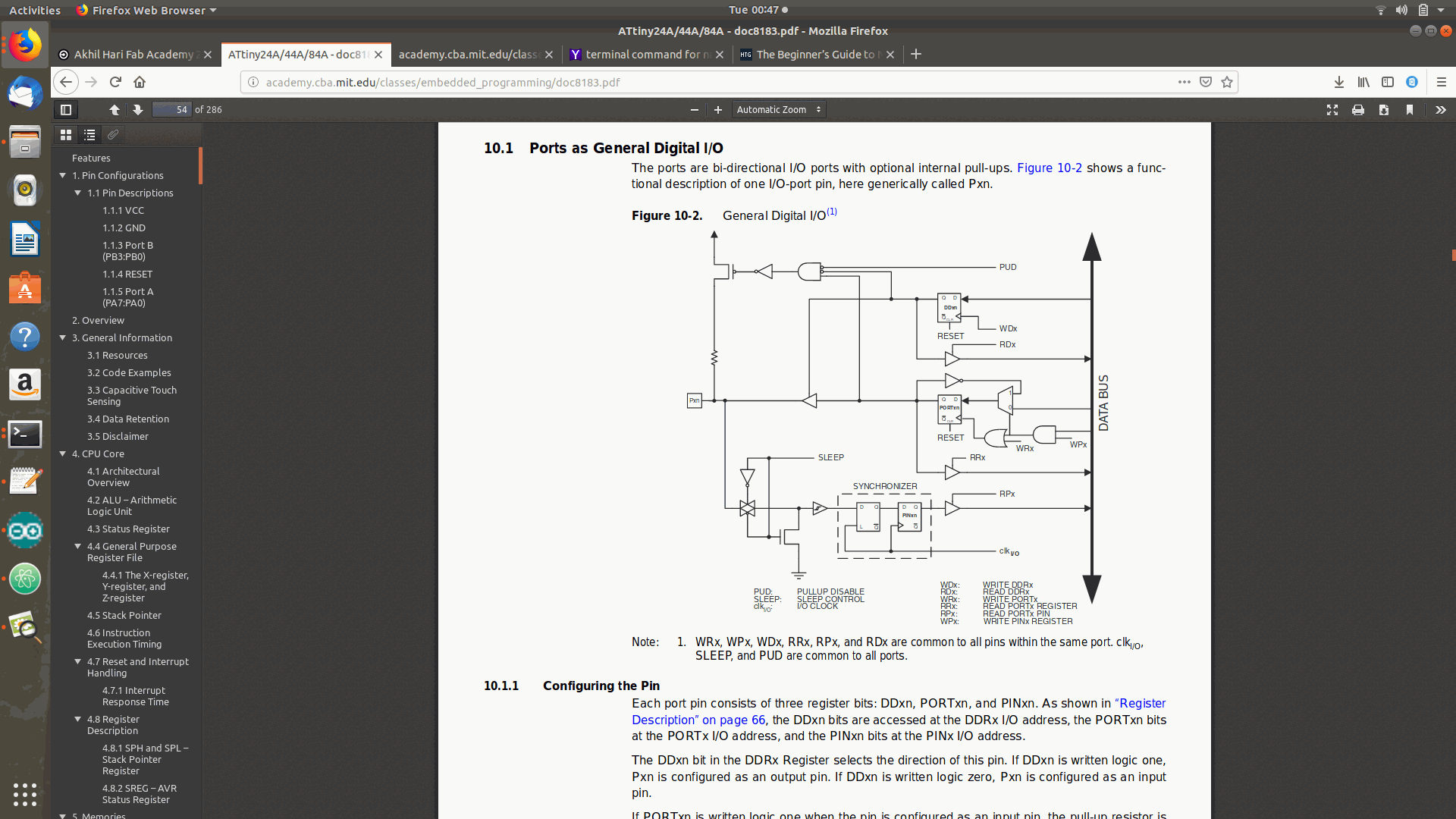
(viii)After that I referred about the input and output port architectures.
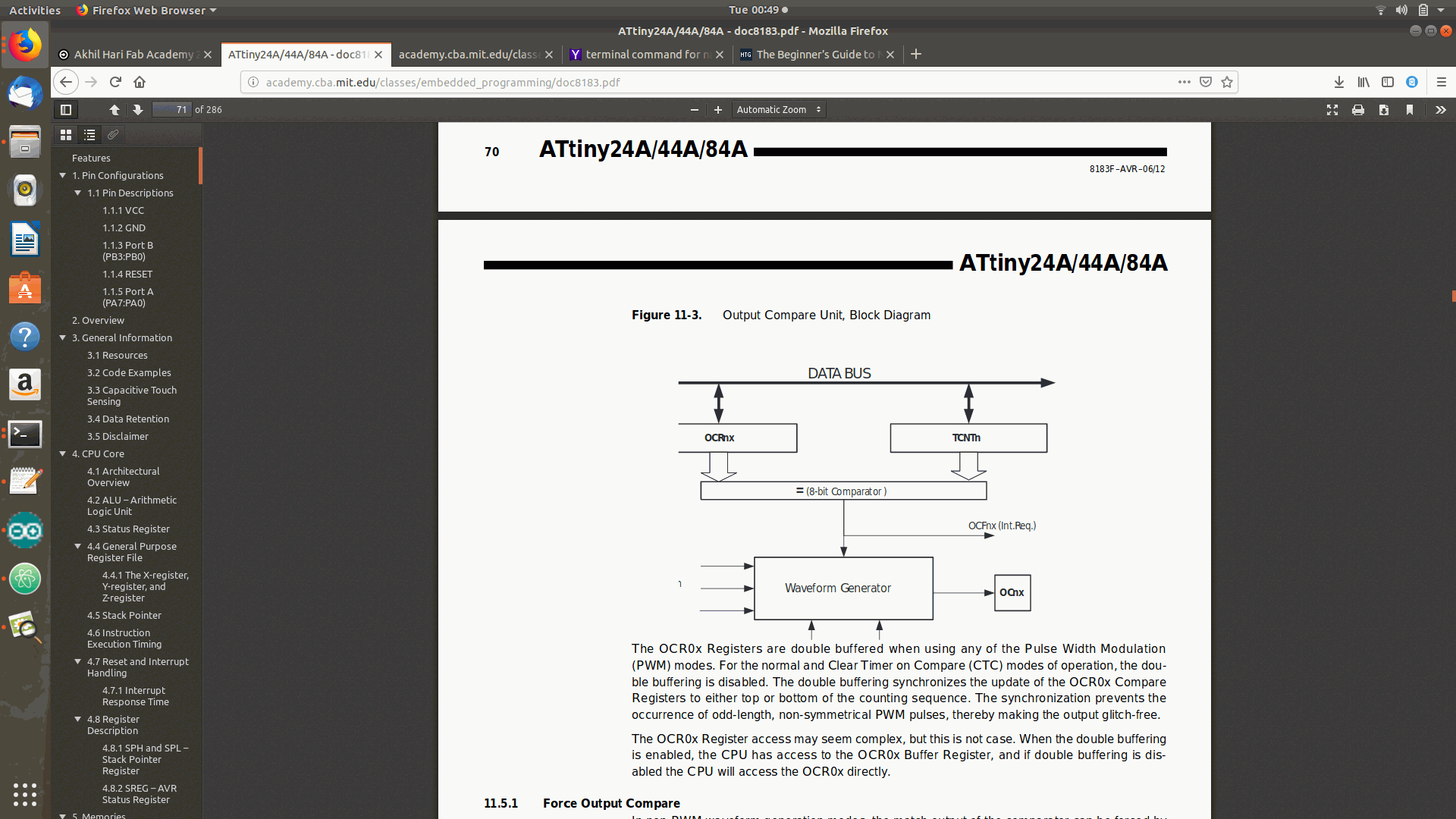
 (iX)Then I went through the DATA BUS Connection system ie regarding the comparator and waveform generator but it was not that much clear and the only thing I understood was it consist of a comparator to compare different inputs and give outputs.
 3.Then studied some of the basics of c++ from the tutorial site.ie regarding header file,body,what is data encapsulation,data protection,loops especially while and else loop etc.
LED PROGRAMMING
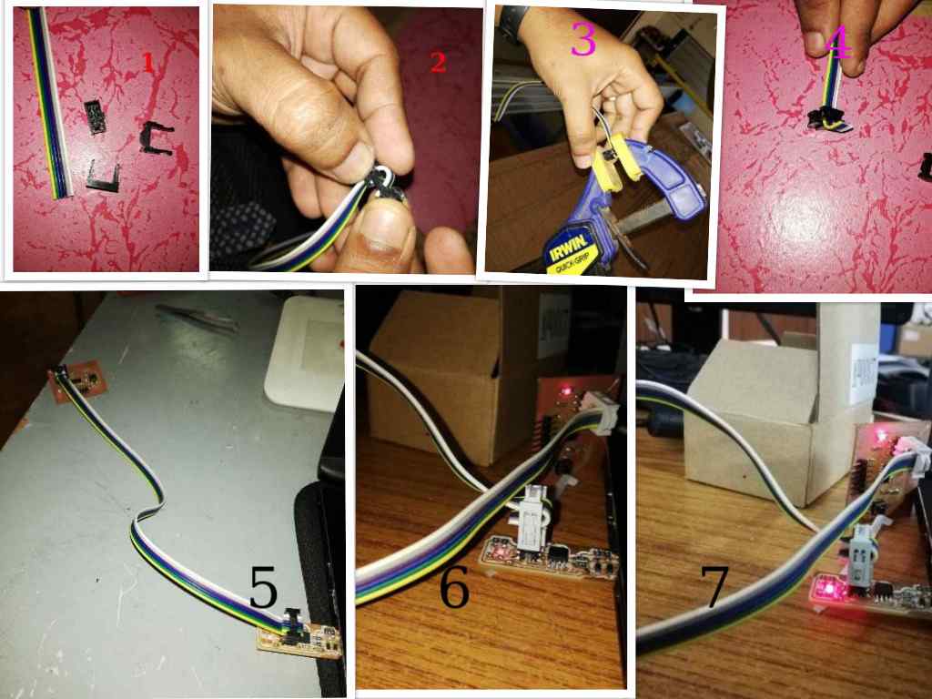
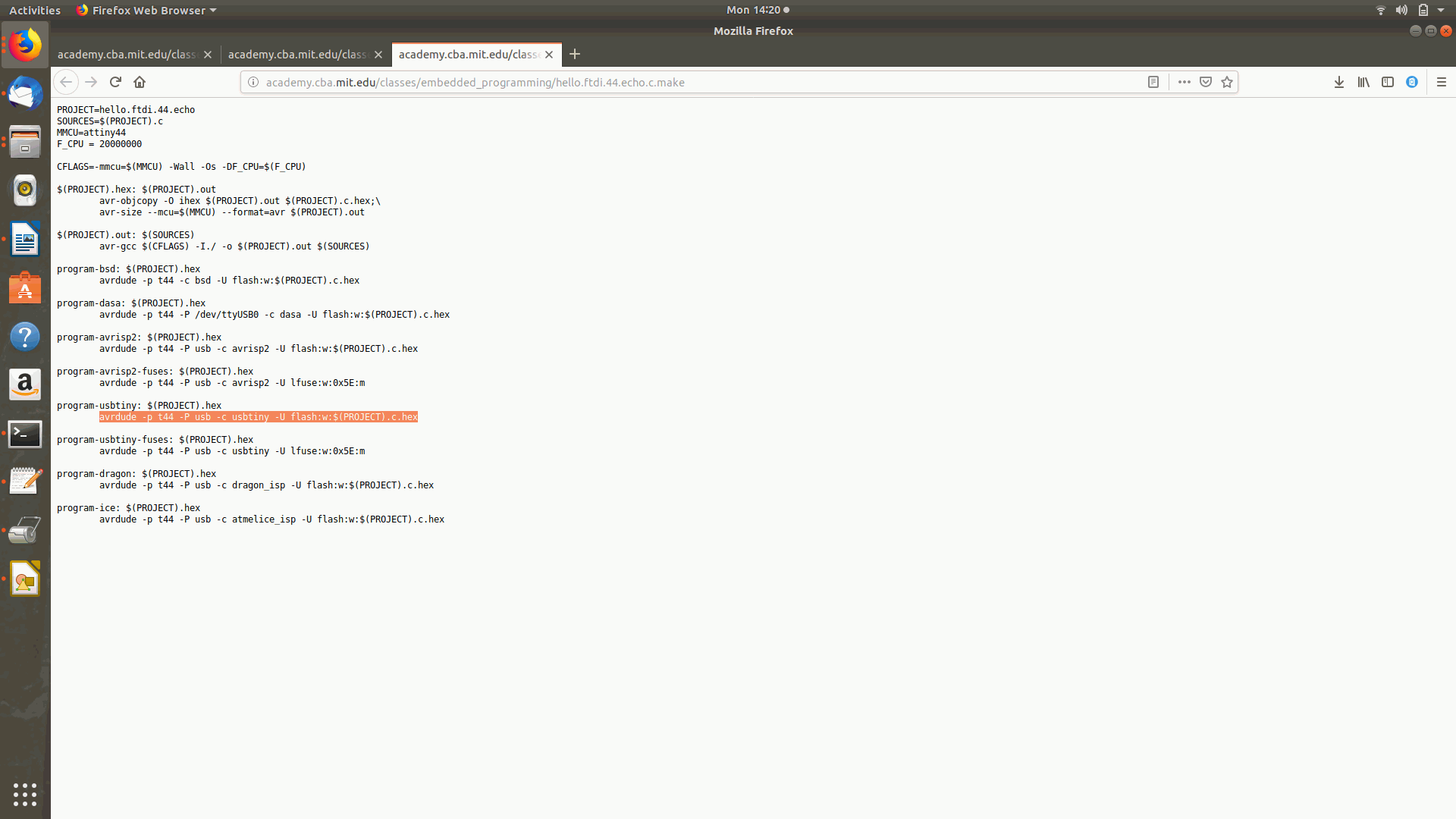
1.Instructor also helped to study the basics like header,objects,loops etc.and he also passed a sample document of make file and connected the designed programmer and the board to the PC by using six pin wire connector which was made by using idc header pin
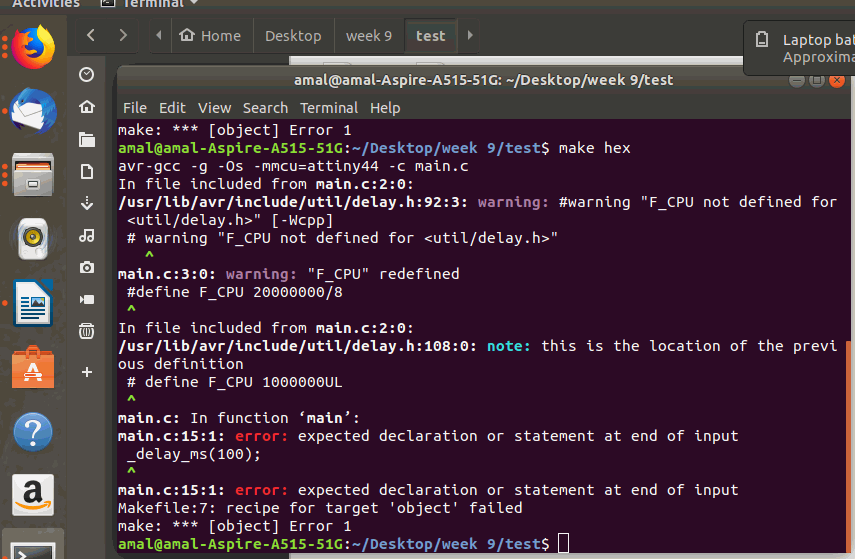
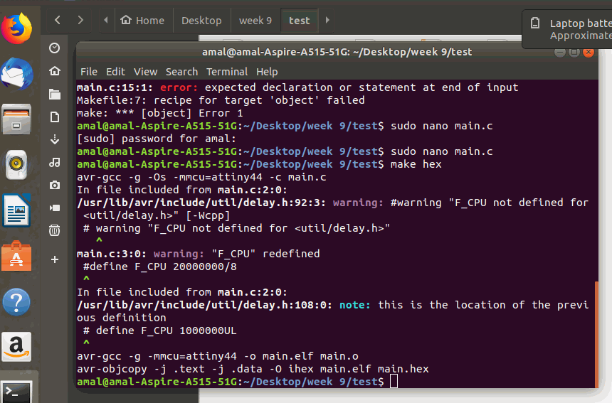
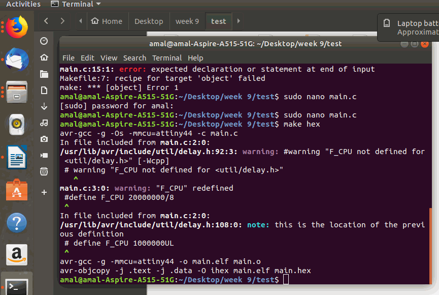
2.After creating a file the makefile document was passed and defined the header and the F-CPU value as 20000000 and divided it by 8 for simplifying and performing one operation was declared and the by using the following commands the hex file was made
        object:

        link:
     avr-gcc -g -mmcu=$(device) -o $(file_name).elf $(file_name).o

    hex file:
 avr-objcopy -j .text -j .data -O ihex $(file_name).elf $(file_name).hex
and the hex file was made by using the commands
hex: object link hex file
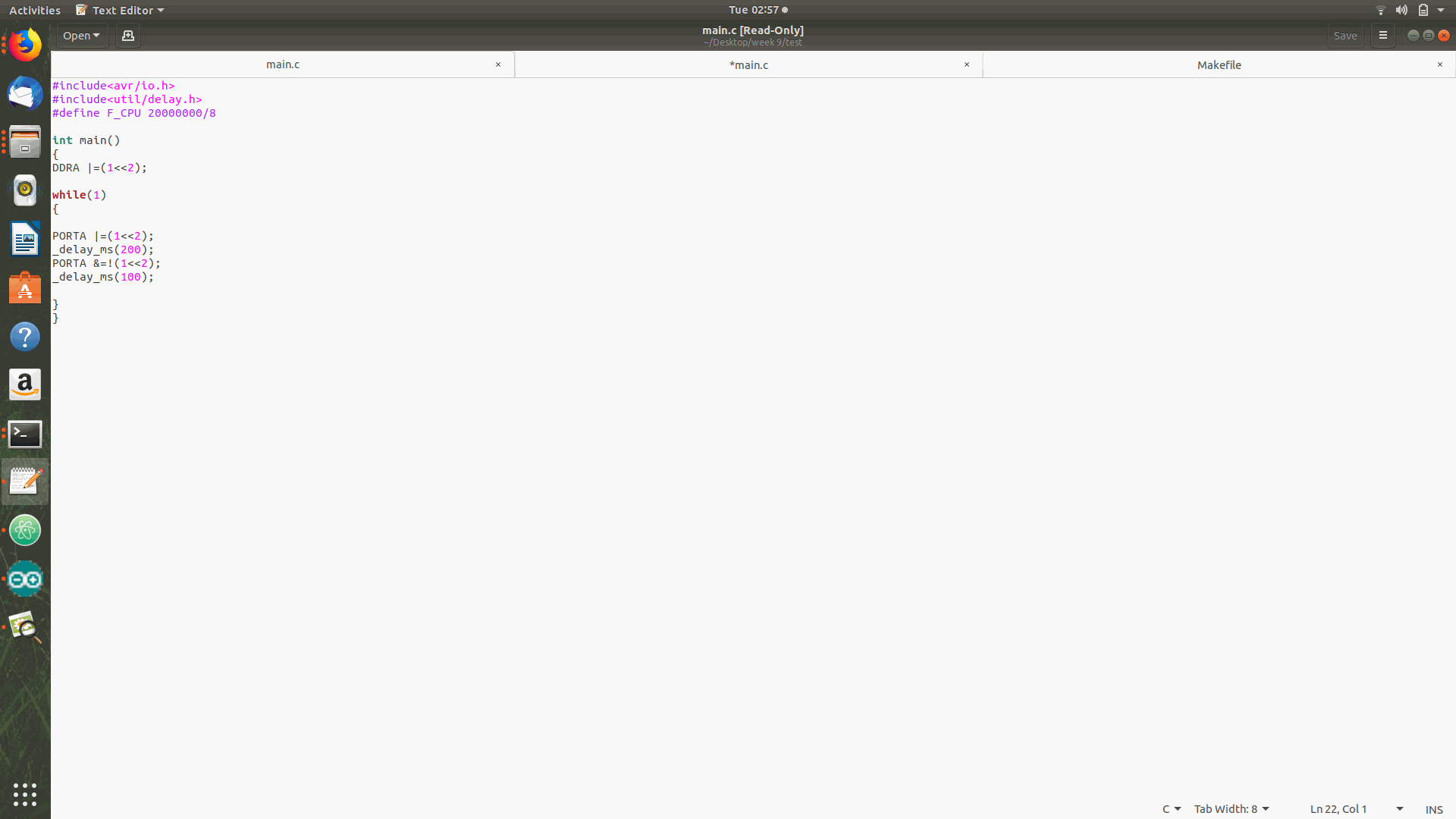
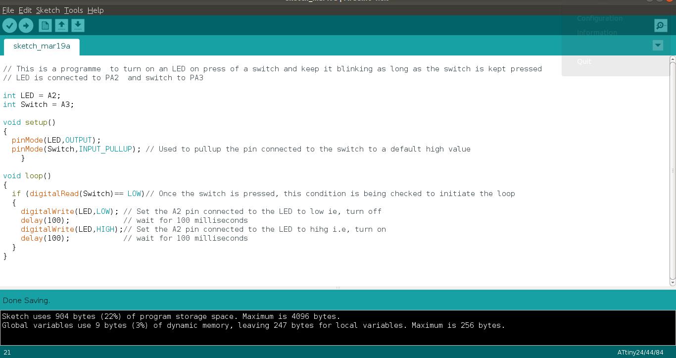
3.Then by using a simple text editor the c program for lighting the led was programmed and while referring the circuit it was noted that LED was connected to NS$1 which is the 11th pin of ATTINY44 and the c program was written based on that.
             #include<avr/io.h                           (Header)
             #include<util/delay.h>                      (Setting the delay from library)''
             #define F_CPU 20000000/8                    (Defining the CPU Cloak)''

                int main()                                   (Basic Body starts and this is the point were operation begins)
                {                                            (Opened the command opening braces)
                DDRA |=(1<<2);                               (Data direction register showing the port with PA2 position)

                while(1)                                     (Declaring the loop)
                {

                PORTA |=(1<<2);                               (Operating the while loop)
                delay_ms(200);
                PORTA &=!(1<<2);
                delay_ms(100);                               (setting the delay)

                }                                             (Closing the loop)

                }                                                                                  (Closing the body)'
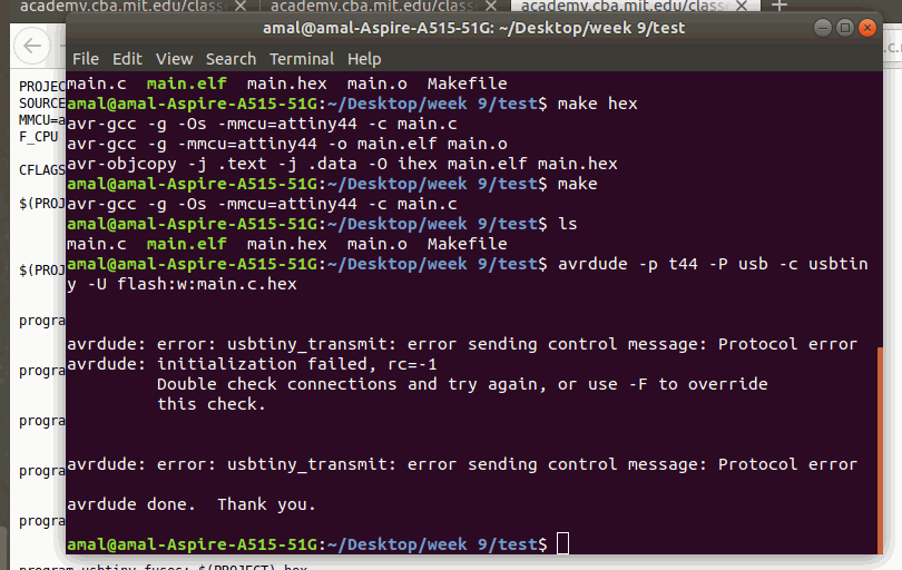
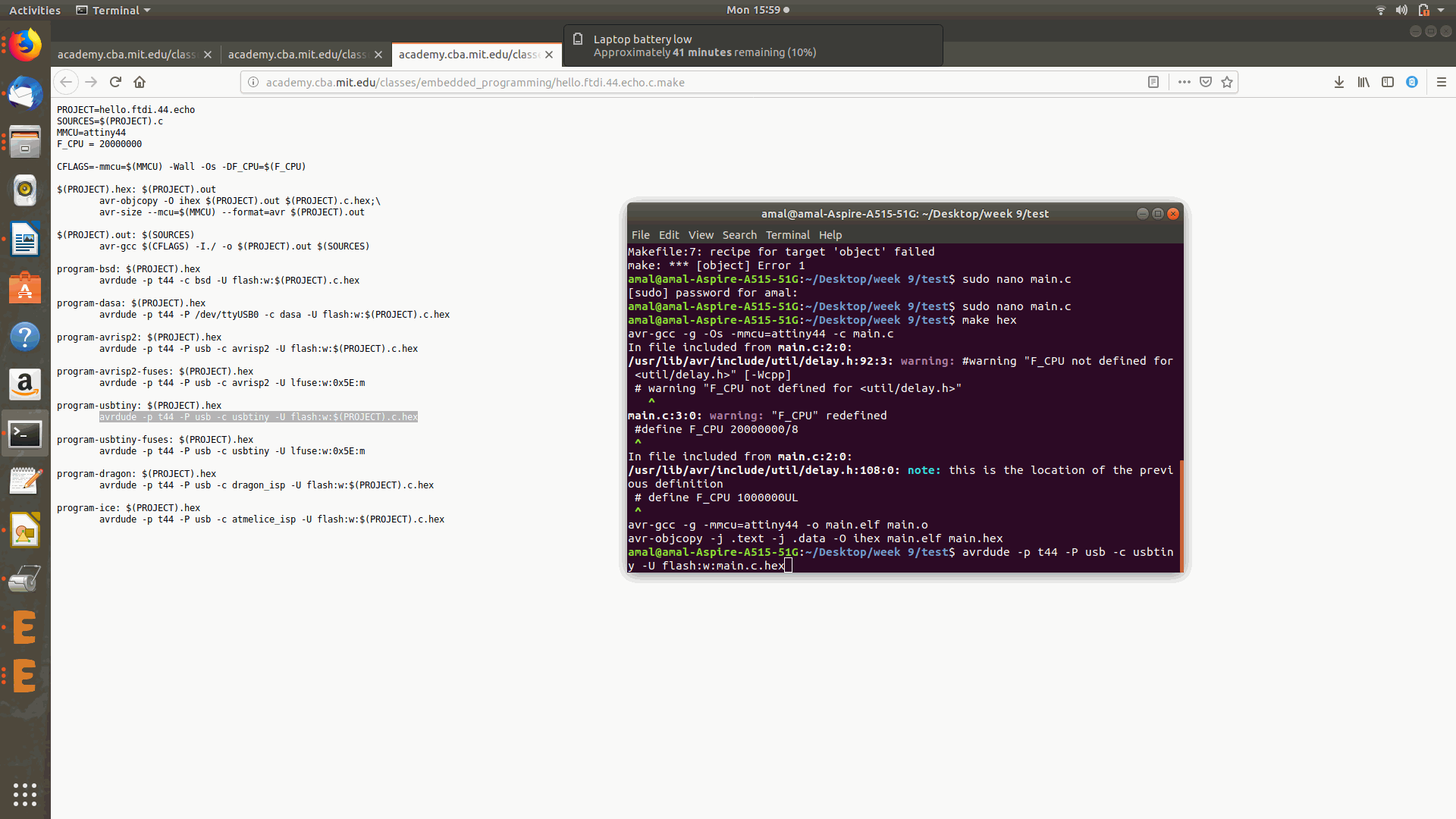
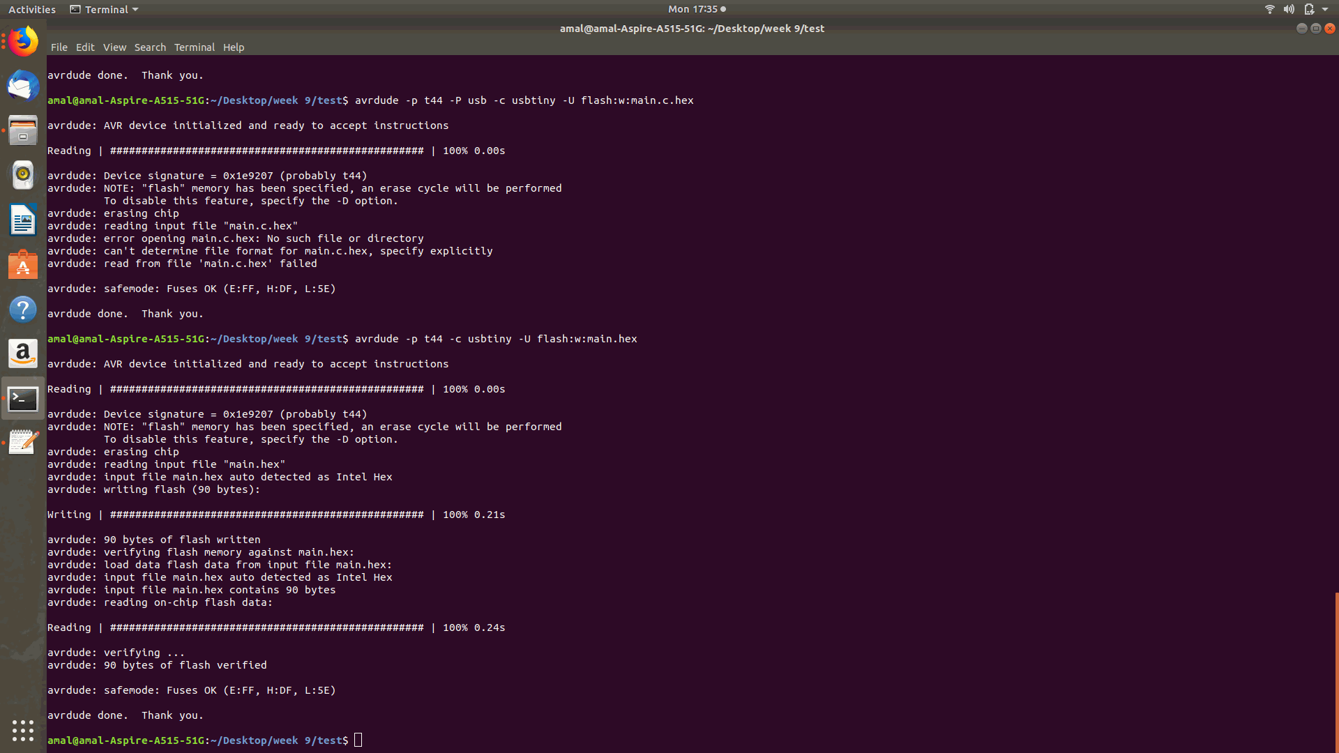
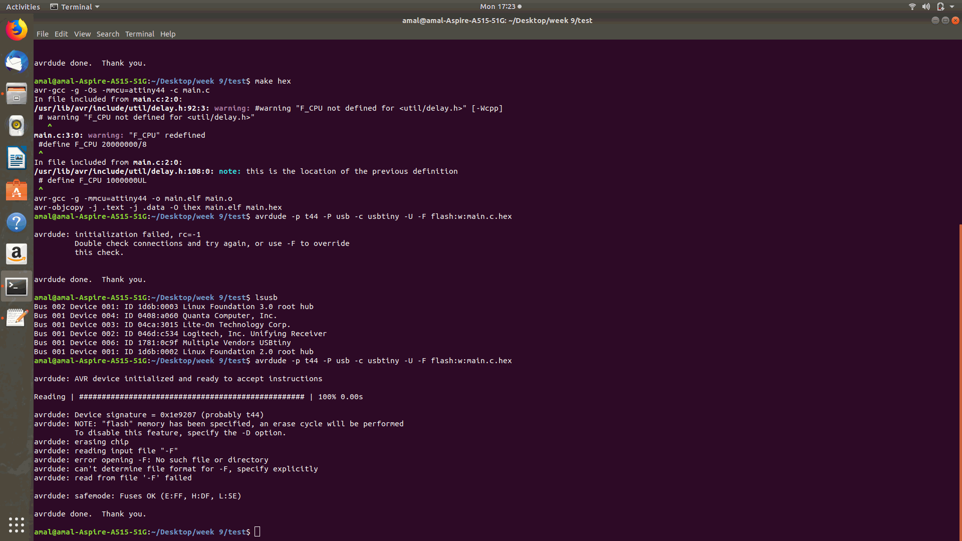
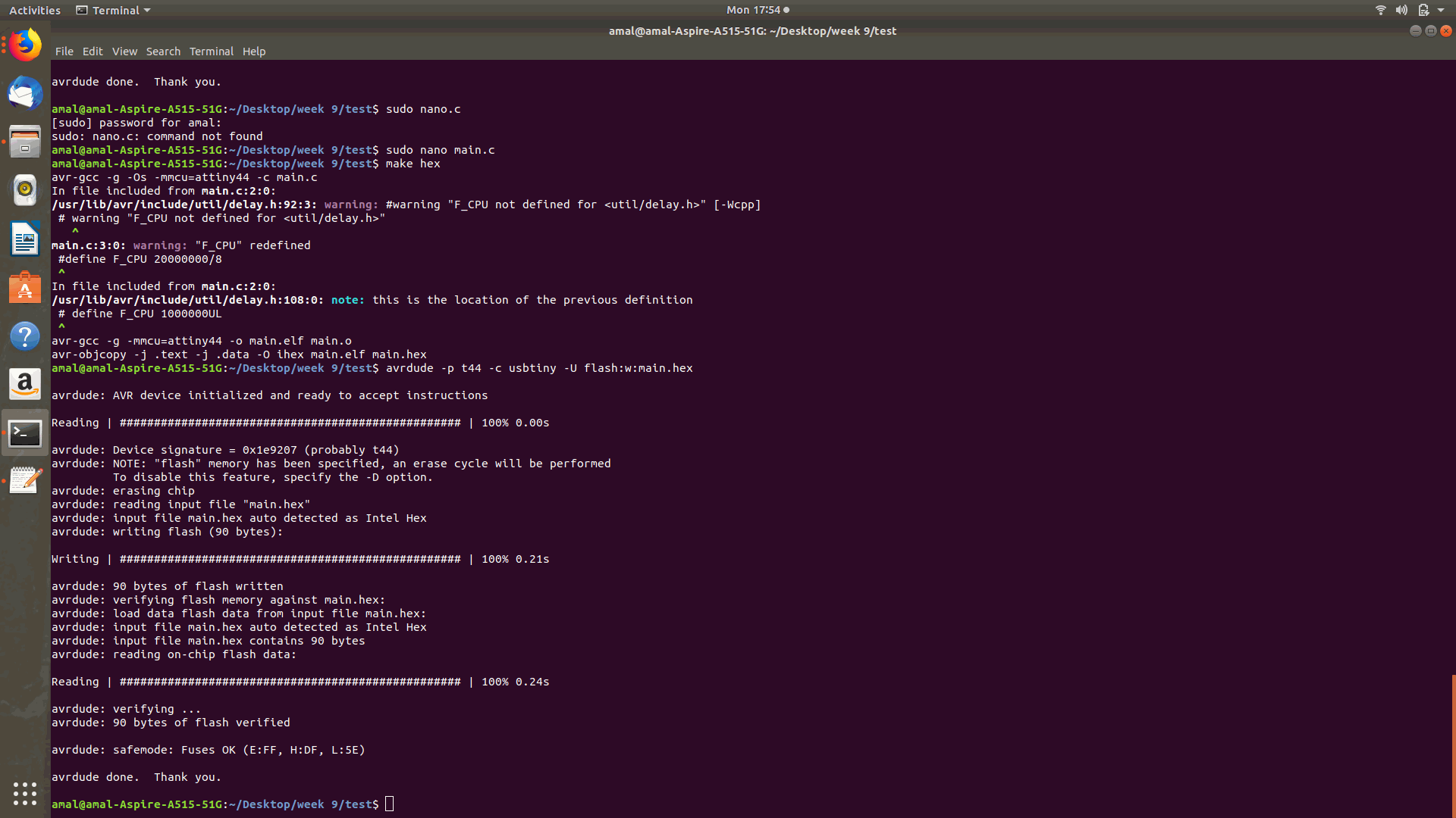
- Then the File interface was made by using the command Avrdude from the academy site.
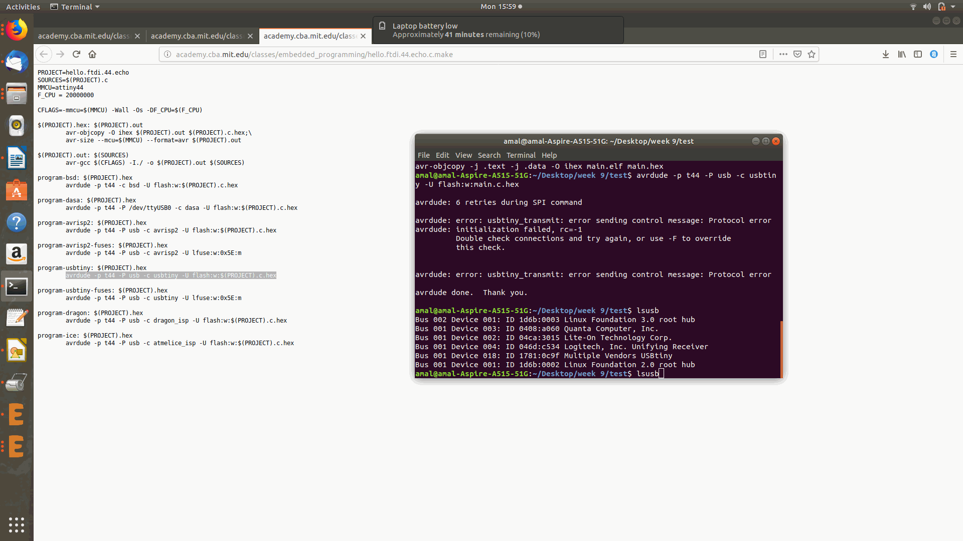
5.Then made the hex file and even checked the program by using micro second delay of 100ms and 500ms.
After that the arduino ide was installed in ubuntu using terminal.

After that I opened up the fresh page of arduino IDE
After selecting the board specifications by downloading the minicore file from
“https://mcudude.github.io/MiniCore/package_MCUdude_MiniCore_index.json”
by adding preferences from the file dropdown menu Arduino Ide,I burned the boot loader.
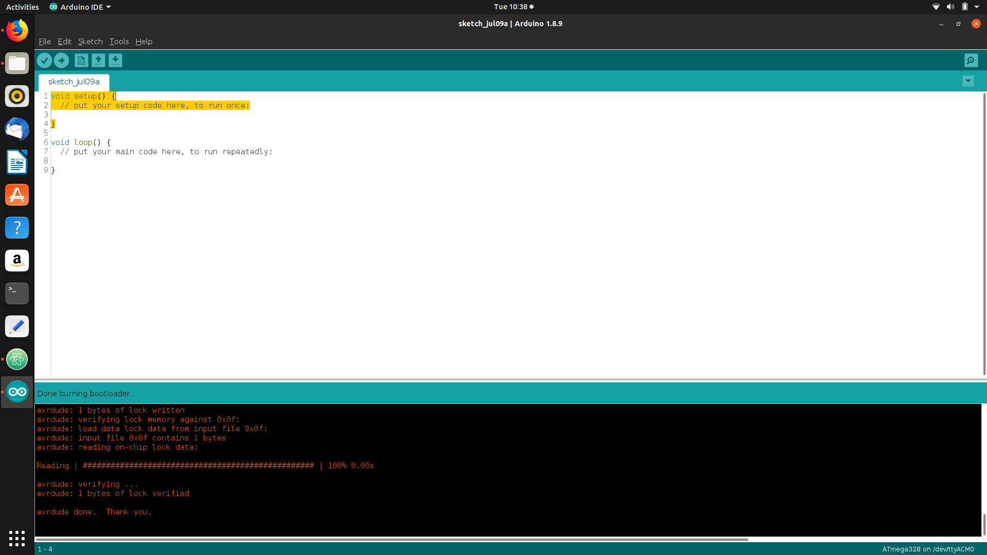
After that I entered the program ,saved and then uploaded the program.
VIDEO
CLICK HERE TO DOWNLOAD THE VIDEO
GROUP assignments
The group assignment was to Compare the performance and development workflows for other architectures
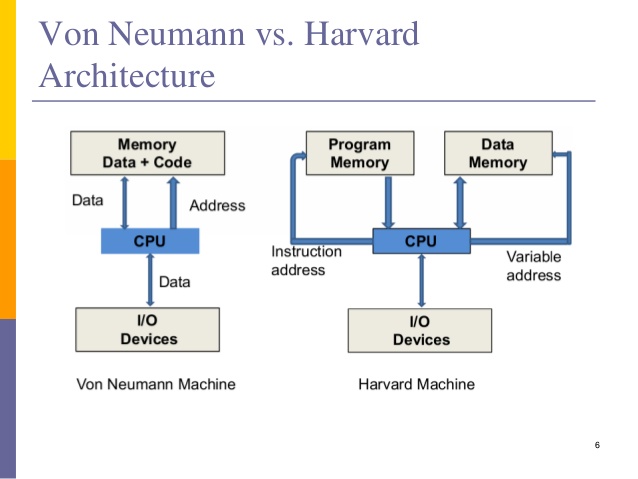
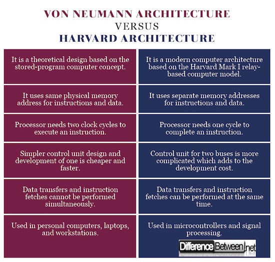
For that I started with the architectures of Harvard and von Neumann
Basically every embedded system is divided into two architectures Harvard and von Neumann
The difference between has been stated below.
(credits:https://www.google.com/search?client=ubuntu&channel=fs&tbm=isch&sa=1&ei=OCgkXcjXBsSm9QPx2KmQBA&q=comparison+between+von+neumann+architecture+and+modified+harvard+architecture&oq=comparison+between+von+neumann+architecture+and+mod&gs_l=img.1.0.35i39.14360.34433..36512…6.0..0.336.6118.28j29j0j1......0....1..gws-wiz-img.....0..0j0i67j0i8i30j0i24.rBD6KTgUNPk#imgrc=ody1mrVlnCo8CM:)
It is understood that the VON NUEMANN architecture serves the memory allocation is mixed ie.the memory for data and code is mixed and while in the HARWARD architecture the code and data has different memory allocation.
A Von Neumann architecture has only one bus which is used for both data transfers and instruction fetches, and therefore data transfers and instruction fetches must be scheduled - they can not be performed at the same time. It is possible to have two separate memory systems for a Harvard architecture.
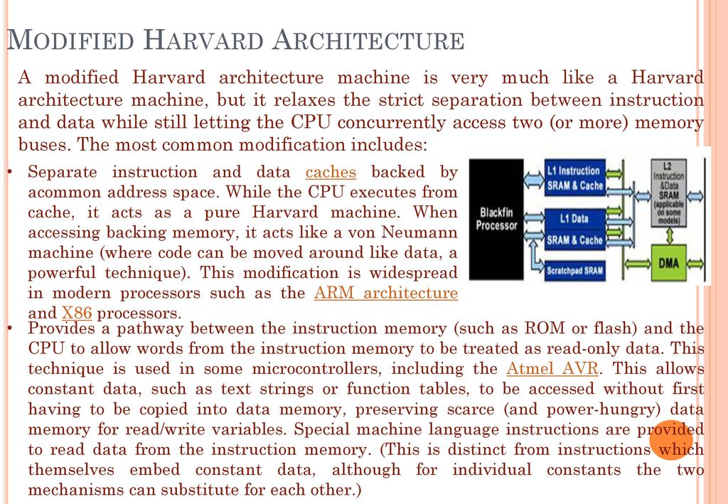
Modified Harvard Architecture