7. Electronics design
Assignment 1- Individual
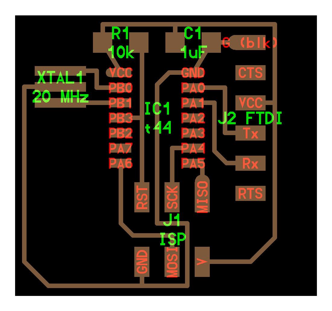
This week the aim was to redesign the Helloworldboard by adding a switch and an LED. Without having a pre knowledge in electronic circuits, my lab instructor helped us with the fundamentals of pull up and pull down resistors in circuits.
 This board has to be redrawn

A pull up resistor
The design of the circuit and trace was done on Autodesk Eagle Software.
Steps in design
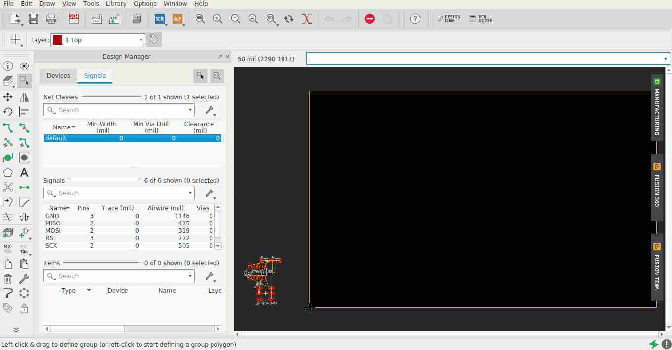
Working in EAGLE
-
Prepare the schematic file of the circuit using the connections shown in the board. Eagle has an elaborate library of the components.The library was downloaded from fab. Following items are added
-
ATTINY44-SSU (ATTINY44) (Package:SOIC14, Library: fab)
- Resonator (Package:EFOBM, Library: fab)
- Resistors - RES-US1206FAB (RES-US) (Package:R1206FAB, Library: fab). Two resistors are of 10k and the thrid one is of 499 Ohm. Resistor R2 (499) is used as the current limiting resistor for the LED and R3 (10k) is the pull up resistor.
- LED(Package:LED1206 , Library: fab)
- MM_SWITCH6MM_SWITCH (6MM_SWITCH) (Package:6MM_SWITCH, Library: fab)
- FTDI-SMD-HEADER (Package:1X06SMD, Library: fab)
- PINHD-2X3-SMD (Package:2X03SMD, Library: fab)
- CAP-UNPOLARIZEDFAB (CAP-UNPOLARIZED) (Package:C1206FAB, Library: fab)
Following commands in the command dialogue box are used to design the schematic
Net - To draw the connections
Name - To name the connections to connect them.
Move - To move the components.
After connecting ERC or Electrical Rule Check has to performed to ensure whether our connections are proper. The software will check for basic circuit rules like Kirchoff’s rule etc.
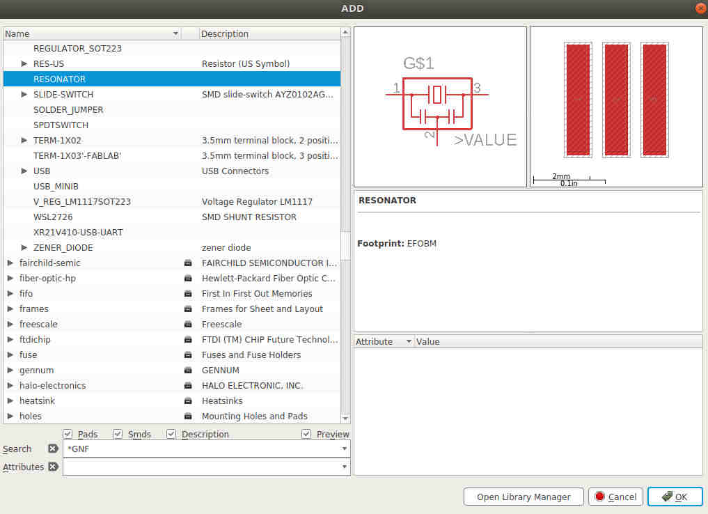 Library
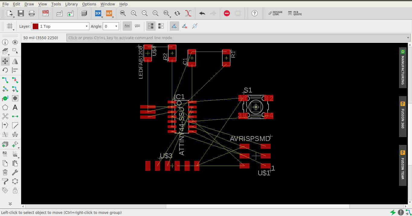
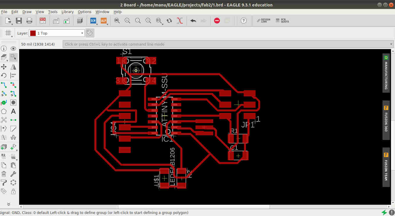
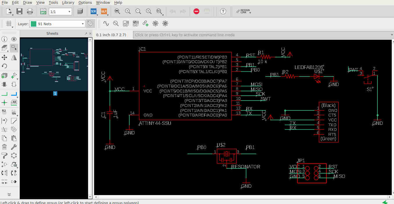 Schematic after adding the components and connecting them.
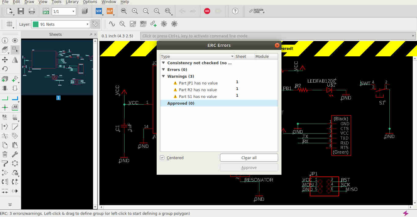 ERC check
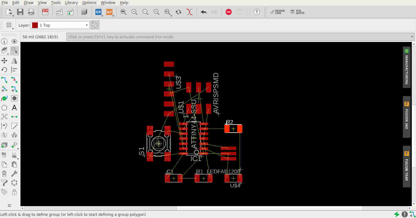
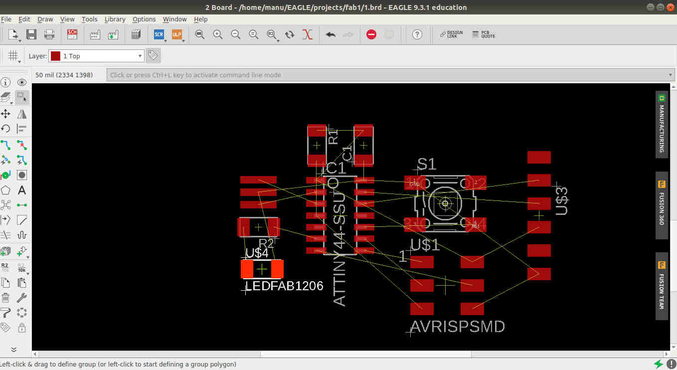
- Switch to board to start making the circuit. Here after arranging the components and the connections, auto routing was run to get the best route.
Before running the auto route, the Design rule Check/DRC has to be fixed. Here we fix the design rules for the ciruit board.
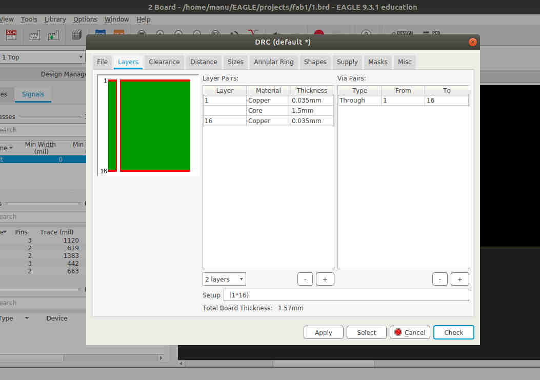
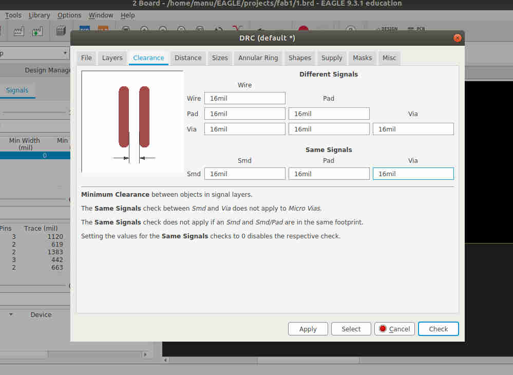 Clearance between traces are adjusted to 16 mil. 16 mil is almost equal to .4mm. This value was found in our group project on week 05, where we experimented with possible values for trace widths and trace clearances.
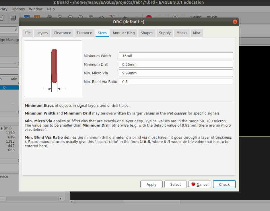 Minimum width of the trace as 16 mil
 Components in the lower corner are to dragged and placed in the drak screen to fix the circuits.
 Trial 1
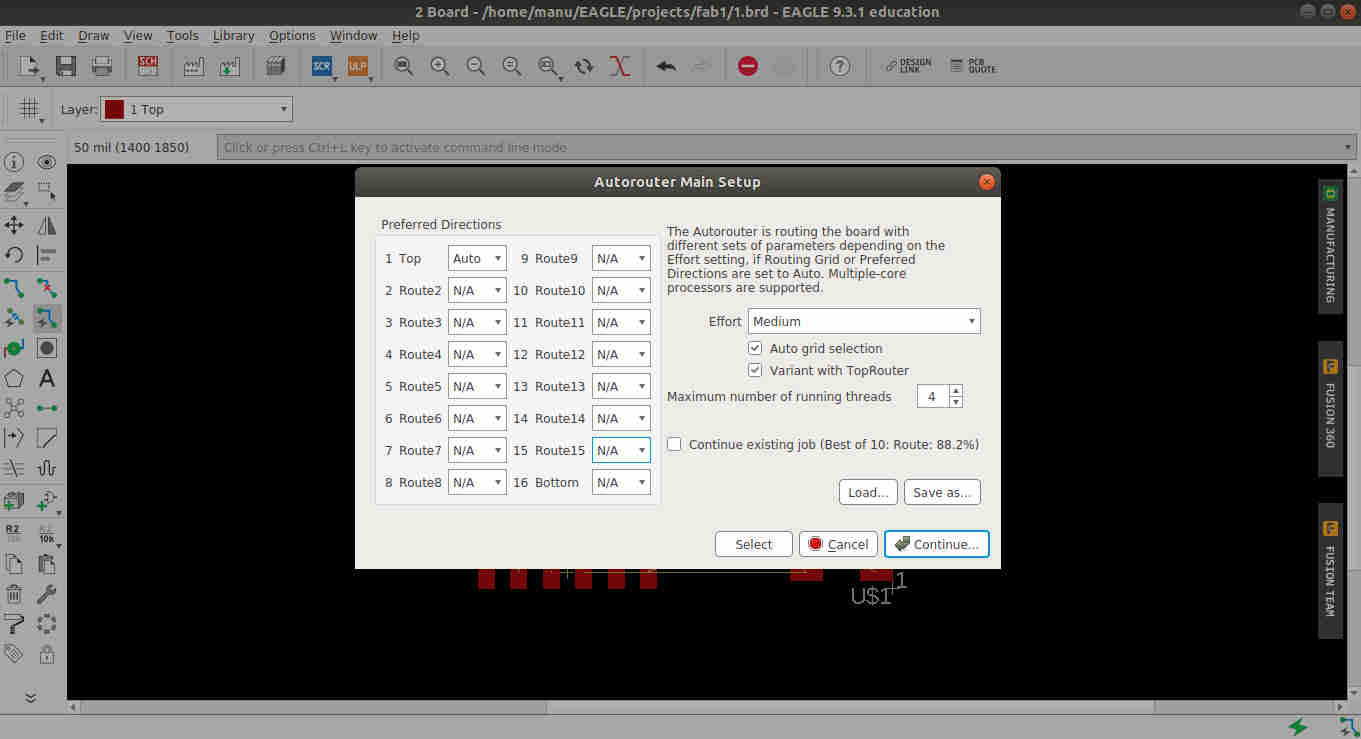 Auto Route dialogue box
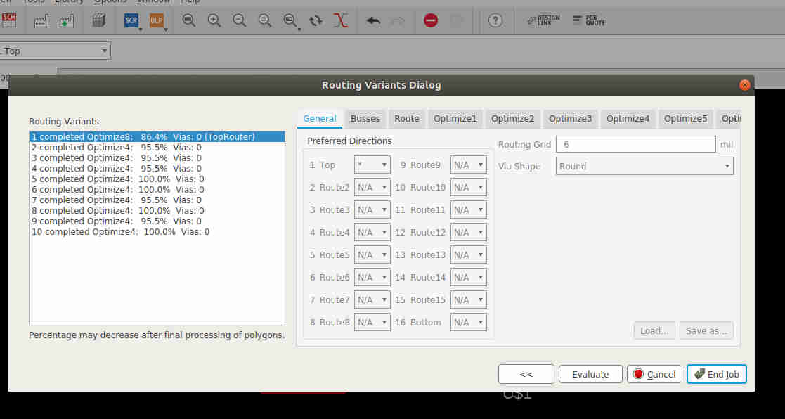 Autorouting in progress
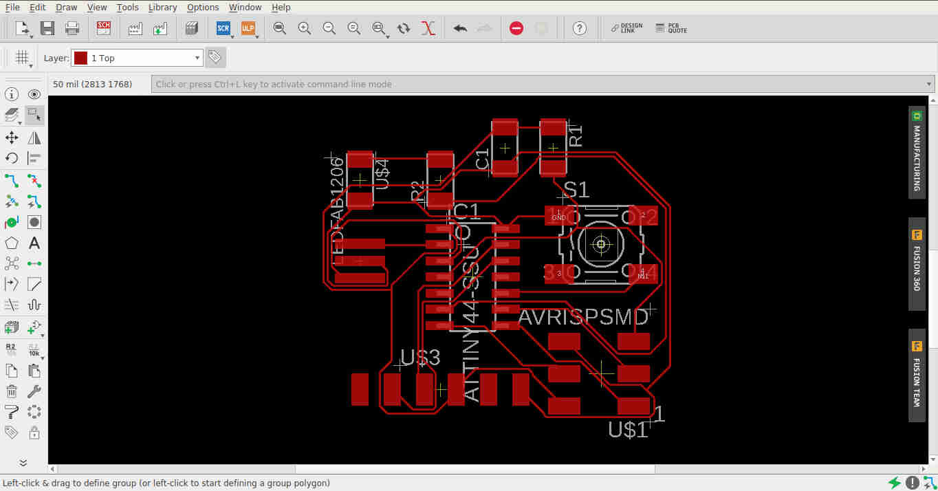
 Trial 1- After auto routing we can see that many connections(in yellow) are to be fixed without cross connection.
 This time the auto routing worked, but the DRC was set with minimum trace width.
 Trial 3
 Trial 3 - This time too with an error! and an attempt was made to bring the components a bit more closer.
 Trial 4, Unfortuantely that too was not optimised. I forgot to screenprint the finished trace path !
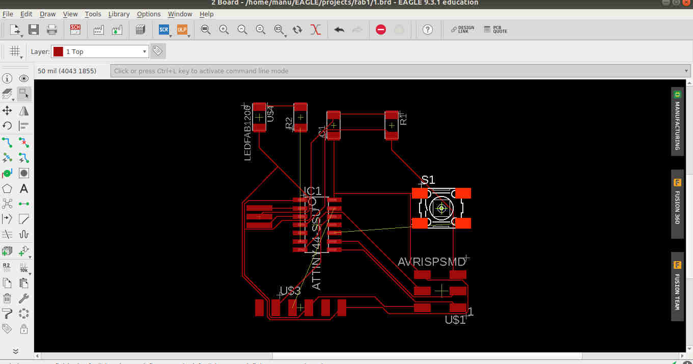
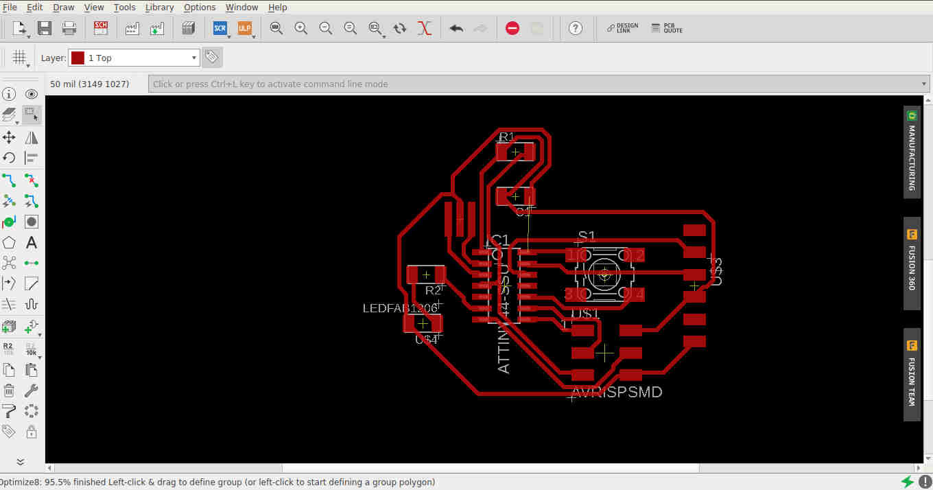
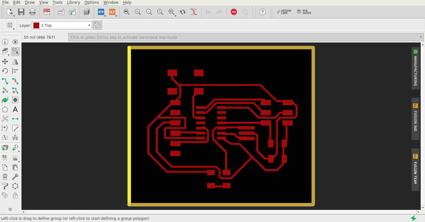
 Finally fixed with trial 5, a minor tweaking was necessary to get the final board.
Auto routing is always a good option, but manual routing is the best way. Here the route was fixed with auto routing and minor tweaking was done at the end manually. Let’s see if it works!
To print the PCB we need both trace and outer image of the board in png monochrome format at 1000 dpi resolution atleast.
This can be acheived by using the Layer command to turn on the top layer and keeping all other layers off to get the needed images.
 Turning on both top and dimension layers.
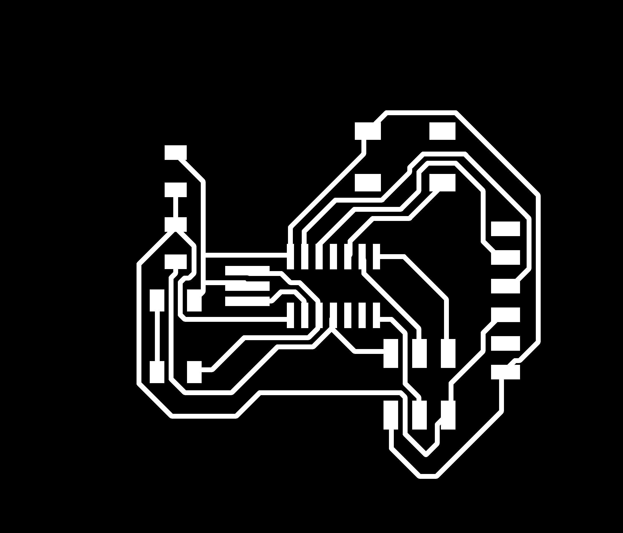
Trace outer
Trace inner
Files here
Milling the PCB
Using the exported images the PCB is milled in Roland MX-20 mill machine.
Traces are milled with V bit (1/64) and outer using 1/32 end mill.
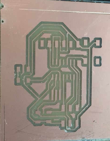
After milling. The edges are jagged and cutting incomplete as the 1/32 bit broke in between.
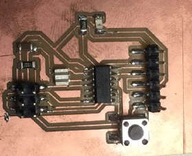
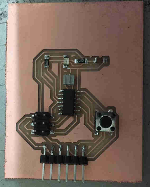
PCB after soldering The circuit was tested using a multimeter to check the connections.
Issues
-
It was found after soldering that the VCC pin and GND pin in the ISP header is interchanged. The circuit was designed properly, however I presume that the slots in the ISP female pin would have to be interchanged to match it. The best solution was to solder with a jumper wire to change the VCC and GND part after cutting the trace in the PCB to match the connection.
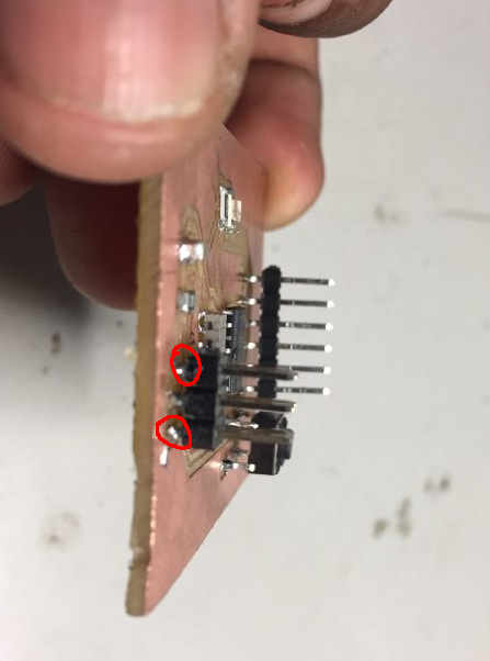
Points where connections are to be interchanged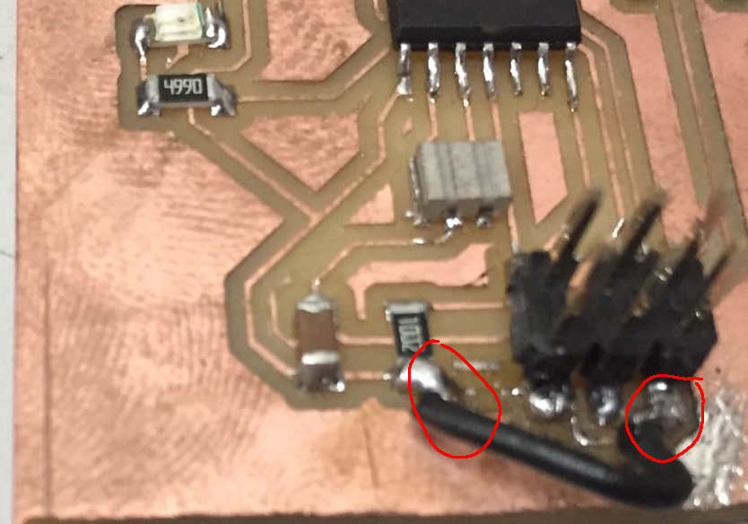 Traces cross soldered using a wire
 -
During the local review Francissco had expressed his concern in the strength of the soldered FTDI header in my PCB. To my bad luck it sheared off with the traces during the programming part :(. It seemed that I had to put holes in the PCB board during milling so as to keep the header fixed.
Sheared traces
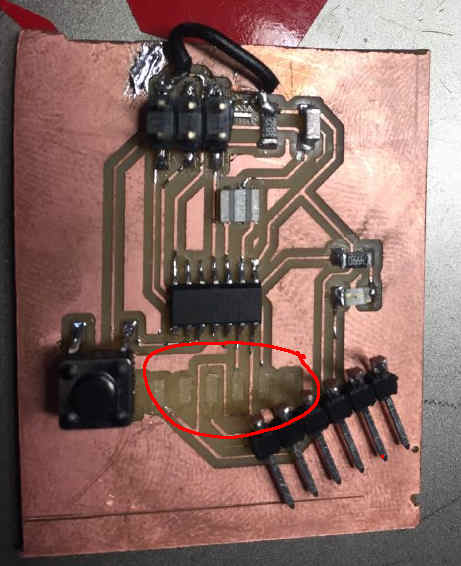
I am going to redesign the board fixing the above issues ! :)
 Redesigned Traces
 Finally ! fixed by providing flat header pins
files here
Programming the PCB
- Downloaded the programming files and make file from the archive.Copy the scripts onto a text editor and saved with
.cextension and.makeextension. - Renamed the make file as
Makefile. - Connect the PCB to the computer using ISP cable with the Incicuit programmer made in week 5.
- Open the terminal where the files are downloaded in step 1.
- Run the command
maketo make the hex file. - Run the command
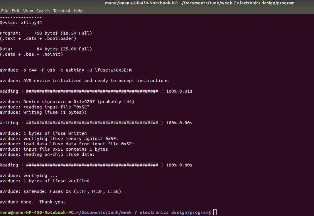
make program-usbtiny-fuses. - Finally
make program-usbtiny. - To check whether the PCB is programmed, a graphical serial terminal called
Cutecomwas downloaded and installed. - The PCB was connected to the computer using 6 pin FTDI cable to the computer.
- Cutecom was run to give instructions, the programme in the microcontroller caused to echo back the data given.
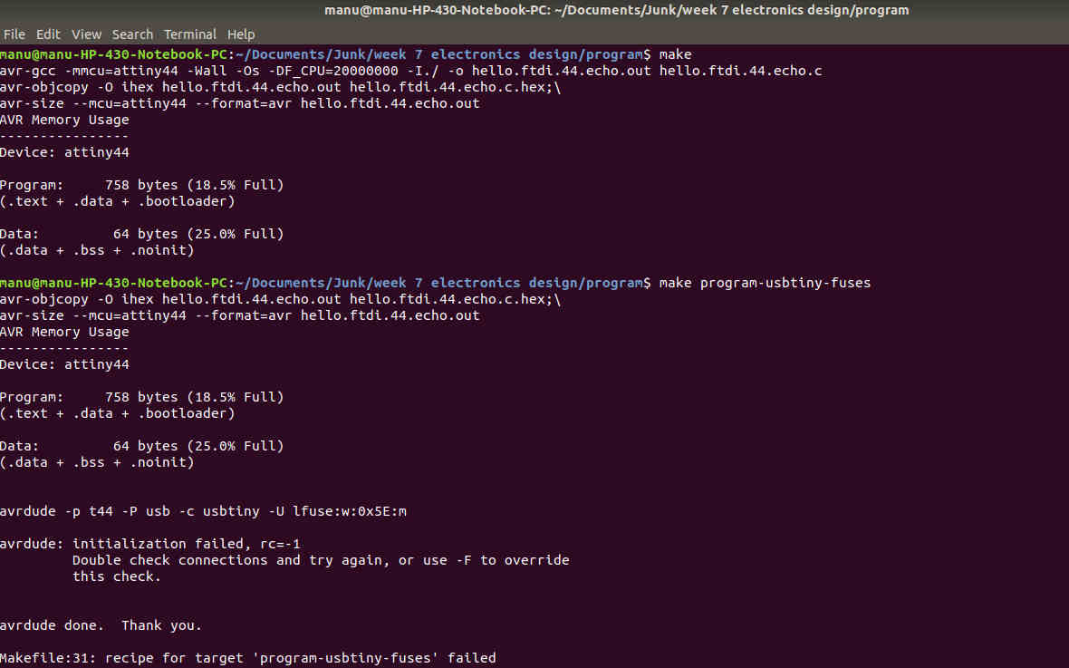 Error was there, it was found that ISP was connected wrongly.
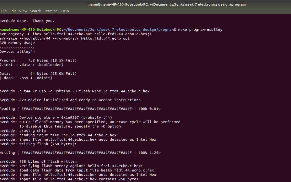 make program-usbtiny
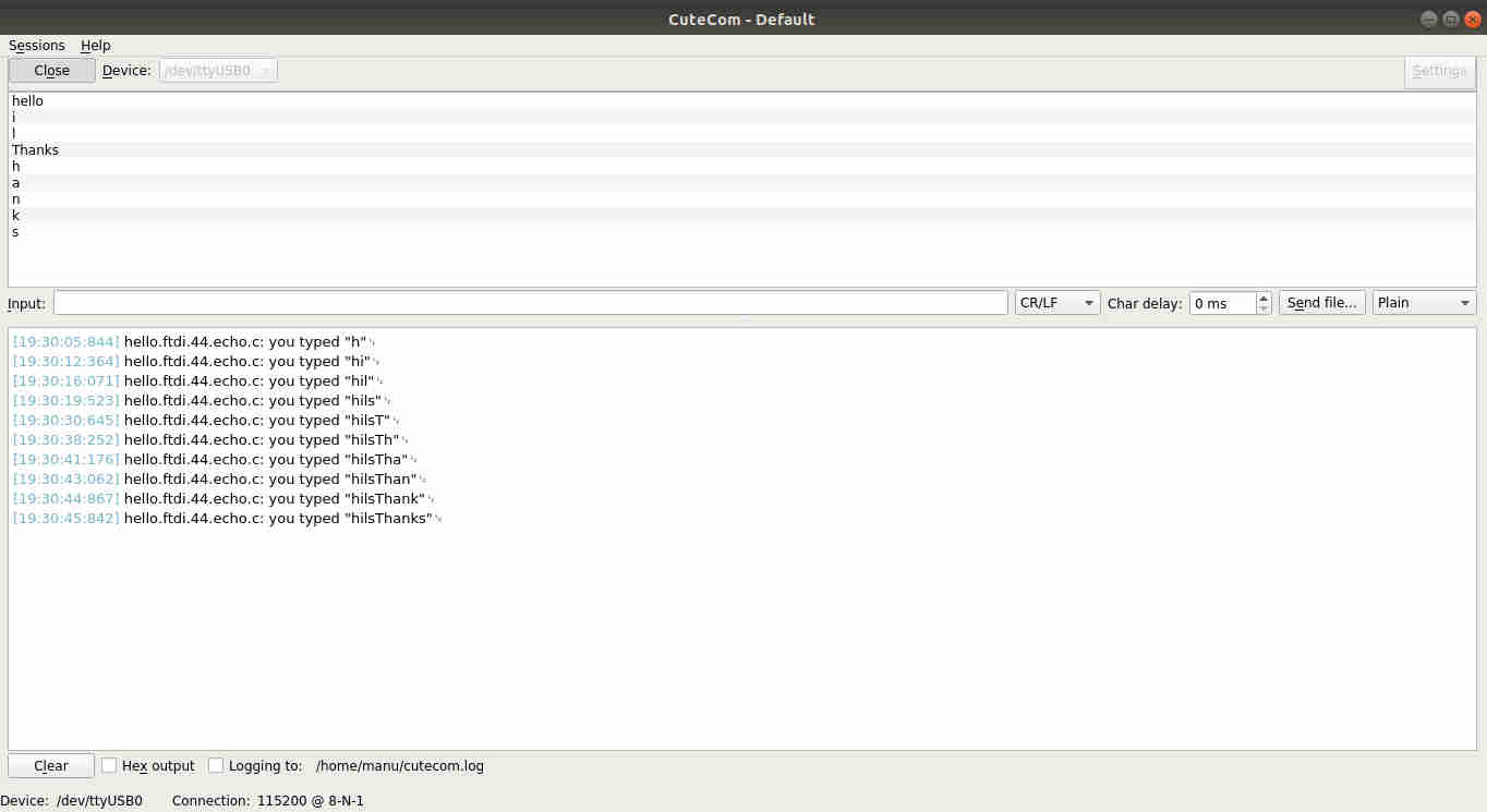
Here too the cutecom didn’t open first, only to realise that sudo privileges are required while opening Cutecom. (open Cutecom by typing sudo cutecom in the terminal).
I thank Suhail for his help in explaining the basics of program flashing and programming the Microcontroller.
Assignment-2 Group Assignment- To use the Test Equipment in the Electronics Lab
DigitalMultimeter
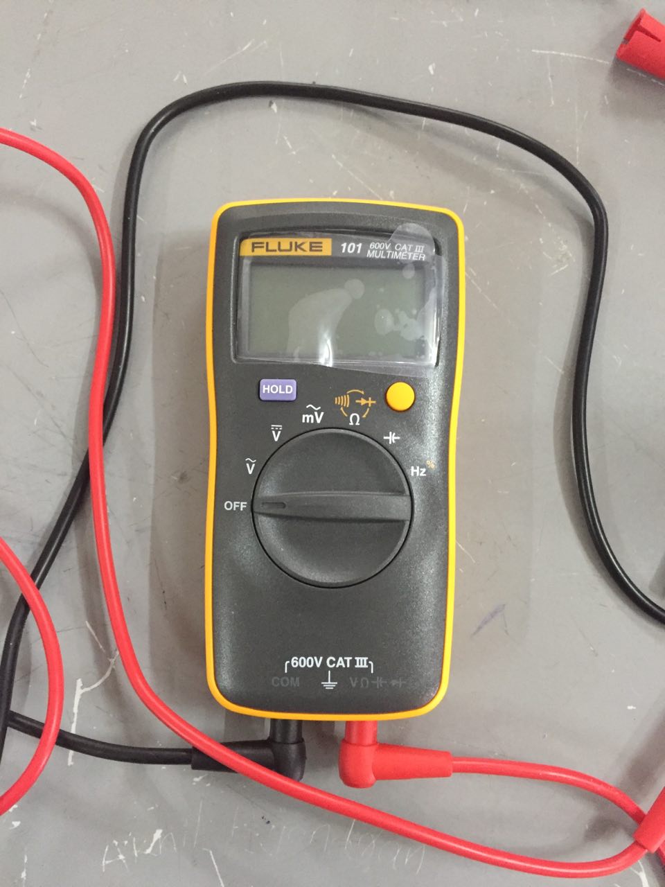 This is the multimeter used in the lab with which we check electrical continuity,resistance,capacitance,voltage,current etc. This had been my favourite and was used innumerable times through out my academy cycle. As seen in the picture it has two probes and the component to be tested would be used in between these two.
Regulated Power Supply
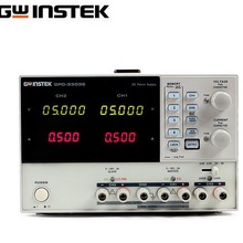
At times it becomes necessary that customised voltages and current are to be provided externally. In such cases a regulated power supply is used. This is the one used in the lab. It has two channels by which voltages can be given variably.
Oscilloscope
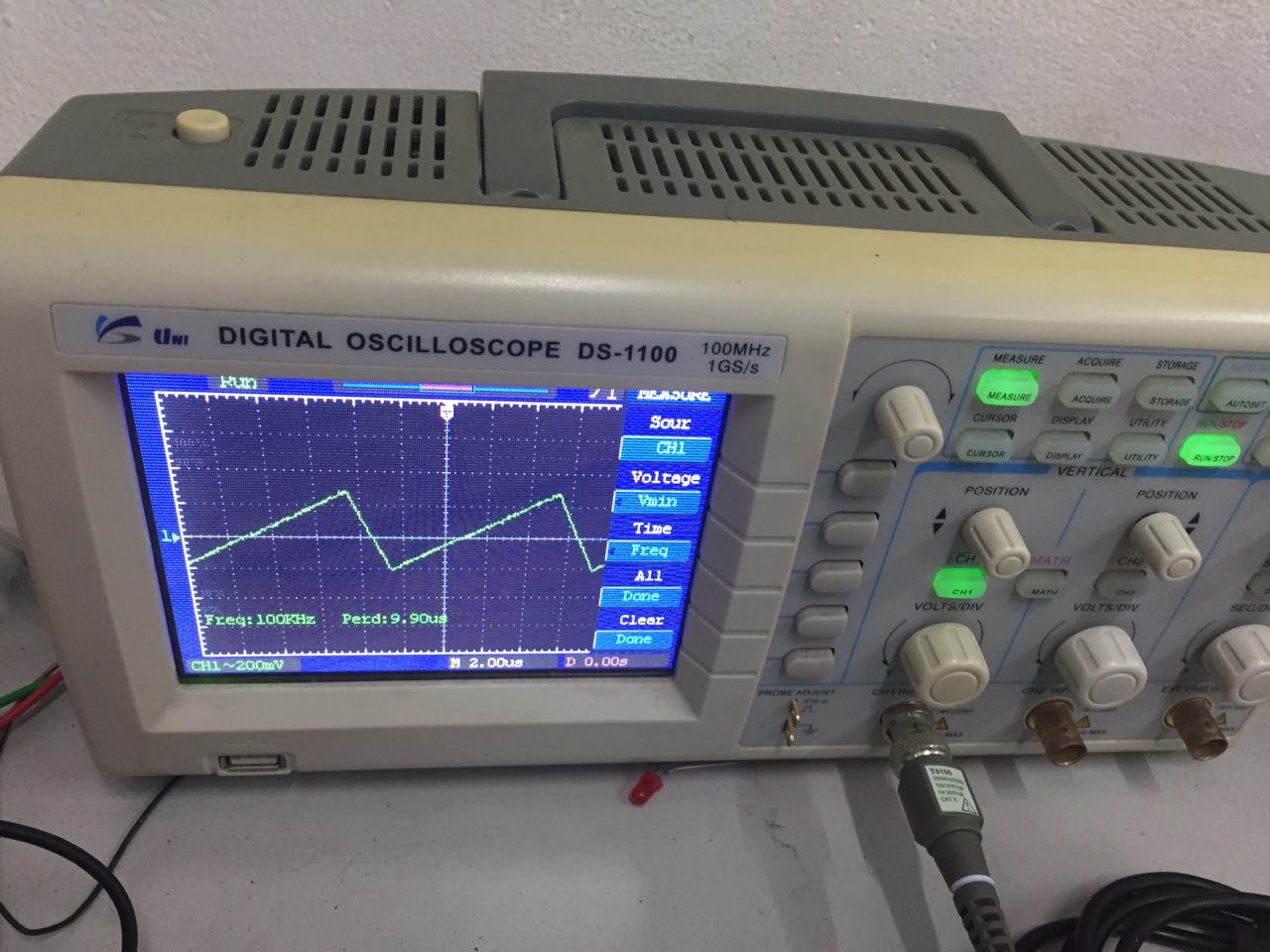 Oscilloscope is an instrument used to analyze signals in the circuit. Usually they give display in the form of 2D waveform. Details such as voltage, current,frequency etc can be viewed over a wide range of resolution, by adjustment.
Oscilloscope in the lab measuring a signal generated using a Function Generator instrument is seen in the figure above.
Oscilloscope is an instrument used to analyze signals in the circuit. Usually they give display in the form of 2D waveform. Details such as voltage, current,frequency etc can be viewed over a wide range of resolution, by adjustment.
Oscilloscope in the lab measuring a signal generated using a Function Generator instrument is seen in the figure above.
Testing the Microcontroller board
It was decided to test a board made in one of the week. The following code was flashed onto the MCU to generate a one second pulse. We will check the output of the MCU in the oscilloscope and check its coming alright. The board is powered externally using a regulated power supply instrument.
// This code is written for test purpose and it generates
// a pulse of 1 second duration.

void setup()
{

pinMode (A2,OUTPUT);// sets PA2 as output


}
void loop()
{


// Sets the PA2 pin for High state for 1000microseconds to generate the pulse

digitalWrite(A2, HIGH);
delayMicroseconds(1000);
digitalWrite(A2, LOW);
delayMicroseconds(1000);
}
Click to see the test video
In the video it’s seen that an external voltage of 4.8v is given at channel 2. The output obtained can be seen as pulse of 1 second duration in the Oscilloscope.