14. Networking and communications
After we had learnt of interfacing input devices and output devices with our MCU’s. Now its turn to make them to be able to communicate with each other. Say I have two or more multiple sensors with their MCU’s connected to a common master MCU,how would they communicate to each other. There are various networking protocols.
Serial and Parallel Communication
Electronic devices communicate each other through transferring bits of data between each other. Value of bit can be 1 or 0. Bits are transferred by quick changes in voltages between the devices. A 5v pulse will correspond to 1 and 0v pulse will be treated as 0. These bits can be transmitted either in Serial or Parallel form.In parallel communication, bits are all sent together simultaneously at the same time through seperate wires.
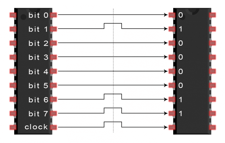 Here letter ‘C’(01000011 as binary) is sent parallely. The 8th bit is for the clock pulse data.
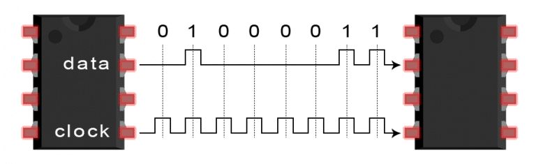 Here the data is sent serially through the data pin through a single wire
Image Courtesy:http://www.circuitbasics.com
Various forms of communciation protocols usually used are 1. Serial Periheral Interface (SPI) 2. Universal Asynchronous Receiver Transmitter (UART) 3. Inter Integrated Circuit (I2C)
Here I have selected I2C, the most versatile of the communciation protocols for testing. In all of these protocols the communicating devices have a master and slave relationship. One device will have the privelege of communciating with multiple nodes and send data to the slave nodes. Slave nodes would only be communicating back only to the chosen master node.
I2C
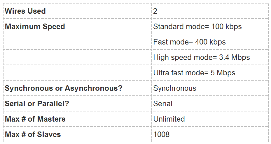
I2C or Tnter Integrated Circuit was found by Philips. It may also be referred as TWI or Two Wire Interface. It combines the best parts of both UART and SPI protocols. Like SPI a network can be made with multiple masters communicating to multiple slaves. Also it serially sends data and hence it needs only two wires.
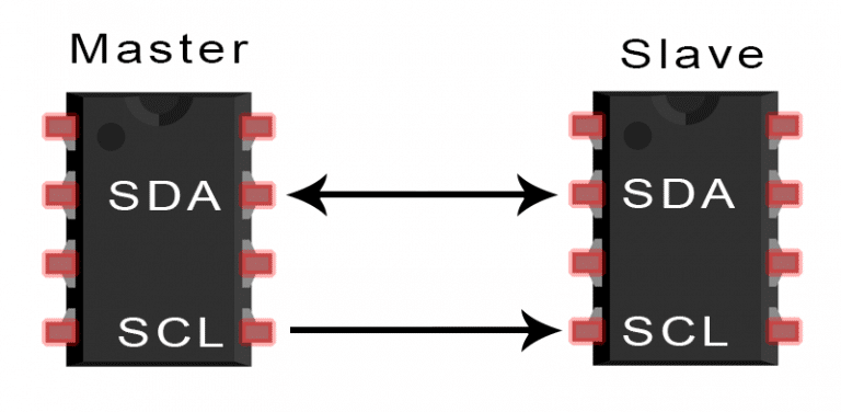 SDA (Serial Data) – The line for the master and slave to send and receive data.
SCL (Serial Clock) – The line that carries the clock signal.
Like SPI, I2C is synchronous, so the output of bits is synchronized to the sampling of bits by a clock signal shared between the master and the slave. The clock signal is always controlled by the master.
 Source:http://www.circuitbasics.com
With I2C, data is transferred in messages. Messages are broken up into frames of data. Each message has an address frame that contains the binary address of the slave, and one or more data frames that contain the data being transmitted. The message also includes start and stop conditions, read/write bits, and ACK/NACK bits between each data frame:
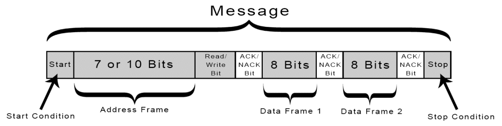
Start Condition: The SDA line switches from a high voltage level to a low voltage level before the SCL line switches from high to low.
Stop Condition: The SDA line switches from a low voltage level to a high voltage level after the SCL line switches from low to high.
Address Frame: A 7 or 10 bit sequence unique to each slave that identifies the slave when the master wants to talk to it.
Read/Write Bit: A single bit specifying whether the master is sending data to the slave (low voltage level) or requesting data from it (high voltage level).
ACK/NACK Bit: Each frame in a message is followed by an acknowledge/no-acknowledge bit. If an address frame or data frame was successfully received, an ACK bit is returned to the sender from the receiving device.
Steps in I2C communication
-
The master sends the start condition to every connected slave by switching the SDA line from a high voltage level to a low voltage level before switching the SCL line from high to low
-
The master sends each slave the 7 or 10 bit address of the slave it wants to communicate with, along with the read/write bit
-
Each slave compares the address sent from the master to its own address. If the address matches, the slave returns an ACK bit by pulling the SDA line low for one bit. If the address from the master does not match the slave’s own address, the slave leaves the SDA line high.
-
The master sends or receives the data frame.
-
After each data frame has been transferred, the receiving device returns another ACK bit to the sender to acknowledge successful receipt of the frame.
-
To stop the data transmission, the master sends a stop condition to the slave by switching SCL high before switching SDA high.
Source:http://www.circuitbasics.com
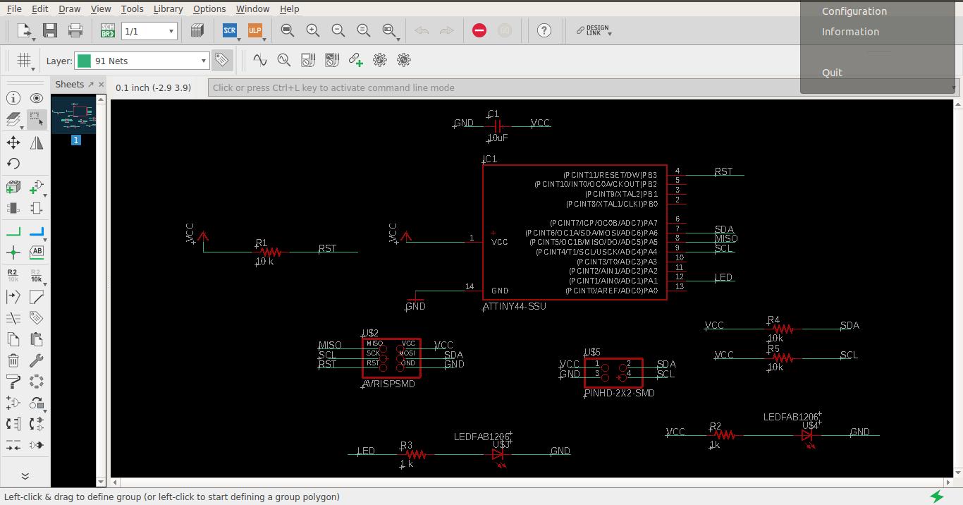
Designing the circuits- Trial 1
The circuits were designed using Eagle. Attiny 44 was used for both master and slave boards.The plan was that we will press switch in the master board to turn LED in the slave board on. Both SDA and SCL lines were pulled up using 10k ohm resistor. However some reading revealed that the ATtiny MCU’s are not supported for I2C protocol. TWI can be adopted through USI of these microcrontrollers. For that we need libraries called TinyWireM and TinyWireS. These were downloaded from Github.
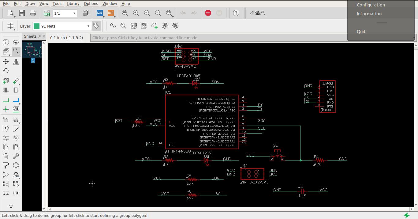 Master board
 Slave board
Eagle files here 
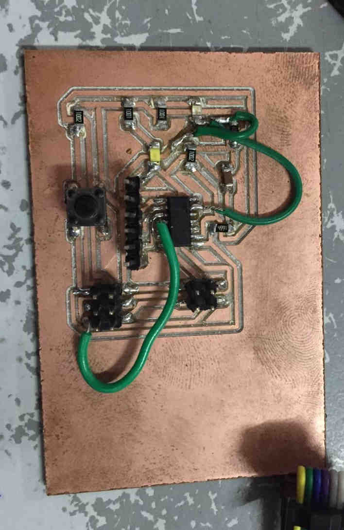 Master board after milling. In the schematic the LED was directly connected to the SDA line initially. Later it was changed to a dedicated pin PA0 and SDA lines are bypassed off the LED terminal. Also reset was accidently omitted. Hence airwires were provided and checked with a Multimeter for the continuity.
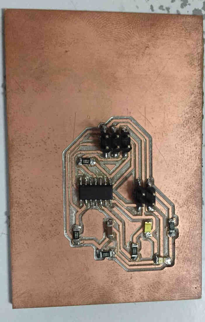 Slave board after milling
Programming the board-Trial 1
As usual the program was written using Arduino IDE.
This programm was written to control I2C slave.
The LED is connected to PA0 pin

#define I2C_SLAVE_ADDRESS 0x4 // Address of the slave

#include <TinyWireS.h> // Include TinyWireSlave Library

int i=0;

void setup()
{
    TinyWireS.begin(I2C_SLAVE_ADDRESS); // join i2c network
    //TinyWireS.onReceive(receiveEvent); // not using this
    TinyWireS.onRequest(requestEvent);

    // Turn on LED when program starts
    pinMode(0, OUTPUT);
    digitalWrite(0, HIGH);
}

void loop()
{
    // This needs to be here
    TinyWireS_stop_check();
}

// Gets called when the ATtiny receives an i2c request
void requestEvent()
{
    TinyWireS.send(i);
    i++;
}
Program for I2C master
This programm was written to control I2C master.

#include <TinyWireM.h> // Including I2C master library for ATtiny

                          series master
#define slave (0x4)
#define BTN 5
#define LED 0

void setup() {
pinMode(BTN,INPUT);
pinMode(LED,OUTPUT);
TinyWireM.begin();

}
void loop() {
TinyWireM.beginTransmission(slave);

int val = analogRead(BTN);
if(BTN>0)
{

TinyWireM.beginTransmission(slave);
digitalWrite(LED,HIGH);
TinyWireM.send(1);
TinyWireM.endTransmission();

}
else
{TinyWireM.beginTransmission(slave);
digitalWrite(LED,LOW);
TinyWireM.send(0);
TinyWireM.endTransmission();
}
}
Out of badluck it didn’t work. I checked for various possibilities of short circuits, break in continuity, but nothing helped me. The problem could have been with the installed libraries. The issue that was haunting me was that I was really running out of time. I decided that I shall use two MCU’s with Atmel328p chips. To test it I had to manufacture atleast a board with 328p. The reason was that it had the dedicated SDA and SCL pins for I2C communication.
Designing the circuits- Trial 2 (with 328p)
First trial was to network and use a board with Atmel328p as master and the previous slave boards.
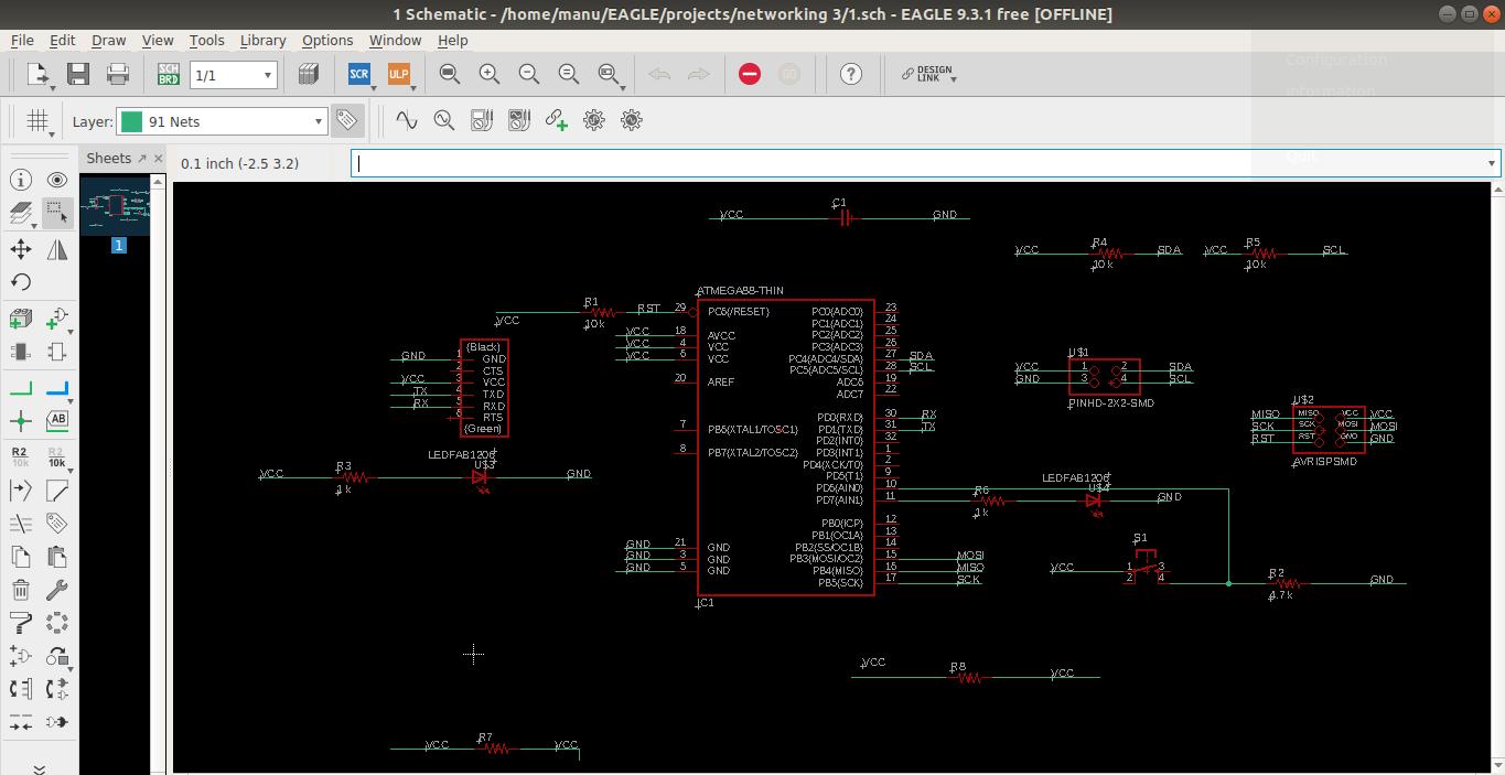 Schematic of the master board
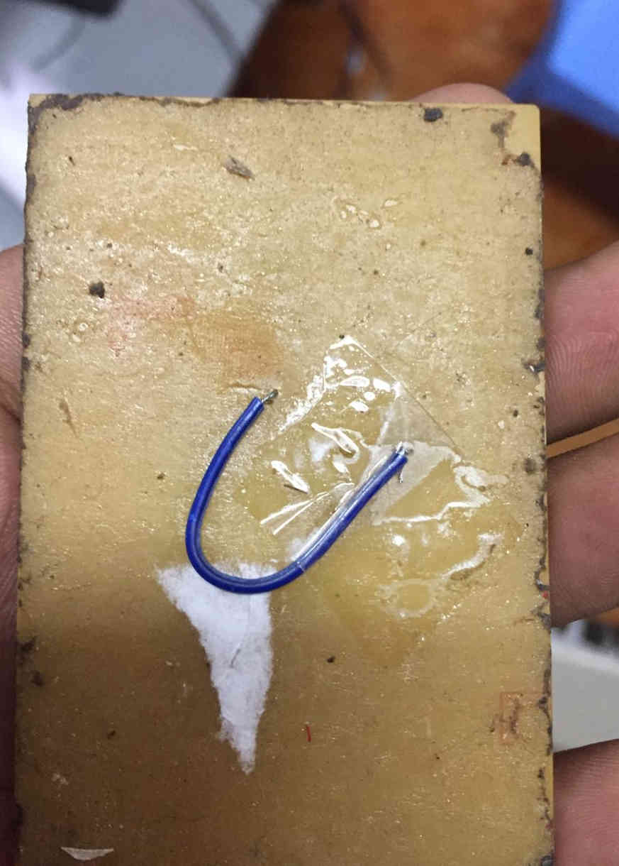
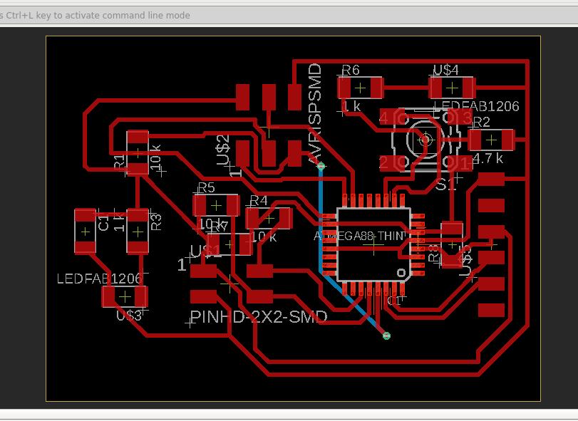 Blue wire as airwires
Master Board Design Files here
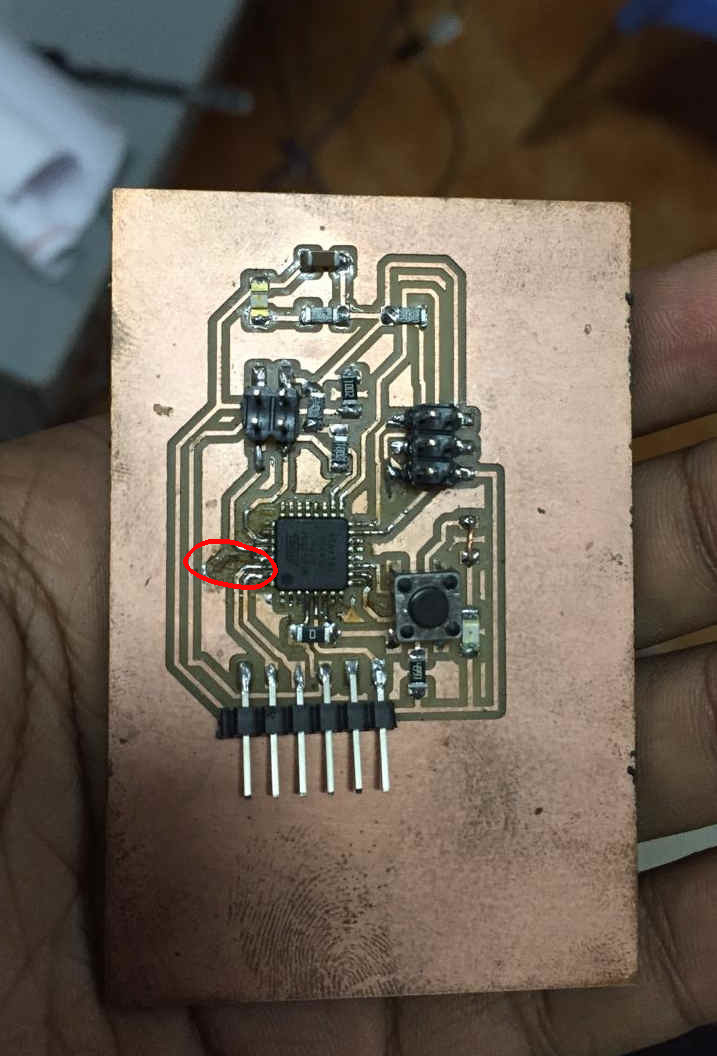 Milled board. Peeled off trace in red circle.
Errors
- Soldering 328p in the board posed the main challenge. Pins are so small and it really tested my patience and time. Unfortunately the board didn’t work. I found that at one pin connection the trace just peeled off from the board. To fix that a hole was drilled beside the pin and a through hole was made to connect the trace as shown below.
- I just found that still my board is not functioning. I wasn’t able to flash the program on to it. It was speculated that sometimes I would have accidently flashed bootloader with a wrong internal/external frequency. To check that we connected a seperate outside SMD Resonator of 20MHz and connected it near the MCU. Out of surprise it worked and we were able to reprogram the board and tell its internal clock is with 8 MHz. It was a nice experience on how much things can go wrong with circuits !
I really thank my instructor Yedu for patiently helping me out with this.
The connections were checked with Multimeter for short circuits and continuity. Its all good.
Programming the Board Trial-2
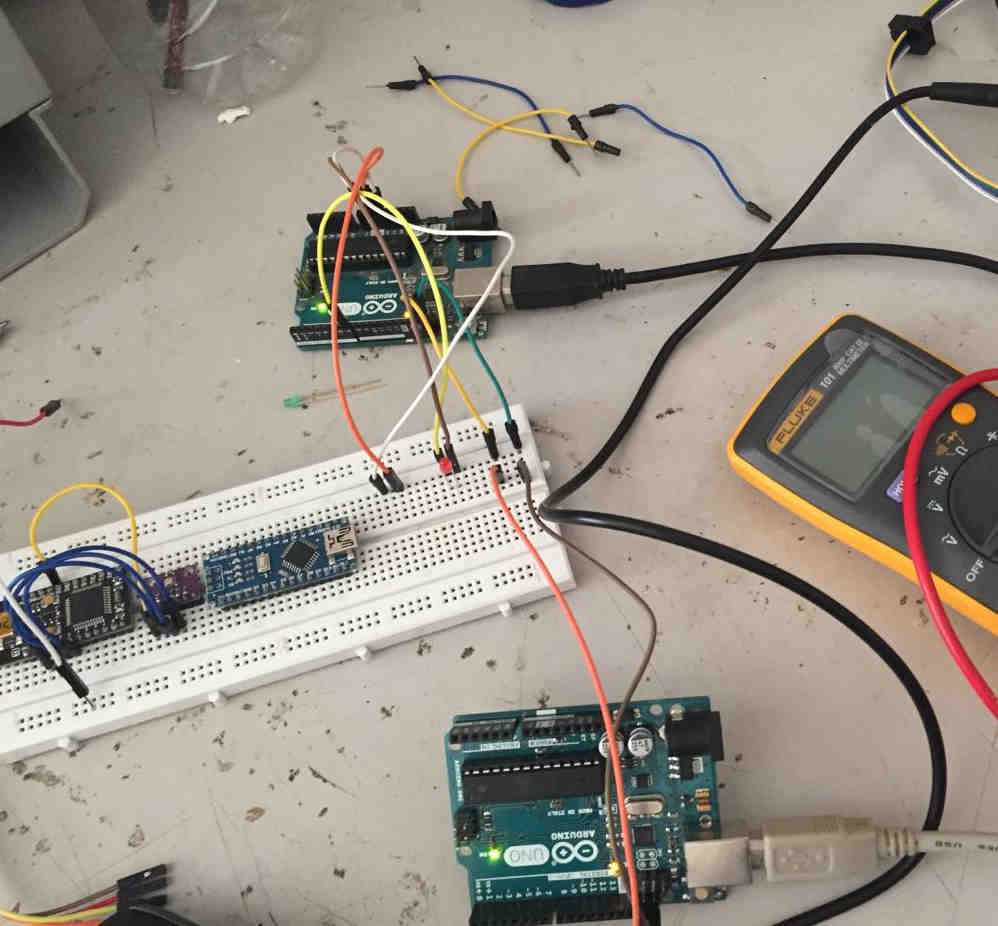
This time, out of caution I decided that I will try a new program and test it with two arduino uno’s and then use the real board. This program was available and I modified and used it for my use.
// This is a program for the master UNO board to send a variable 'x' to the desired slave with address '8'.It is referred from the program below
// Wire Master Writer
// by Nicholas Zambetti < http://www.zambetti.com>

// Demonstrates use of the Wire library
// Writes data to an I2C/TWI slave device
// Refer to the "Wire Slave Receiver" example for use with this

// Created 29 March 2006

// This example code is in the public domain.


#include <Wire.h>

void setup() {
  Wire.begin(); // join i2c bus (address optional for master)
}

byte x = 0;

void loop() {
  Wire.beginTransmission(4); // transmit to device 4
//  Wire.write("x is ");        // sends five bytes
//  Wire.write(x);              // sends one byte
  Wire.write(x);
  Wire.endTransmission();    // stop transmitting

  x++;
  delay(500);
}
Master Board program
// This is a program for the slave UNO board to receive variable 'x' and use the modulus operator to flash the LED's connected at digital pin 7.
//  It is referred from the program below
// Wire Slave Receiver
// by Nicholas Zambetti < http://www.zambetti.com>

// Demonstrates use of the Wire library
// Receives data as an I2C/TWI slave device
// Refer to the "Wire Master Writer" example for use with this

// Created 29 March 2006

// This example code is in the public domain.


#include <Wire.h>

void setup() {
  Wire.begin(4);                // join i2c bus with address 4
  Wire.onReceive(receiveEvent); // register event
  Serial.begin(9600);           // start serial for output
}

void loop() {
  delay(100);
}

// function that executes whenever data is received from master
// this function is registered as an event, see setup()
void receiveEvent(int howMany) {
//  while (1 < Wire.available()) { // loop through all but the last
//    char c = Wire.read(); // receive byte as a character
//    Serial.print(c);         // print the character
//  }
  int x = Wire.read();    // receive byte as an integer
//  Serial.println(x);         // print the integer
//  Serial.println(x%5);
  if (x%5 == 0)
  {
    digitalWrite(7, HIGH);
  }
  else
  {
    digitalWrite(7, LOW);
  }
}
Slave Board Program
I found that its working. The LED was blinking. So the program is working.
Arduino UNO Working Video
I flashed this to my board and found that it’s working. Though I didn’t take video of it, I decided that I will interface it with the Amal’s Output Week board. It too had Atmel328p MCU. But the issue was that it didn’t had LED to show. So I made it master and my board as slave. I flashed the above program and found that its working.
Final master and Slave Working Video
The blinking of LED is feeble. I am working to find the reason. Initially I thought it was because of the 1k ohm resistor connected across it.Then I changed and soldered with 499 ohm, but of no use.I am yet to figure it out.
Overall this has been the toughest week, but I am happy that I was able to network two boards and send information through I2C channel.
Video of the serial output of the slave
The above video shows the serial output of the slave board (with blinking LED) in Aurduino IDE. In the computer monitor we can see the numbers getting printed incrementally(upto 255). The master is programed to generated integers sequentially using x++ and that number is being sent to the slave board referred with address 4. The received number is being operated by a modulus operand x%5 to check the logic for turning the LED on/off in the slave board. The integers printed in the serial monitor is the proof that the slave board is receiving the integers generated by the master board. In the video the FTDI conenctor is connector with so many jumper wires as the pins for RX and TX got interchanged in the slave board. This is fixed by connecting with jumper wires in right fashion. (Rather than changing the circuit in the board). Also previously the blinking of the LED is feeble, this has been fixed by adding a line of defining the output pin no. 7 with the command line pinMode(7,OUTPUT). The updated programe codes for the master and the slave is attached below.