9. Embedded programming
Group Assignment
1. Harvard architecture
The Harvard architecture is a computer architecture with physically separate storage and signal pathways for instructions and data. The term originated from the Harvard Mark I relay-based computer, which stored instructions on punched tape (24 bits wide) and data in electro-mechanical counters. These early machines had data storage entirely contained within the central processing unit, and provided no access to the instruction storage as data. Programs needed to be loaded by an operator; the processor could not initialize itself. Today, most processors implement such separate signal pathways for performance reasons, but actually implement a modified Harvard architecture, so they can support tasks like loading a program from disk storage as data and then executing it.
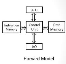
A. Memory In a Harvard architecture, there is no need to make the two memories share characteristics. In particular, the word width, timing, implementation technology, and memory address structure can differ. In some systems, instructions for pre-programmed tasks can be stored in read-only memory while data memory generally requires read-write memory. In some systems, there is much more instruction memory than data memory so instruction addresses are wider than data addresses.
B. Applications and features of Harvard Architectures The principal advantage of the pure Harvard architecture—simultaneous access to more than one memory system—has been reduced by modified Harvard processors using modern CPU cache systems. Relatively pure Harvard architecture machines are used mostly in applications where trade-offs, like the cost and power savings from omitting caches, outweigh the programming penalties from featuring distinct code and data address spaces. Digital signal processors (DSPs) generally execute small, highly optimized audio or video processing algorithms. They avoid caches because their behavior must be extremely reproducible. The difficulties of coping with multiple address spaces are of secondary concern to speed of execution. Consequently, some DSPs feature multiple data memories in distinct address spaces to facilitate SIMD and VLIW processing. Texas Instruments TMS320 C55x processors, for one example, feature multiple parallel data buses (two write, three read) and one instruction bus. Microcontrollers are characterized by having small amounts of program (flash memory) and data (SRAM) memory, and take advantage of the Harvard architecture to speed processing by concurrent instruction and data access. The separate storage means the program and data memories may feature different bit widths, for example using 16-bit wide instructions and 8-bit wide data. They also mean that instruction prefetch can be performed in parallel with other activities. Examples include the PIC by Microchip Technology, Inc. and the AVR by Atmel Corp (now part of Microchip Technology).
C. The speed aspect A lot has been discussed about the Harvard architecture, but without the speed any architecture can’t be accepted. But in case of the Havard architecture the manufacturers have designed the architecture in such a way that it will be able to process the data with a much higher speed. Yes, all care has been taken so that the architecture can process data with a high speed.By implementing the same formula the modern days CPU are being manufactured so that the new CPU can run with a much faster sped and can also process the data effectively. The concept of the CPU cache is also being implemented while designing the Harvard architecture.
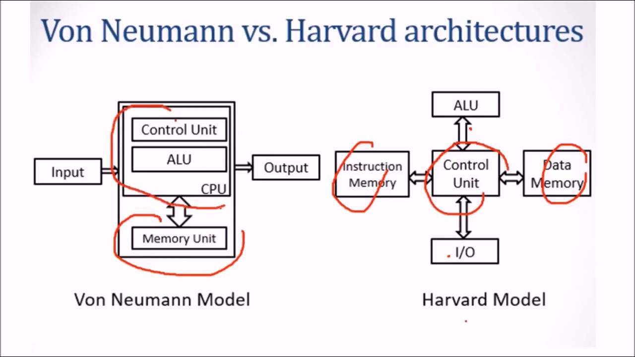
2. Von Neumann Architecture
The von Neumann architecture, which is also known as the von Neumann model and Princeton architecture, is a computer architecture based on the 1945 description by the mathematician and physicist John von Neumann and others in the First Draft of a Report on the EDVAC. This describes a design architecture for an electronic digital computer with parts consisting of a processing unit containing an arithmetic logic unit and processor registers; a control unit containing an instruction register and program counter; a memory to store both data and instructions; external mass storage; and input and output mechanisms. The meaning has evolved to be any stored-program computer in which an instruction fetch and a data operation cannot occur at the same time because they share a common bus. This is referred to as the von Neumann bottleneck and often limits the performance of the system.
The design of a von Neumann architecture machine is simpler than that of a Harvard architecture machine, which is also a stored-program system but has one dedicated set of address and data buses for reading data from and writing data to memory, and another set of address and data buses for instruction fetching.
 A.Applications and features of Von Neumann Architecture
The Von Neuman architecture has got extensive application in everyday life. Keeping in mind the extensive application the Von Neuman architecture has been introduced as a subject in the engendering degree. From the third semester engineering students will have the subject as their curriculum. The Von Neuman architecture consists of some important features and here we will have a detailed elaboration to the features.
A.Applications and features of Von Neumann Architecture
The Von Neuman architecture has got extensive application in everyday life. Keeping in mind the extensive application the Von Neuman architecture has been introduced as a subject in the engendering degree. From the third semester engineering students will have the subject as their curriculum. The Von Neuman architecture consists of some important features and here we will have a detailed elaboration to the features.
B. Memory: We all know that the Von Neuman is nothing but a computer having the feature of data storage. In the architecture of the Von Neuman the memory plays a vital role and it is considered as one of the important feature. Mainly this is responsible for both holding and starting of data and programming data. In modern days this has been replaced by the RAM and now we are using RAM for this purpose.
C. Control Unit: This unit is mainly responsible for the controlling aspect. All the data stored in the memory and during the processing of data the control unit plays the role and it manages the data flow. In fact, to be more typically it is “One At A Time”. The control unit follows the principle of the One At A Time and accordingly it process all the data.
D. Input– output: Like all electronics devices the Von Neuman architecture also has an input/output architecture. It is the basic function is same and nothing specially has been designed for the input and output architecture. With the Input and output device on a person can communicate with the device.
E. ALU: ALU or the Arithmetic Logic Unit has a great importance in the Von Neuman architecture. Any sort of addition, subtraction, multiplication and division of the data will be carried out by this ALU. In addition to that any other kind of algorithmic function and activities will be carried out by the ALU. These are the basic aspect of the Von Neuman architecture which you must aware of.
Difference between Harvard and Von Neumann Architecture
A. Harvard Arhitecture
a. The name is originated from “Harvard Mark I” a relay based old computer.
b. It required two memories for their instruction and data.
c. Design of Harvard architecture is complicated.
d. Harvard architecture is required separate bus for instruction and data.
e. Processor can complete an instruction in one cycle
f. Easier to pipeline, so high performance can be achieve.
g. Comparatively high cost.
B. Von Neumann Architecture
a. It is named after the mathematician and early computer scientist John Von Neumann.
b. It required only one memory for their instruction and data.
c. Design of the von Neumann architecture is simple.
d. Von Neumann architecture is required only one bus for instruction and data.
e. Processor needs two clock cycles to complete an instruction.
f. Low performance as compared to Harvard architecture.
g. It is cheaper.
Raspberry Pi
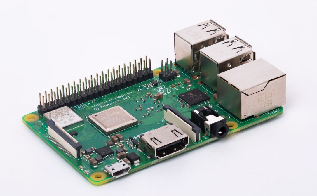
As part of the group assignment we all understood the basics of Raspberry Pi and programmed it.Raspberry Pi is a general-purpose computer, usually with a Linux operating system, and the ability to run multiple programs.
a. CHIP- Broadcom BCM2835 SoC
b. Core Architecture- ARM11
c. CPU- 700 MHz Low Power ARM1176JZFS
d. GPU- Dual Core VideoCore IV® Multimedia Co-Processor
e. Memory- 512MB SDRAM
f. Operating system- Boots from Micro SD card, running a version of the Linux operating system
g. Dimension- 85 x 56 x 17mm
h. Power- Micro USB socket 5V, 2A
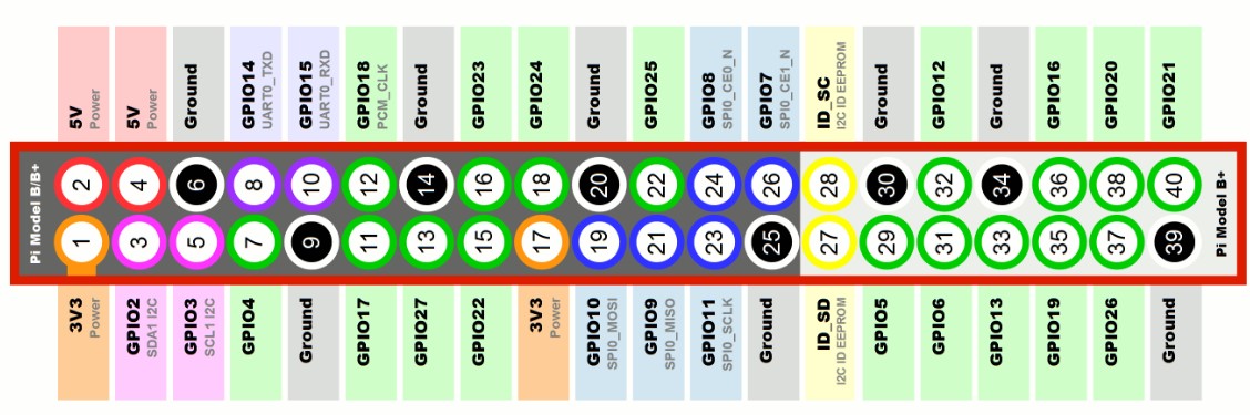
We referred the below pin out diagram for programming LED to blink:
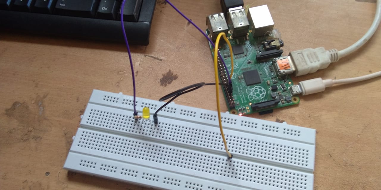
The picture below shows the setup and circuit connection:
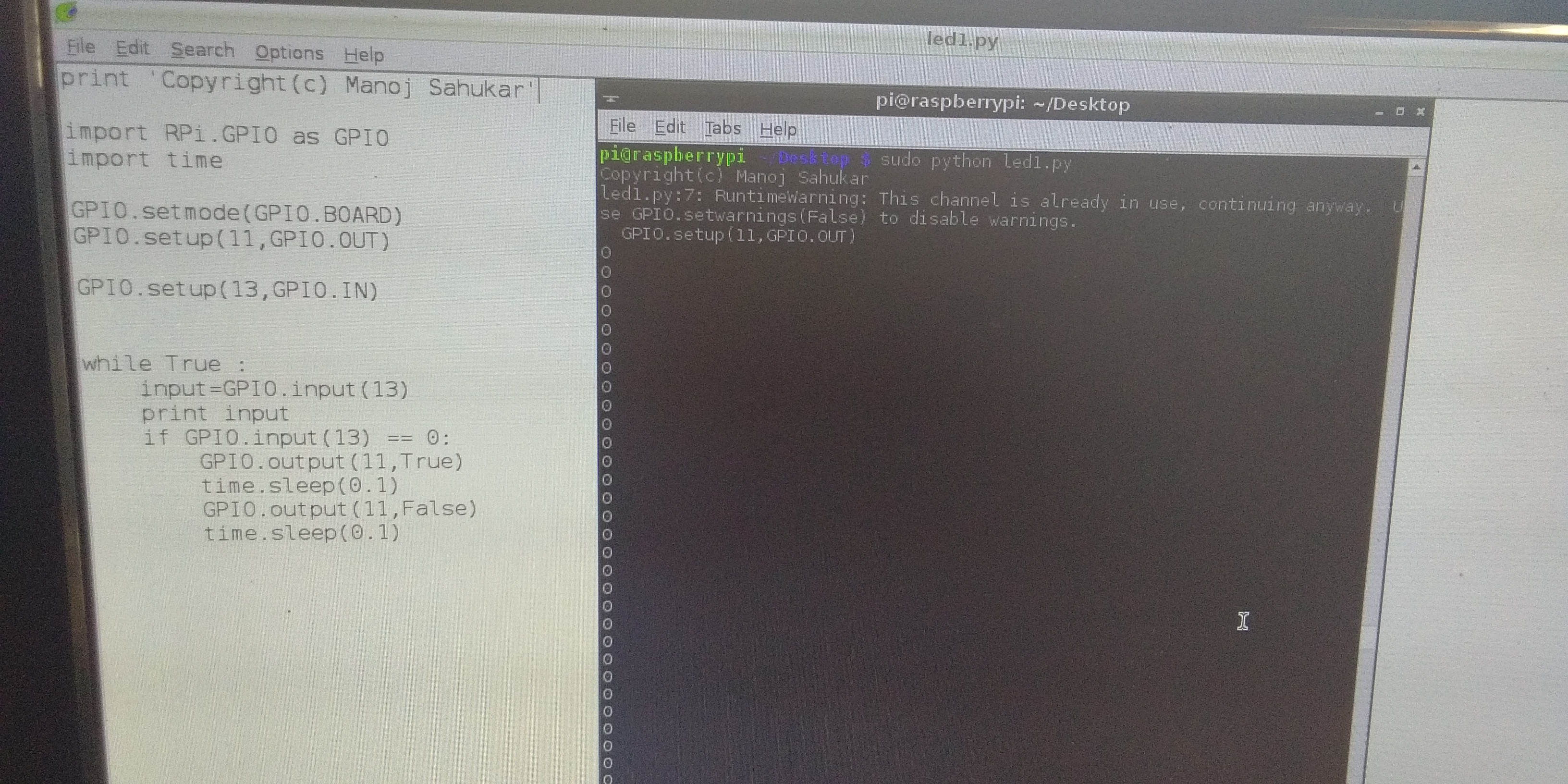
After loading the programme we got the LED blinking.
Comparison between “Arduino” and “Raspberry Pi” architectures:
a. Arduino has 0.002MB & Raspberry Pi has 512 MB memory.Clearly Raspberry Pi should be used for higher end applications.
b. Raspberry Pi is a fully functional computer while Arduino is a just microcontroller.
c. Arduino has 16 Mhz clock cycle and for Raspberry Pi it is 700Mhz.
d. Raspberry Pi has wired ethernet network on the other hand arduino doesnot have any network.
e. Arduino has 1 USB input whereas Rasperry Pi has 2.
f. Costwise there is no much difference.
Individual Assignment
Understanding ATMEL Datasheet:
I went through the Atmel Datasheet. The document is very big and not easy to understand. I skimmed through the topics and learnt the following:
1. The ATTiny44 is high Performance, low Power 8-bit Microcontroller with advanced RISC architecture. These are its general features:
a. 4K Bytes of Flash Program Memory
b. 256 Bytes of Programmable EEPROM
c. 256 bytes SRAM
9
d. 12 general purpose I/O lines
e. 32 general purpose working registers and 8-channel 10-bit ADC.
f. Internal calibrated oscillator
g. Operating voltage supply between 1.8 ~ 5.5V.
2. There are two kinds of ports:
a. Port A pins are 8-bit bi-directional I/O port with internal pull-up resistors (pin names are from PA0 to PA7)
b. Port B pins are 4-bit bi-directional I/O port with internal pull-up resistors (pin names are from PB0 to PB3).
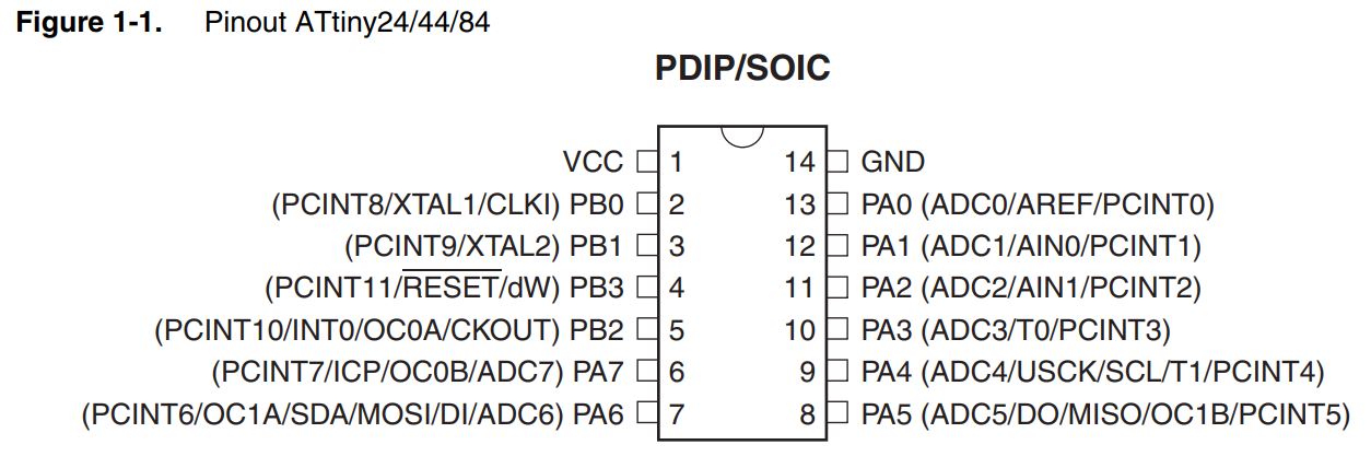
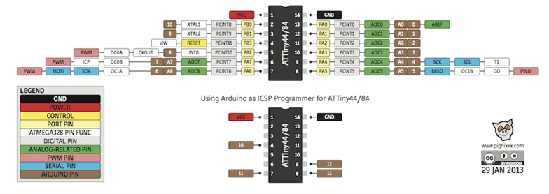
3.Pin layout of ATtiny 44:
4.Memory and Clocks:
1. The CPU core runs on the AVR architecture.
2. The ATtiny24/44/84 chips have three different types of memory:
a. Data Memory (Static and Dynamic RAM). SRAM memory is used for storing your data which is processed during the run time (including also the registers) - volatile memory
b. The Program Memory is a reprogrammable flash memory that stores the program - non volatile. It can endure up to 10,000 write/erase cycles.
c. EEPROM memory can be used for storing non volatile data and changeable during run-time. (for example: setting values) Endurance: 100,000 Write/Erase Cycles.
3. The chip contains four different clocks CPU Clock, I/O Clock, Flash Clock, and ADC Clock.The internal oscillator is the default clock and it runs at 8mHz.
Programmed my “Hello World Board” using USBtinyISP in Arduino:
1.Installed ATtiny support
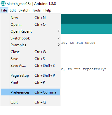
A. Prefernces: File>Prefernces.Opened the preferences dialog in the Arduino software.
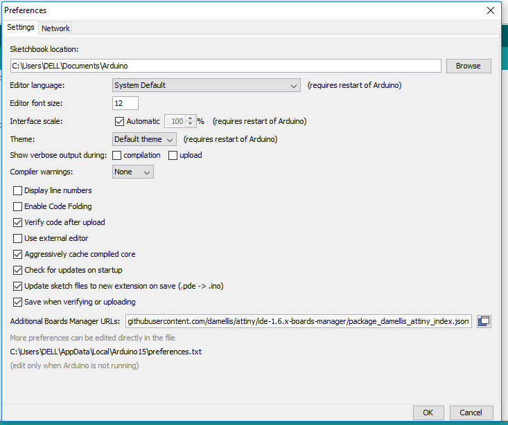
B. Added Board:The bottom of the dialog has the “Additional Boards Manager URLs” field.Added the URL into the field (https://raw.githubusercontent.com/damellis/attiny/ide-1.6.x-boards-manager/package_damellis_attiny_index.json)
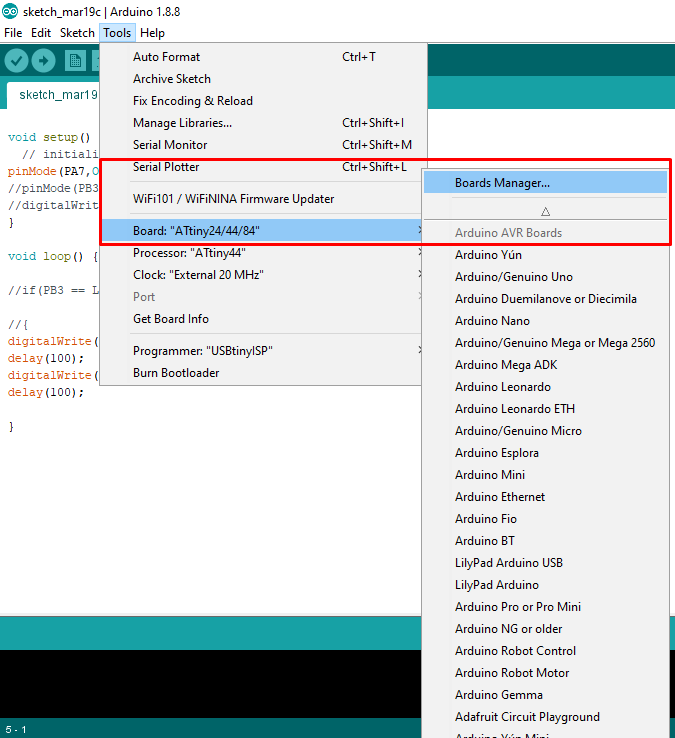
C. Board Manager: Tools>Board. The board manager basically shows the list of the boards which can be installed.
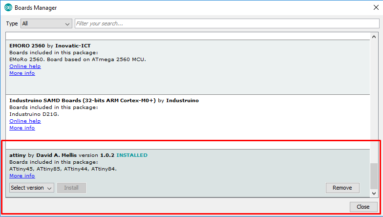
D. Installed ATtiny Boards: ATtiny44,ATtiny84,ATtiny85,ATtiny45 boards were added.
2. Programming:
I. Ardunio Blink Code:
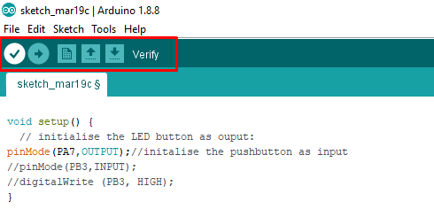
A. Code: I wrote a programme for LED in “Hello World” board to blink. Added command to give PA7 output which has LED attached.
//
Created by Tushar Kukreja
Date: March 2019
//

int buttonstate=HIGH;     //variable for reading pushbutton status

void setup() {
  // initialise the LED button as ouput:
pinMode(PA7,OUTPUT);//initalise the pushbutton as input
pinMode(PA0,INPUT);
}

void loop() {
  // read the state of pushbutton value:
//buttonStat = digitalRead(PA0); // Read the state of pushbutton. If the pushbutton value is HIGH:
if(PA0, HIGH)// turn LED on
digitalWrite(PA7, HIGH);
else
 //turn LED off:
   digitalWrite(PA7, LOW);
 }
B.Code Explaination:
i. Setup ( ) is the preparation block and loop ( ) is an execution block.
ii. The setup function is the first to execute when the program is executed, and this function is called only once. The setup function is used to initialize the pin modes and start serial communication.
iii. loop ( ) function is a part of execution block.The loop( ) function executes the set of statements repeatedly. So, it will blink LED if the state ofpushbutton is high.
C.Verify: The errors were corrected and the programme was made error proof.Ready to be uploaded on the board.
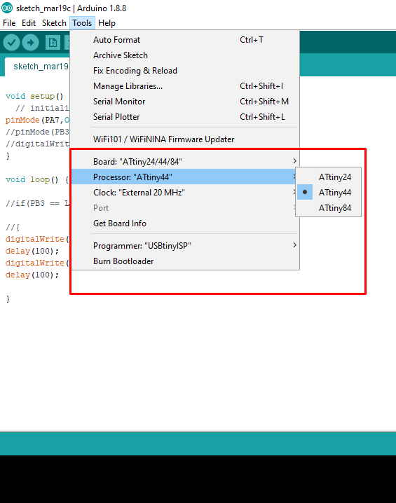
D. Tools: Selected the following commands
a. Board: ATtiny 24/44/84
b. Processor: ATtiny 44
c. Clock: External 20Mhz
d. Programmer: USBtinyISP
E.Bootloader: bootloader is a section of program memory that runs before the main code runs.
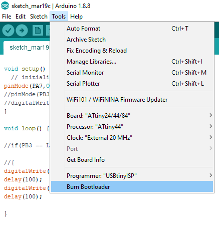
F. uploading and Output:
programme uploaded successfully and LED blinked
II. C Code for Blink: 
A. Code in C language:
//
Written by Tushar Kukreja
Date: September 2019
//
#define F_CPU 20000000  //Define clcok speed as 1Mhz
#include<avr/io.h>     //Import header file required for AVR microcontrollers
#include<util/delay.h>   //Import header flie required for delay function
int main(void)
{
  DDRA = 0b00000010;  //set PA3as output & all other pins as input
    while (1) //Repeat the below actions continuously
    {
    PORTA |= (1<<3);// Set PA7 high (Make LED ON)
    _delay_ms(1000);//delay of 1 sec
    PORTA &= ~(1<<3);// Set PA7 low (Make LED OFF)
    _delay_ms(1000);//delay of 1 sec
  }
}
B. Code Explaination:
i. CPU is frequency in Hz.Here, the clock speed is defined as 1Mhz.It is simply informing the library code how many CPU cycles per second the processor is executing.
ii. The code needs 2 libraries to be included AVR microcontrollers and Delay function.
iii. Data Direction Register(DDR) decides whether the pins of a port are input pins or output pins. If the pin is input, then the voltage at that pin is undecided until an external voltage is applied. PA3 pin has been set as output and rest all the pins input.
iv. & is bitwise AND,~ is bitwise NOT and | is bitwise OR. Also, a delay of 1 sec has been assigned.
C.Uploading Code and Output:
Terms and Definitions:
1.EEPROM:Electrically Erasable Programmable Read-Only Memory.
2.SRAM (static RAM): is random access memory (RAM) that retains data bits in its memory as long as power is being supplied.
3. ADC: Analog to Digital Converter
4. Differnce between 8 and 16 bit microcontroller:
a. 16 bit microcontrollers have twice as long data pipe than the 8 bit microcontroller
b. 16 bit microcontrollers are more accurate at math than
c. 16 bit microcontrollers are more efficient than 8 bit microcontrollers in math operation greater than 8 bits
d. 16 bit microcontrollers have longer timers than 8 bit microcontrollers
e. 16 bit microcontrollers are slightly more expensive than 8 bit microcontrollers
5. ISP:0 In-system programming,is the ability of some programmable logic devices, microcontrollers, and other embedded devices to be programmed while installed in a complete system, rather than requiring the chip to be programmed prior to installing it into the system.