Week 7. Electronics Design
7. Electronics design

Assignment
Group assignment: “Characterize the design rules for your PCB production process” Individual assignment: “Make an in-circuit programmer by milling the PCB, program it, then optionally, trying other processes.”
Software
KiCad, open source electronics design tool suite.
Mods, control software for the Roland mill
Hardware
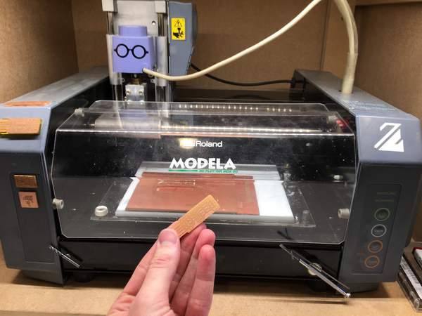
Roland Modella MDX-20 mill
with the mill bit for traces - mini end mills two flutes 0.40 mm 826 (damen.cc)
with the mill bit for cutout - two flutes 0.8 mm
Multimeter
Knife
Anti static tweezers for electrical components
Solder iron
Solder tin
Various surface mounted components
A regulated digital controlled DC power supply
An oscilloscope
Files
Trace lines file
Cutout file for holes
Cutout file
KiCad design files
Electronics 101

We will be creating electronic boards. For this is it is good to know your electronics basics.
Here are some helpful links:
- Neil’s lesson with links to different software and important keywords
- Learn about Power, Current, Voltage, Resistance and how to calculate with them
- Learn about electronic components
Before you start
- No long hair, sleeves etc. When soldering you can turn this on fire and when milling it can get stuck in the mill.
- Do not be static, you are working with sensitive electronics, static electricity can break it. Remove your static by touching a grounded metal, like a radiator or wear anti-static arm band.
- Provide good ventilation and work clean. You are working with potentially toxic material.
- Wash your hands after you finished your work.
From scheme to a working PCB using KiCad
We will be using KiCad to design a scheme, convert this to a PCB design and export this to a design that can be milled with Mods. Next we will mill our PCB, solder our components to it and test if we having a working board design.
Protip: Using shortcuts makes using KiCad easier, check out this cheat list
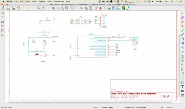
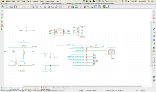
Designing a Schematic
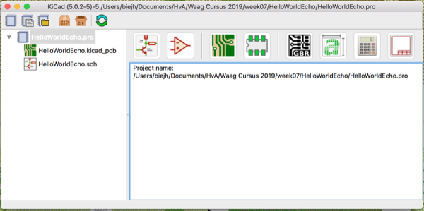
Start KiCad and open the EEScheme editor.
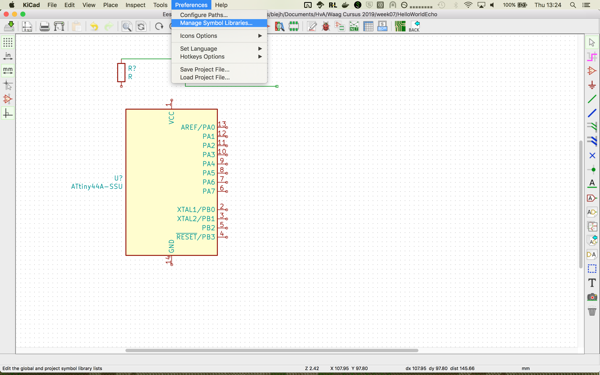
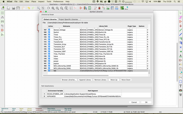
With our current design we need to load the fab academy library.
Load the fab library files in the libraries section of the scheme editor.
The files can be found at https://gitlab.cba.mit.edu/pub/libraries.
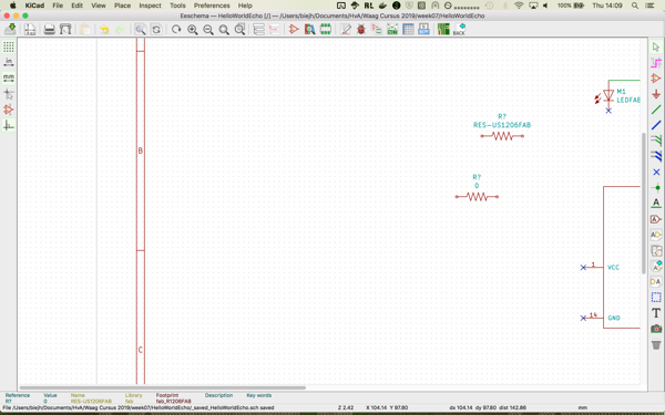
Select you components and connect them as desired.
If you want to connect components without making spaghetti, you can create a net-joint, a connection by name.
Simply assign a label to a wire that is the same as a label of another wire or component. For example assign the GND label for connecting the GND component.
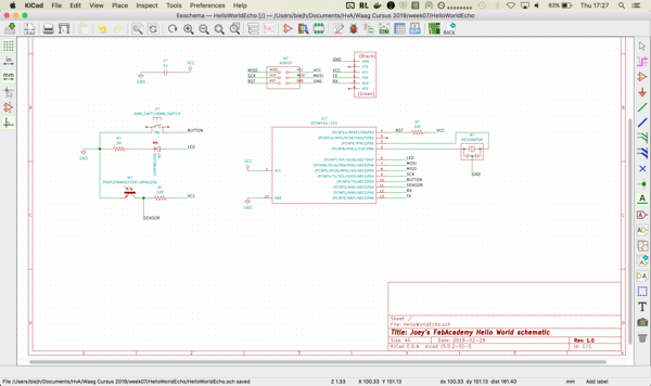
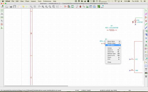
Also you can edit your component values if needed. For example you assign a resistor value by editing a resistor value.
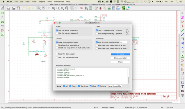
When you have placed your components and connected the wires you can assign names to your components by annotating them using the annotate option.
Open the annotation dialog, and first activate the clear annotations, then the assign option.
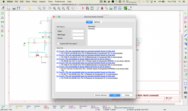
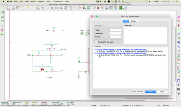
Next it is time to check if you properly connected all the wires.
Select the electrical rules checker. The software requires you to close the not used connections and will tell you what connections are not closed.
If you have unclosed connections. You need to close them using the close (X) option. Note that your will have the error: “Pin connected to some others pins but no pin to drive it” for the VCC and GND. This is normal, you can ignore those two messages.
From Schematic to PCB design
With KiCad you can create a PCB design from your schematic drawing.
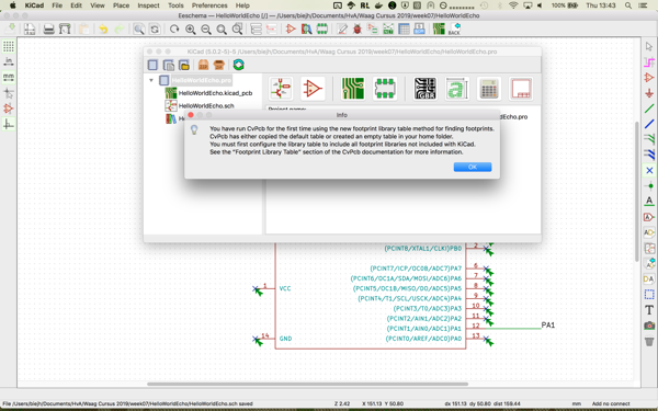
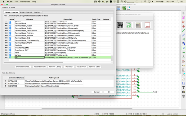
Before you start doing this you should make sure you have the correct library files for the components you want to design a PCB for, otherwise you will get “no footprint errors”.
In our case we need to import the component library from fabacademy.
The .pretty files can be found at https://gitlab.cba.mit.edu/pub/libraries/tree/master/kicad.
For importing open the PCB design tool and select the “Manage footprint libraries” in the Preference menu.
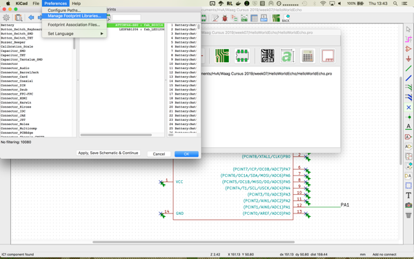
Note: If you are a touch pad (and OSX) user you might want to go to the preferences menu of PCB designer and check the touch pad scroll option. This make life with a touch pad much easier!
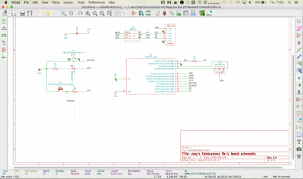
Having the needed libraries we are going to connect our components from our scheme to our PCB components.
Use the option “assign PCB footprints” and select the correct footprints for each component.
In our case these are the fab footprints.
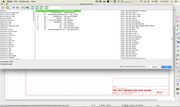
After matching all the footprints generate a netlist using the “Generate Netlist” option.
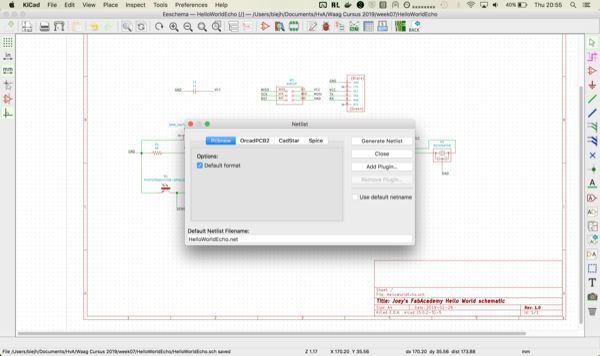
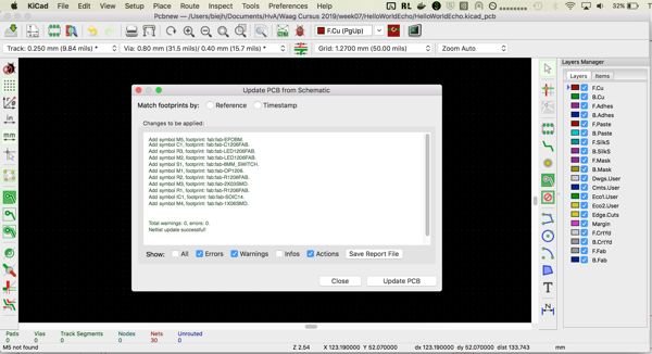
Go the the PCB editor and load the netlist you created.
Use the “Refresh from schematics” options from the tools menu to make sure you have the latest version of your scheme components.
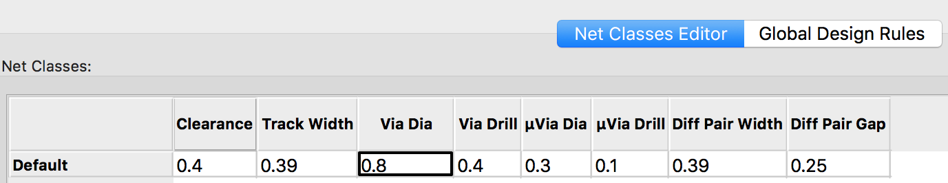
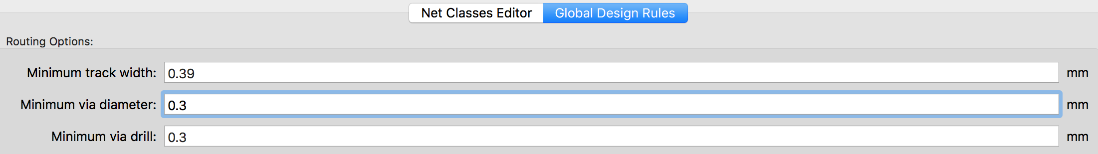
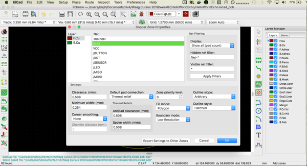
When you have your components first set your Design Rules
Set your design rules, either in Setup -> Design Rules… or in File -> Board Setup -> Design Rules.
The rules need to match with your mill. In our case we are using a 0.4 mm mill for our trace lines and 0.8 for our cutout, so our track with is 0.4 mm.
If you have a predefined board size, Define your boundary (size) of the board. If you can work in free space and let your board size depend on your traces, skip this step for now and define your board size in the edge cut layer at the end of your design.
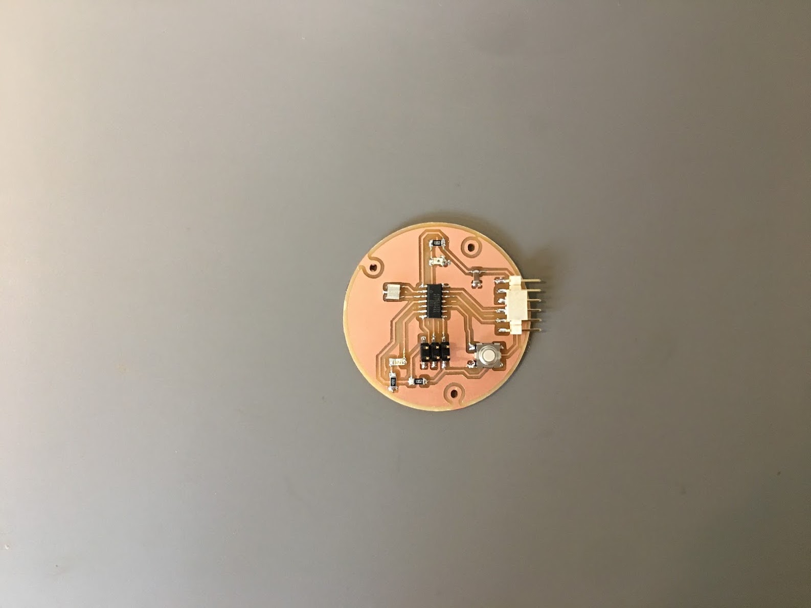
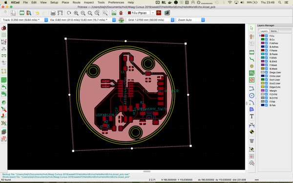
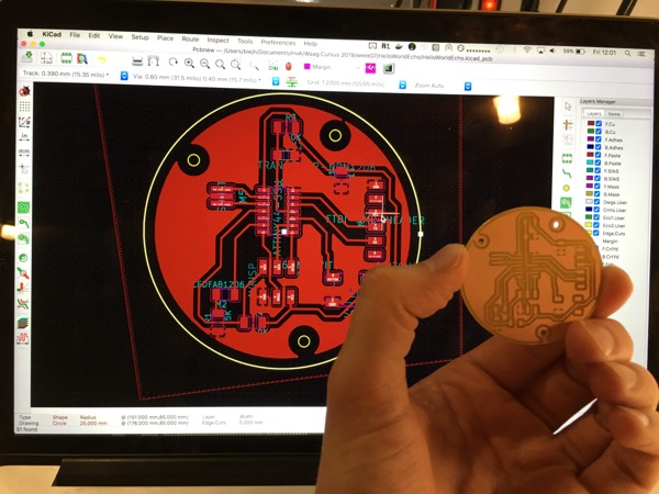
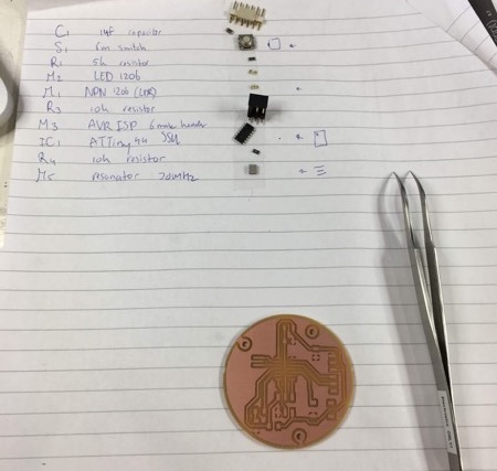
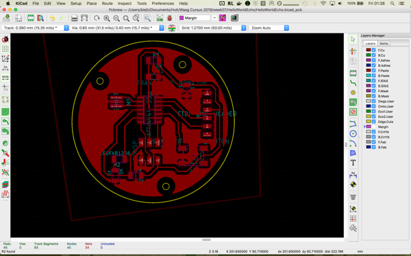
I decided I wanted to make a round board with mounting holes.
In the cutout layer I created a circle with a diameter of 30 mm.
An in that circle 3 smaller circles with a diameter of 2 mm.
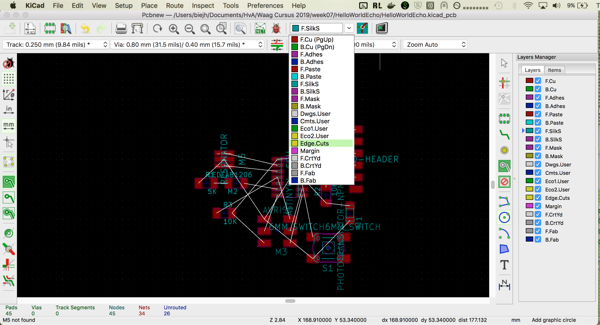
Note: Do not forget standard you will mill on the inside of your (cutout)line, make sure there is enough space between the cutout en the traces.
I noticed my cutout line was pretty close to the GND layer. To make the cutout less close I inserted a smaller cutout line recalculated the GND layer and moved the smaller line to the margin layer.
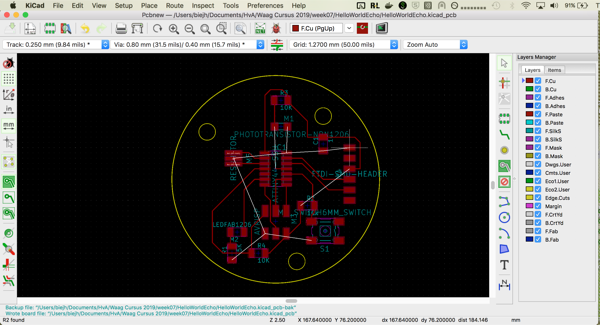
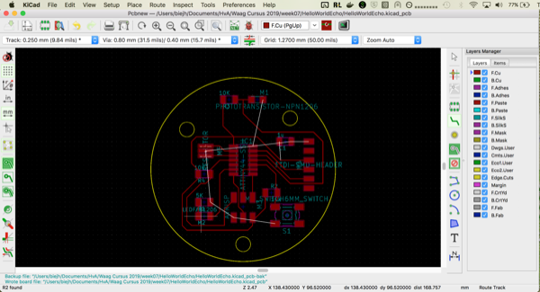
After loading your components, everything is cluttered at one place.
Place your components on the grid, take your time to properly place your components. This will make routing easier.
If you have different input and output components, make sure they do not interfere with each other.
For example I have a LDR and a LED. I placed the LED as far away from the LDR as I could.
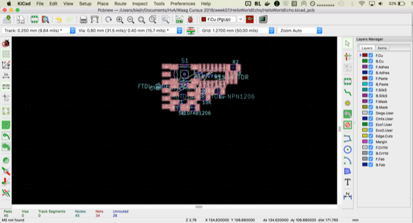
Route your connections, you can route by hand or using the auto route function.
Auto routing is not perfect. It is a difficult process, for small designs you are better of routing the lines by hand.
Leave the ground traces for last.
Tracing lines can be a big puzzle, if you really cannot create your design as desired you might want to create a bridge.
For creating a bridge, add a 0 ohm resistor by adding a resistor in your schematic, adjusting the value to 0, go to your PCB editor, update, and trace your line using the bridge.
For filling in the ground traces you can use all the copper of the plate as ground. This is called a Ground pore.
You can do this by use the “Add filed zones” function, and selection GND for the properties.
When Filling the zones for the GND, I noticed my circuits were not complete, I had several GND islands, making my traces not workable.
I connected the zones with a wire making the GND zones complete.
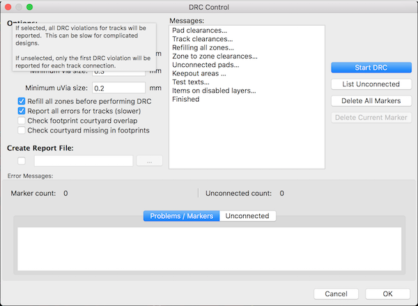
After you created all your traces make sure to check if there are no open traces left.
You can check by hand, white lines means missing connections, or check for open connections using the “Design rules check” ladybug button.
Note: If you have not defined your board size, do it know in the cut out layer as described previously, and replace your components if needed.
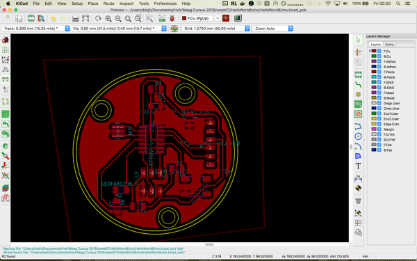
From Design to PCB
With fabrication outputs you can use for external companies producing your board. We will be creating our own board using the Roland mill and the mods software.
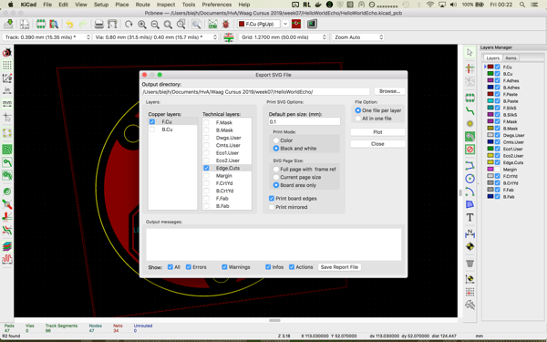
For the milling software you can export your design using the “Export as SVG” option in the file menu.
You need to export a cutout and a trace file.
For the cutout: First select the front copper layer, only black and white, and board area only.
For the trace file select the cut layer.
f.cu is the copper layer (your trace lines) and select edge.cuts for you cutout.
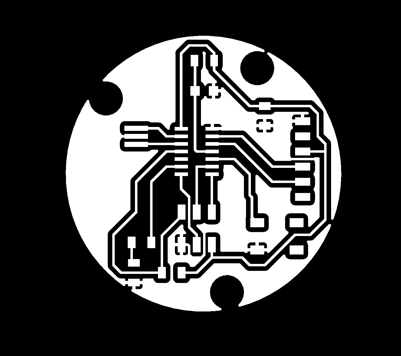


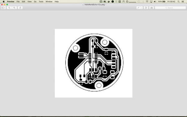
Our Mods software cannot read SVG files, so you need to convert the file to PNG.
I found a website cloud convert that can convert SVG to PNG at a decent quality (500 DPI).
For mods the trace file is still not correct, you need to invert the colors.
I inverted the colors for the cutout using the OSX Preview app. This made the trace lines white. When converting the image again in mods I had the correct end result: black lines with a white background.
For the cutout holes I edited the cutout file to only 3 black dots for the holes.
For the complete cutout, I edited the cutout file to 1 big black circle.
Both edits were made in the OSX Preview.app
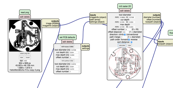
I tested the PNG’s in mods on my own computer.
When I copied the files to the computer for the Roland mill, the mods software did not processed the trace out file correctly.
I saved the correct processed PNG from my mods version copied it to the Roland mill computer.
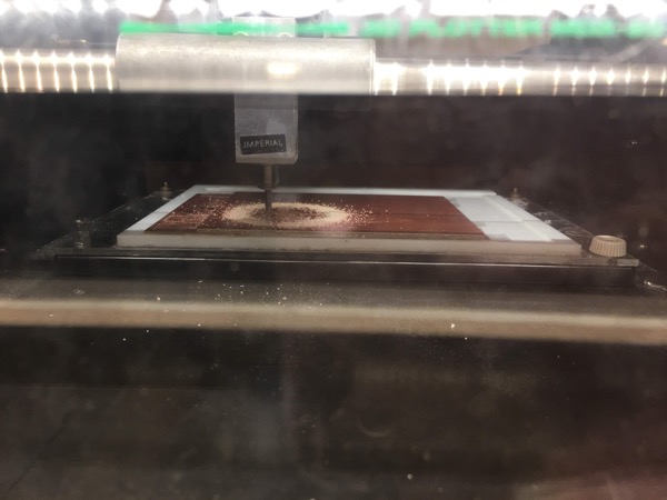
For the milling I followed my tutorial made in week 5.
I noticed not all the steps were detailed enough on settings, and modified them thanks to my new experience or from input from the group.
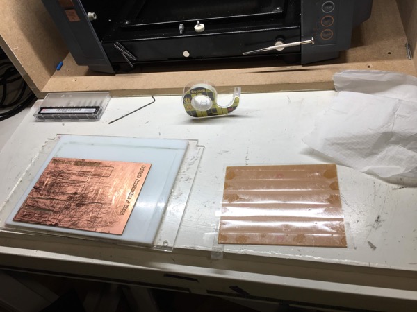
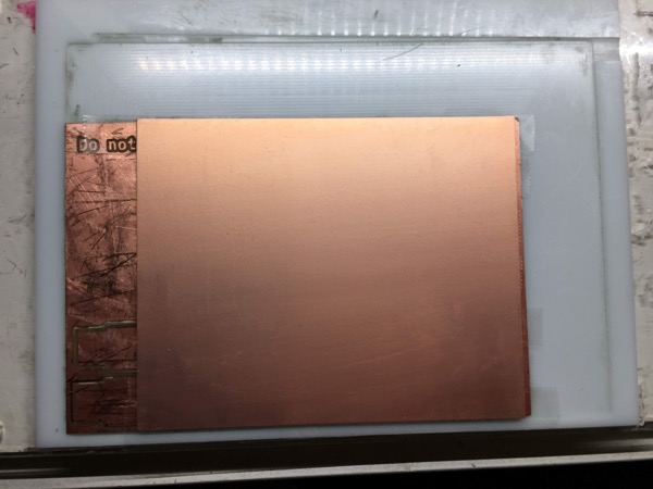
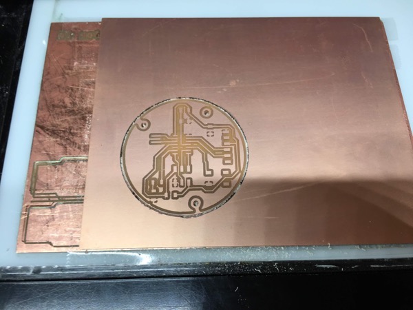
I took the basic steps: cleaning the baseplate, placing a new copper plate, calibrating the mill, and milling.
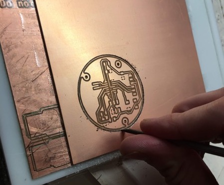
Removing the PCB from the copper was very difficult. A round PCB sticks better to the tape, and I had to circulate the screwdriver twice around the PCB to be able to remove it without breaking the PCB.
Last I compared my mill with the design to see if traces were missing, this was not the case!
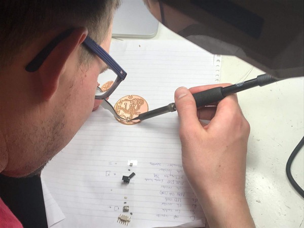
Soldering the PCB
Again following the steps from week 5:
I removed the excess material with a knife and tweezers.
I cleaned the board with soap.
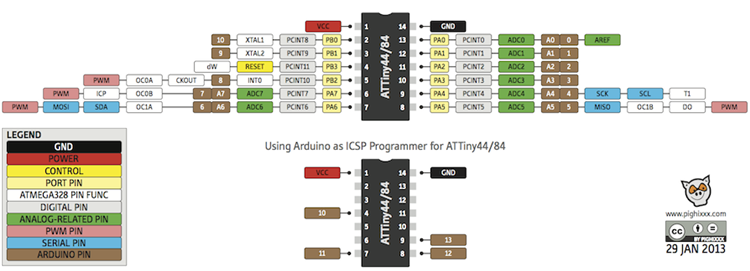
Gathered the components and looked for their correct orientation using data sheet of the Attiny44 datasheet and the PCB design I made. For the button I used the datasheet found here and used a voltage meter to double check how the pins are connected.
Finally I tested the button with a voltage meter to find its correct orientation.
For soldering I first soldered some easy components (LDR and resistor) to get familiar with the process again.
This was a good idea, I soldered the components in the wrong place, and it took me two components to get back in the solder-flow again.
After the two components I started from inside to the outside, starting with the ATTiny and finishing with the button.

Checking if the board works
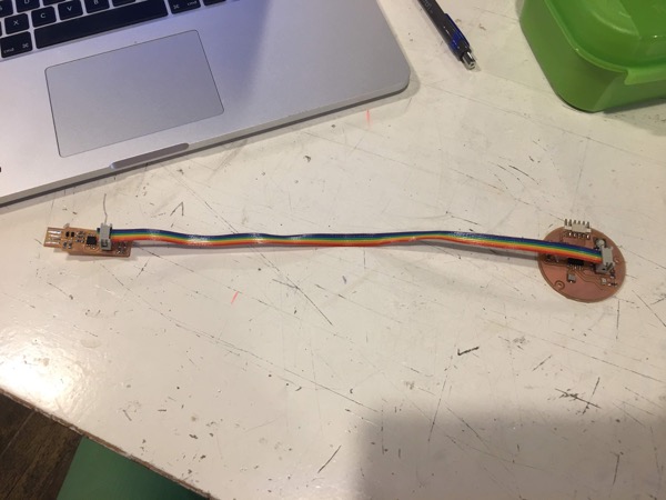
After soldering I connected the board to my programmer and connected the programmer to my computer using a usb2.0 hub.
To see if my programming board was detected I used the command line
C02KR0SBFFRP:HelloWorldEcho biejh$ ioreg -p IOUSB
+-o Root  <class IORegistryEntry, id 0x100000100, retain 15>
  +-o Root Hub Simulation Simulation@14000000  <class AppleUSBRootHubDevice, id$
    +-o Apple Internal Keyboard / Trackpad@14400000  <class AppleUSBDevice, id $
    +-o BRCM20702 Hub@14300000  <class AppleUSBDevice, id 0x100010308, register$
    | +-o Bluetooth USB Host Controller@14330000  <class AppleUSBDevice, id 0x1$
    +-o USB3.0 Hub@14600000  <class AppleUSBDevice, id 0x100011e45, registered,$
    +-o USB2.0 Hub@14200000  <class AppleUSBDevice, id 0x100011e63, registered,$
      +-o USBtinySPI@14210000  <class AppleUSBDevice, id 0x100011e7e, registere$
Then I checked if the programmer could talk to the ATTiny44 on my board using the AVRDUDE command
C02KR0SBFFRP:HelloWorldEcho biejh$ avrdude -c usbtiny -p t44

avrdude: AVR device initialized and ready to accept instructions

Reading | ################################################## | 100% 0.00s

avrdude: Device signature = 0x1e9207

avrdude: safemode: Fuses OK (H:FF, E:DF, L:62)

avrdude done.  Thank you.
Success! I have a working board!
I also checked without the wire connected, to see if it really could talk.
C02KR0SBFFRP:HelloWorldEcho biejh$ avrdude -c usbtiny -p t44

avrdude: initialization failed, rc=-1
         Double check connections and try again, or use -F to override
         this check.


avrdude done.  Thank you.
Group assignment
For our group assignment we had to:
“use the test equipment in your lab to observe the operation of a micro controller circuit board”
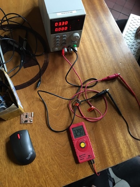
For this assignment we used:
- a regulated digital controlled DC power supply.
- a voltage meter
- a digital oscilloscope
Regulated Digital Controlled Direct Current Power Supply
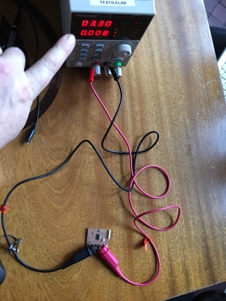
As can be seen om the photo a regulated digital controlled DC power supply allows you to provide a specific voltage and current.
The top indicator is the voltage, below is the current in ampere.
For our current board we set our voltage to 3.3 volt and current to 0.5 ampere. (Typical electrical equipment with micro controllers, will not draw higher than 1 or 2 ampere.)
As with all electrical components, make sure you know their minimum and maximum load. If you do not know for sure and need to guess, you might notice you guessed wrong when something start smelling or smoking.
When you connect the power supply to your device, it will show how much current the device is drawing.
As with all electrical equipment always first connect the ground (in this case the black cable).
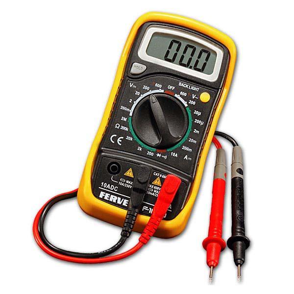
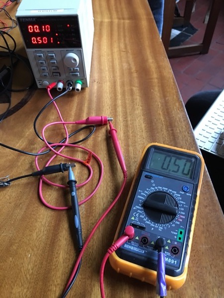
Multimeter
A multimeter allows you to check voltage, current and resistance. Also you can check for connections, using the connection option. This is often indicated with a speaker icon.
When you are unfamiliar with the used equipment as the used power supply check the output with a multimeter.
When connecting the multimeter always first connect the ground (in this case the black cable).
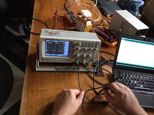
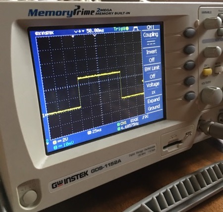
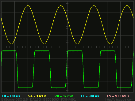
Oscilloscope
An oscilloscope allows you to measure the signal on a line in frequency or over time.
For example you can not only see if there is an active signal on the line, you can also see if it is a digital (only high or low) or analog (a wave form) signal.
You can see the frequency of the output, and using the various options, zoom in/out on the signal, detecting the various waves off the signal.
In our case the small turning knobs are for moving on the vertical and horizontal axis and the large turning knobs for defining the scale.
Our oscilloscope allows us to connect two signals, but in the current example we only connect one.
Always first connect the ground, in this case it is a small hook attached to the signal wire.
Then connect the large hook to the active wire you want to measure the signal on.
A typical digital signal (high/low) on the oscilloscope
Fails
No pull up?
I always thought you should not directly connect your outputs to the ground, always put a resistor in between to avoid a shortcut.
The schematic we were given a schematic with a button that is directly connected to ground and when not pressed leaving a floated pin on the IC.
I checked the Attiny44 datasheet
and did not saw a special feature to correct for this floating pin, so
I redesigned the connection to a pull up resistor circuit. as defined here by resitor guide and here by sparkfun.
For a 3.3V circuit I use the formula Resistorvalue (ohm) = Voltage / Current (amp)
3.3 / 0.001 = 33k ohm resistor
But after reading some online fora regarding appropriate resistor values for 3.3V circuits, I found that most people tend to use 5k or 10k resistors, and that also works. For now I will try 10k resistor, and only replace with higher if this does not work.
It turned out to be all a waste of time. After talking with Henk, I found that I did not check the datasheet correctly, and the ATTiny does have a pull up feature that can be used, so no extra resistors are needed.
Convert SVG to PNG via Imagemick fail
For converting the SVG export file to PNG I used Imagemick. This was a big fail, I noticed a lot of detail in the image was lost.
C02KR0SBFFRP:HelloWorldEcho biejh$ convert HelloWorldEcho-F.Cu.svg HelloWorldEcho-F.Cu.png
C02KR0SBFFRP:HelloWorldEcho biejh$ convert HelloWorldEcho-Edge.Cuts.svg HelloWorldEcho-Edge.Cuts.png
I tried also the convert statement with -quality 100% , this did not gave other results.
I decided to try an other tool and found a website cloudconvert that can convert SVG to PNG at a decent quality (500 DPI).
Confusing diameter with radius of circle

During designing the board I made the mistake to confuse diameter with radius, so I accidentally designed the board twice as big as intended.
After I found out this error in thinking, I reduced the radius and replaced and retraced my components and wires.
Scheme rules check error with GND and VCC
After closing the connections I still had markers at the GND and VCC components with the error: “Pin connected to some others pins but no pin to drive it”.
I tried to redraw the connections, this did not resolve the error.
I thought it could be because of the duplicates of the VCC and GND. So I deleted the duplicates and joined the end of the wires to the VCC and GND components using the label markers. This also did not resolve the errors.
After some searching I found there are many problems with power and ground as can be read on this post.
I tried the solution of adding a Power Flag, as suggested in the blog post. In stead of resolving the error, it gave new errors: “Conflict problem between pins”.
After going through this tutorial, I found that my error is a problem due to how the IC in and outputs are defined and I do not have to worry about this problem. So I went on with my design ignoring the errors for the GND and VCC.
PCB footprint error
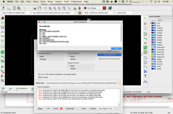
Not correctly connected the components in the scheme editor to the footprints.
This resulted in no footprint errors in the PCB editor.
After reassigning the components to the footprints and updating the PCB editor from schematic the errors were resolved.
Zones not connected
When Filling the zones for the GND, I noticed my circuits were not complete, I had several GND islands, making my traces not workable.
This was easily solved by connecting the zones with a wire.
Milling using full image not only trace lines
When milling my image, unfortunately the mill used a lot of empty space before milling.
This was because my export image contained large empty sections around my cutout, the mill included these empty sections with the milling.
It was difficult to see when only looking at the trace lines, and when I noticed this, I had already milled a part from the copper.
Next time I would make the margins around my cutout as small as possible.
Milling lines not visible for mods
When I tried to remove the margin around my cutout, I selected the cutout and cropped the image around the cutout (in the OSX Preview app).
This cropped image did not work in the mods software. It turned out you always need a small margin left for the software to be able to trace the lines.
Soldering the components in the wrong place
For soldering I first soldered some easy components (LDR and resistor) to get familiar with the process again.
This was a good idea, I soldered the components in the wrong place. I noticed I had to carefully look at the PCB design to clearly distinguish the components from each other. After this fail, fortunately I had no wrong components.
Reflection
I really liked the KiCad software, although it has many options, the steps to take are logical and well designed.
Much can go wrong, but I encountered only minor issues. I took great care in my design and in every step of the process, and next time I would also take the time to create my design, preventing me from making errors.
It was difficult to determine the actual distance between the components. After creating the board I concluded I left to much space between the components and in a next version I would place the components closer to each other.
Also (as described in my fails) next time I would better reduce my margins of my trace and cutout files to reduce the waste of copper.