characterize the design rules for your PCB production process
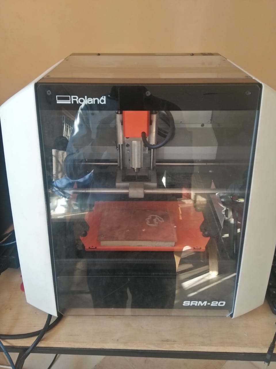
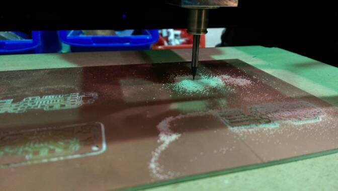
We started to practice using the milling machine Roland SRM-20 with our whole group in the noon of 15.2.2018.
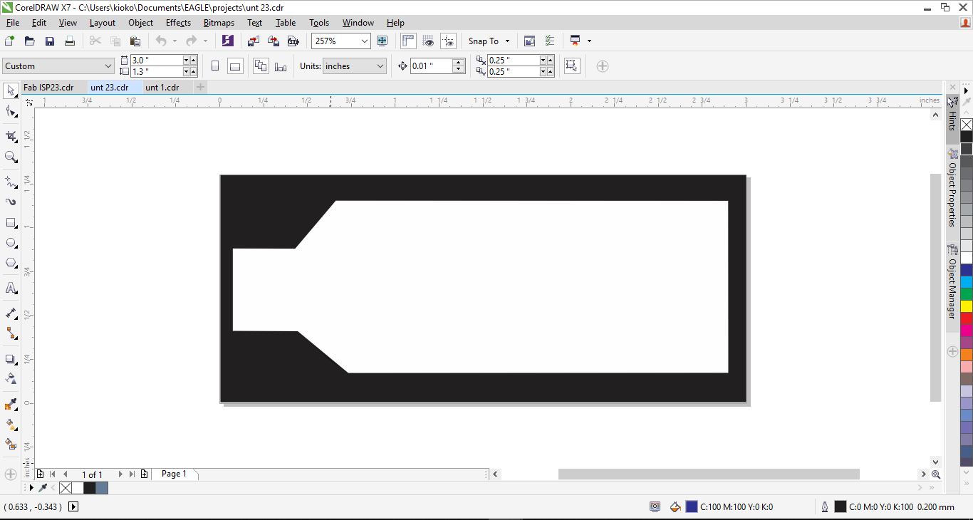
preparation of the input files for the milling machine. The input files are made in
make an in-circuit programmer by milling the PCB, program it, then optionally try other PCB processes
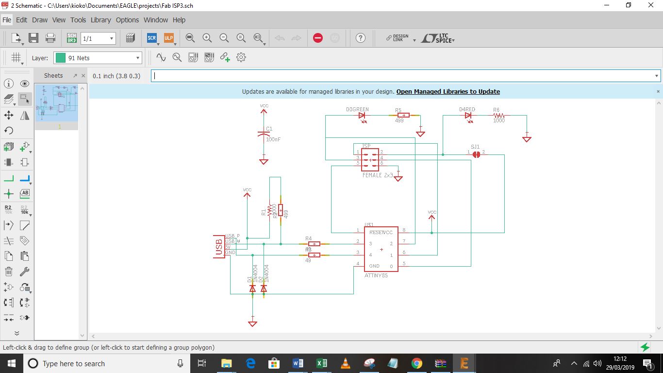
This week, i built an In-System Programmer (ISP), which is used to program other microcontrollers that are already built into their circuits..
Electronics Design week,and in other weeks).
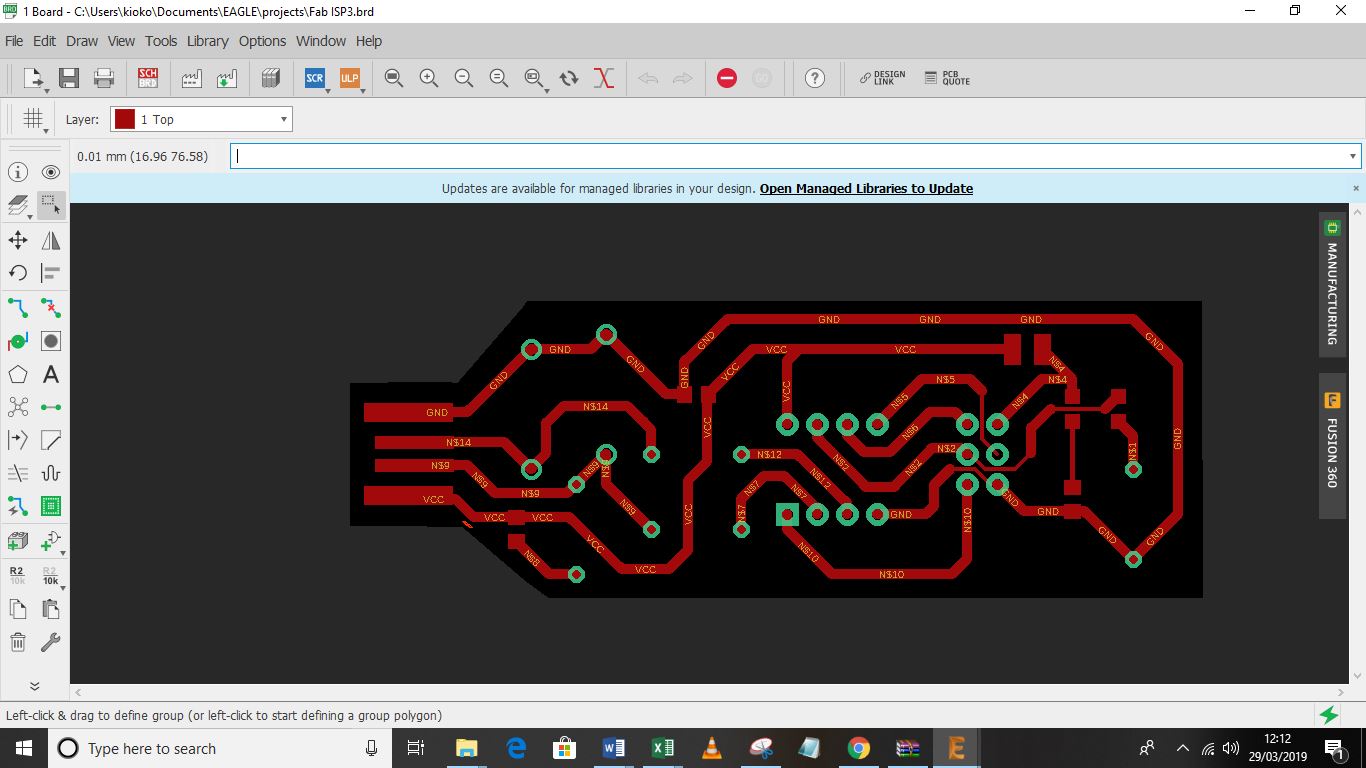
After download the designed PNG from class webpage i generate the Roland Mill file using Fab Modules.
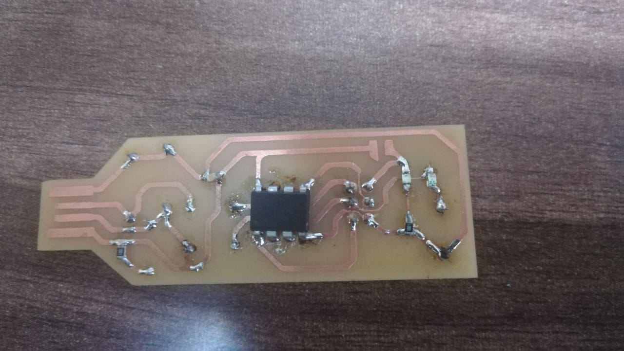
I milled the board using the Roland SRM-20 Modela mill.
First of all we made a solid and uniform base using a 1mm milled SANMODUR blocking it on the workspace with double-side tape.
For milling the traces I used a 0.12mm conic tip (bolino) with 40° angle inch bit,
to remove all copper from the usb connector i used a 0,4mm tip,
while for cutting out the board i used the 2mm tip.
.jpg)
I have used Fabmoduls to generate the files needed for the machine in our lab.
I have upload the PNG traces file on Fabmodules
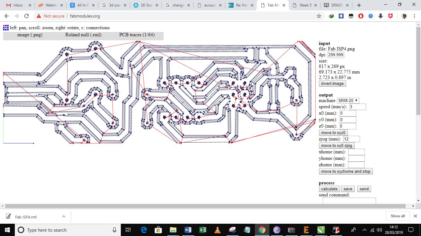
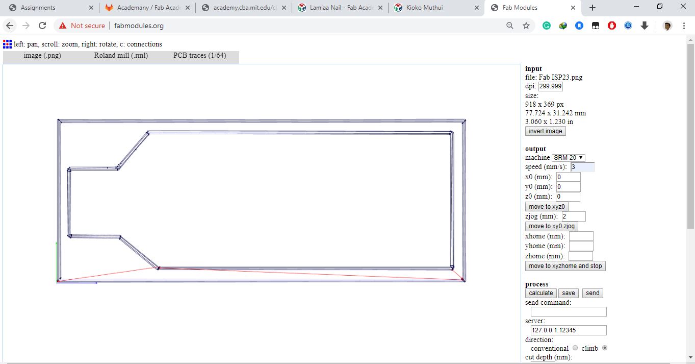
after the machine is done i did the same for the Outline but instead of Choosing
Traces (1/64) i Chose Outline (1/32). then pressed Calculate.
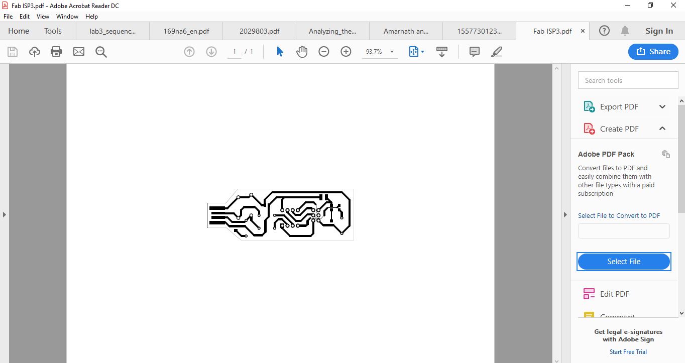
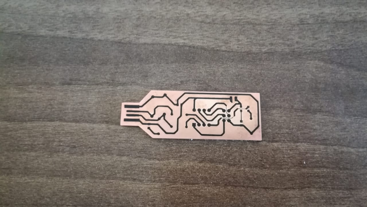
Result
After milling I have washed my board with soap and water to
remove waste material and allow solder material sticks better.
Soldering is the process of connecting electrical components to one another or to a conductive substrate.
We are using smd(surface-mount device) for this.
While gathering the smd's I wrote the components as follows
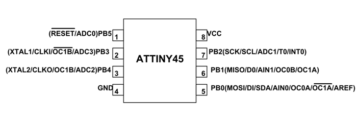
1 ATTiny 45 microcontroller
1 Capacitor 1uF
2 Capacitor 10 pF
2 Resistor 100 ohm
1 Resistor 499 ohm
1 Resistor 1K ohmv
1 Resistor 10K
one 6 pin header
1 USB connector
2 jumpers - 0 ohm resistors
1 Crystal 20MHz
2 Zener Diode 3.3 V
1 usb mini cable
1 ribbon cable
two 6 pin connectors
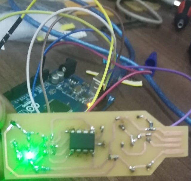
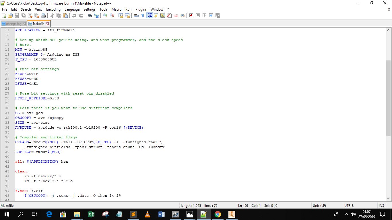
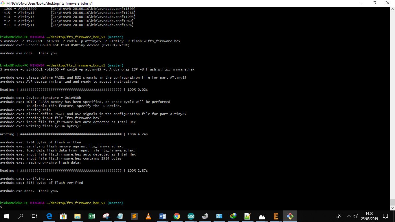
Then i run the make flash command