Final Project phase 06
state: week13
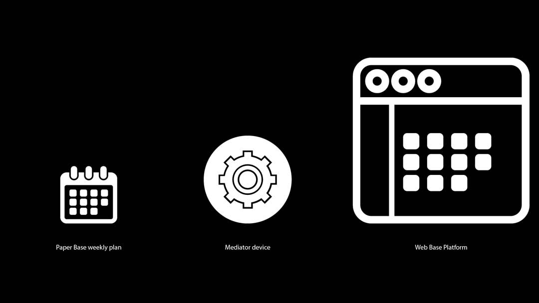
Doubting my final project since it is too ambitious and with being out of lab for more than 2 month I got afraid about how I would be able to prototype and progress on it. So I was thinking to have alternative final project which can full fill remotely. I planned to reduce the fabrication size.
My initial idea for this is a dashboard where people can have live stream of the food supply network in their neighborhood.
The other path that I could take is to focus on one of the systems of my vending machine. for instance the device which can recognize the fruits through the computer vision.
Also I am thinking of making a physical board for weekly planning which will be automatically transfer the time blocks in a digital calendar.
state: week16
I finally decide to go with the calendar. I start with the CAD design of it. But for sure it needs couple of iteration to improve the design.
Motivation
I used to plan my ahead week which involve writing things down and then transfer it to an online platform. or sometimes I just use the online platform but it is not fun process. So I would like to make a physical interface for my weekly plan where I gamify the process of planning. First It could be always on my table so I do not need to use my phone or open a tab in browser to find out my plan. If I need to adjust I would just change some elements instantly. Furthermore, Having a physical plan provoke me to stick to it more than a web base.
How it is working?
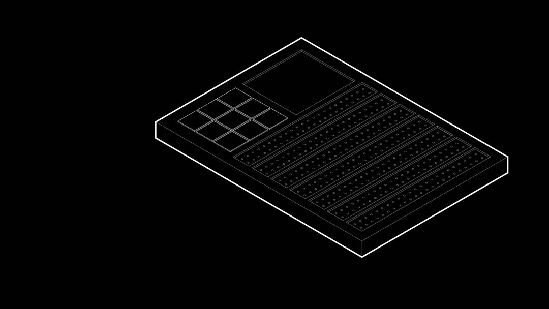
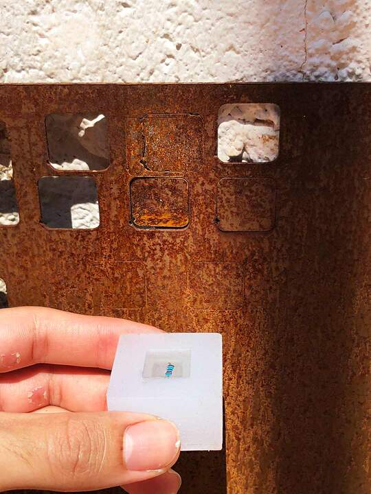
It is very simple you will assign a planes to each color and when you put this plan on the board the LED beside it will take the color. Each block of planes actually is a resistor. In fact by assigning colors you are basically assigning a resistor value to that plan.
Concept Demonstration
Electronic design
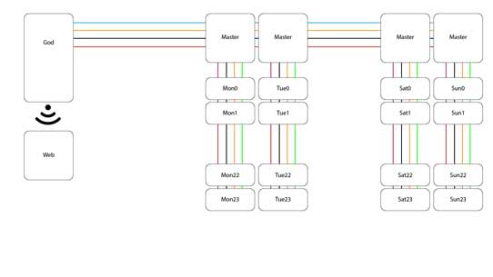
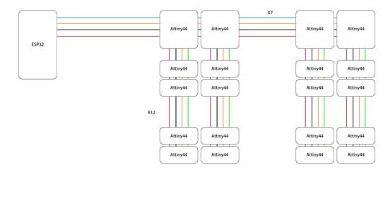
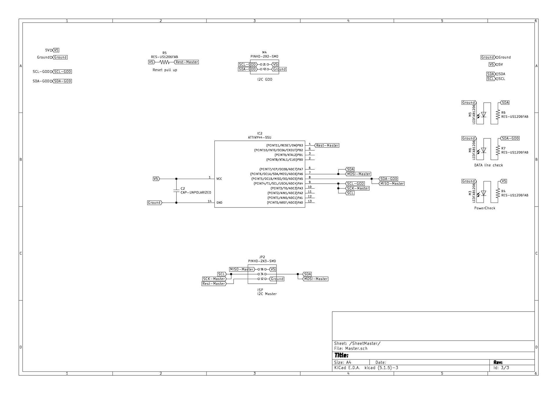
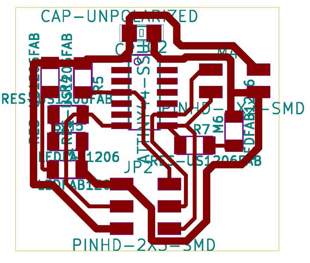
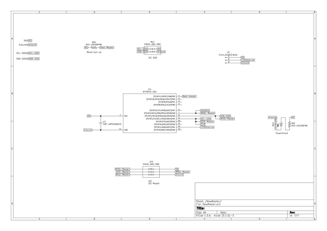
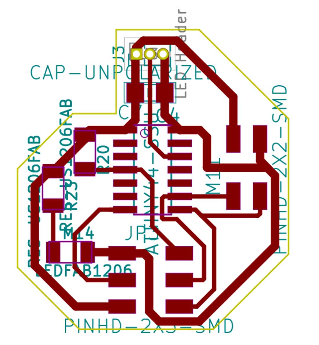
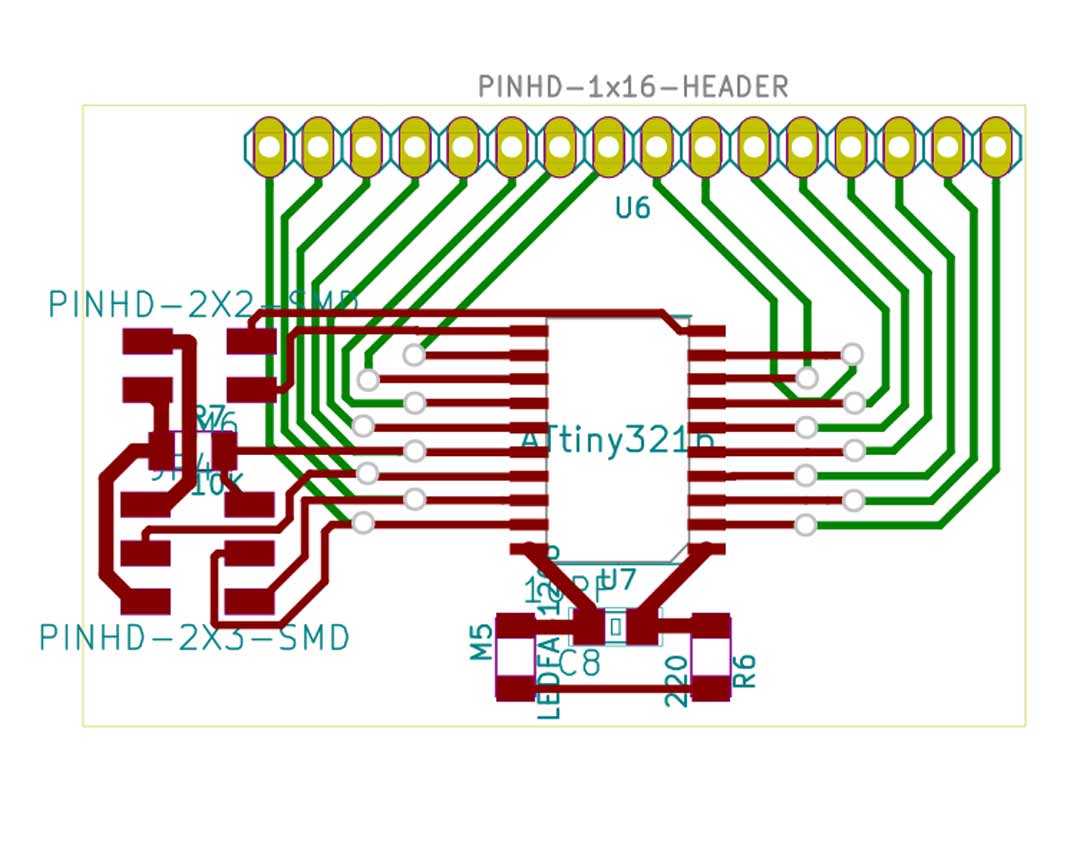
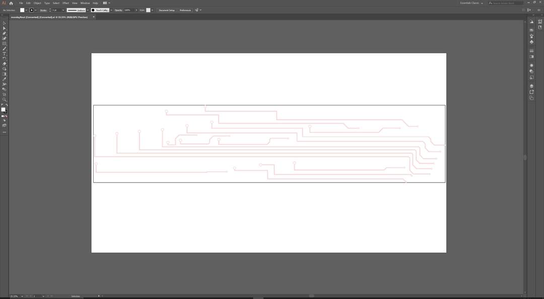
As You can see in the system explanation I have been used attiny44 for slaves and masters and ESP32 for the Main board. Here is the schematic design and PCB design for this boards.
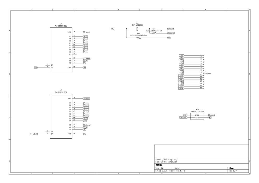
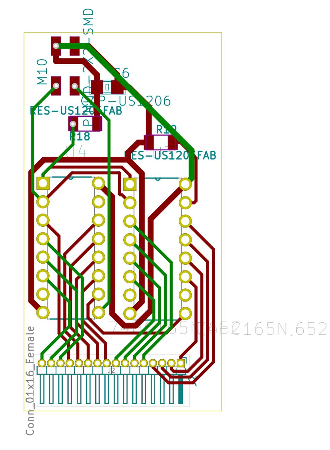
After further discussion with my instructor we reach start rethink the method of communication between master and slaves. Instead we can use shift register to increase the input pins of the master and avoid producing 60 slave boards.
What has been done
- google calendar on ESP
- google calendar Arduino lib
- google calendar / weather dashboard
- ESPaper calendare
Application and implicationNew
for new Project
link to previous project
Masterpiece
As I define the masterpiece in the previous assignment it should present skills and knowledge of its creator. So in this project I have tried to pass through what we learned and push the bar higher than the assignment requirement.
What will it do?
It is a bridge between our paper base planning and digital calendar which give you a physical interface
Who’s done What beforehand?
You can find the links to couple of project that tried to make device to communicate with google calendar above this section.
What will you design?
What parts and systems will be made?
Short answer: EVERYTHING
Long answer:
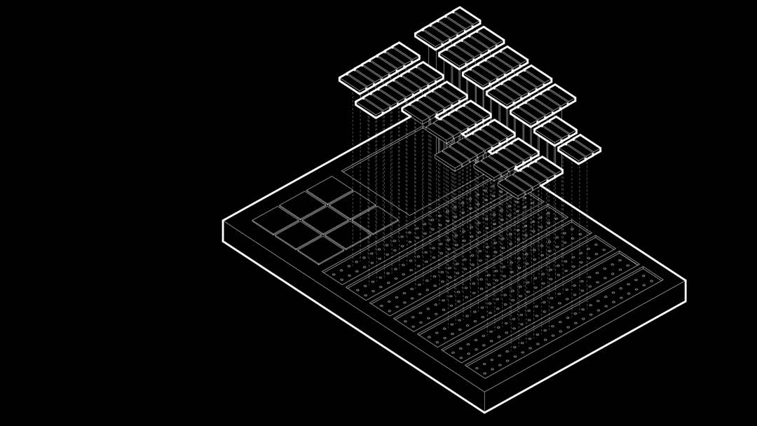
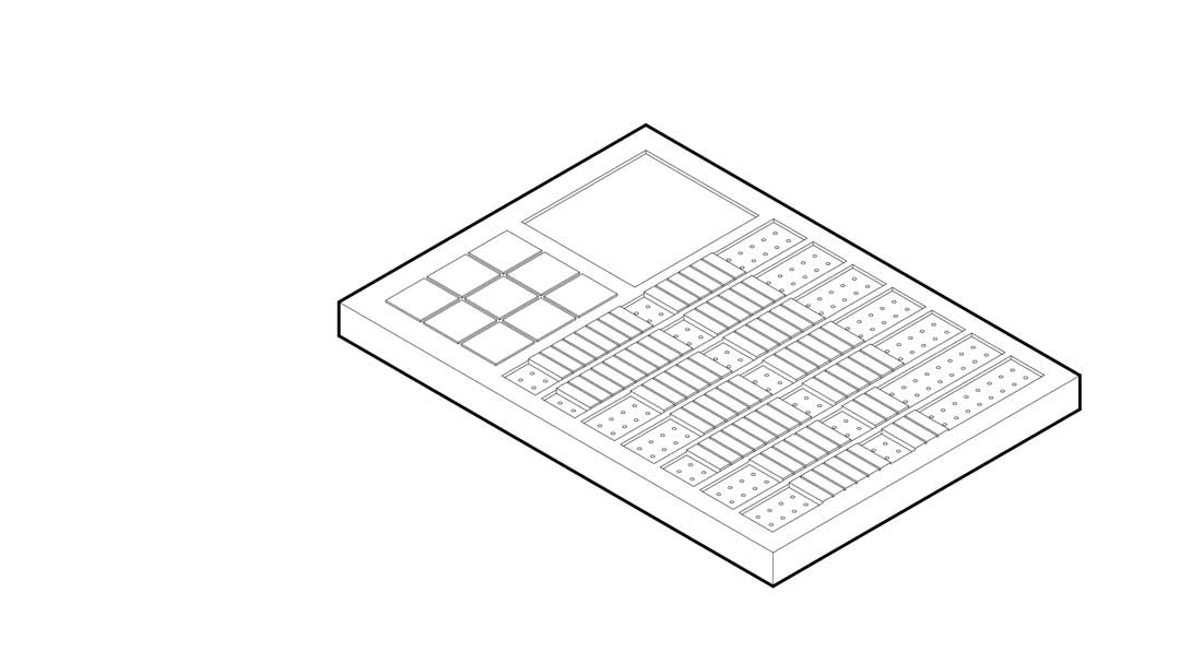
I have start the design from the smallest part of the project which is the buttons that I am gonna use as program/Schedule. Then I continue with the electronic design which consist a main board and 7 slave board. This followed by the designing the panel where the blocks will be plugged. After this a frame and back plate designed to embed all the systems in itself. At the end a stand is designed to hold the panel on the table with adjustable angles.
What materials and components will be used?
Where will come from?
How much will they cost?
| Material | specification(mm) | quantity | Provider | cost |
|---|---|---|---|---|
| Plywood | 5005009 | 1 | Local/ Recycled from lab | |
| Bendable Plywood | 2654005 | 1 | Lab inventory | |
| Transparent Acrylic | [100603 | 0.5 | link | 14 |
| Transparent Acrylic | [100605 | 1 | link | 44 |
| PLA Filament | 230g | Lab inventory | ||
| Resin | 100ml | Lab inventory | ||
| Wax | 1468830 | 1 | Recycled from lab | |
| Silicon | Platinum Rubber silicon | link | ||
| ESP32 | 1 | link | 3.46 | |
| Attiny3216 | 7 | link | 1.04 | |
| Copper vinyl | 100*400 | 1 | Lab inventory |
What processes will be used?
- 2D and 3D CAD modeling
- electronic production
- Machine control cutting
- 3d printing
What questions need to be answered?
does it work?
does it have understandable interface?
does it represent my skills and capability to use digital tools?
Fabrication processes
Since I changed my project did not have enough time to prepare the designs for it I did the design while I was fabricating. To make sure every elements are working together I have used bottom up approach for my design and fabrication processes. In this manner I started the project from defining the smallest elements and adjust the overall design through the course of fabrication. Also I have tried to do the processes that have more risks of errors at first so I would have time if anything goes wrong.
Molding and Casting
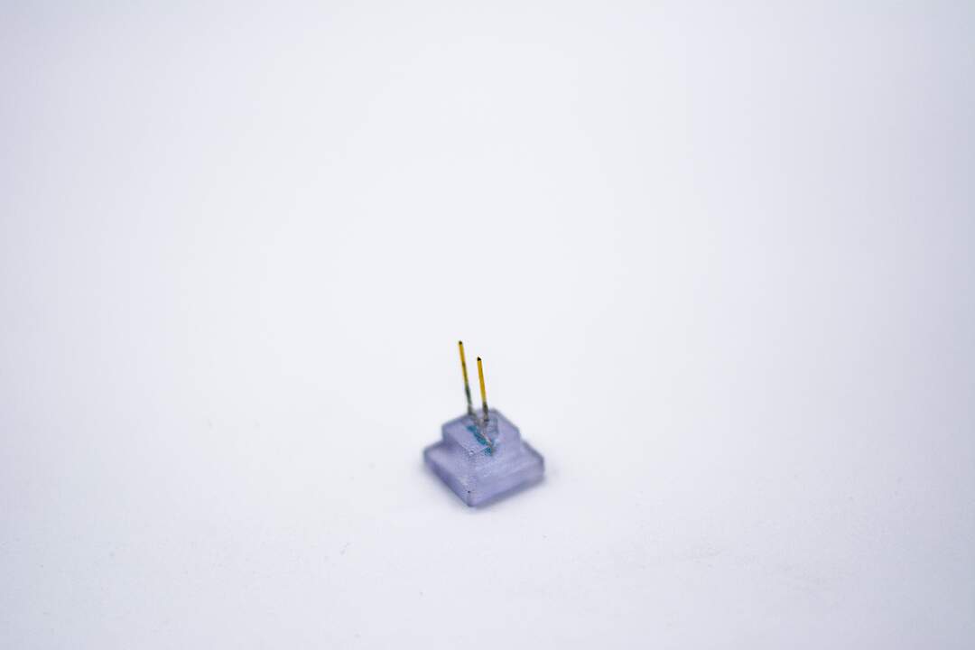
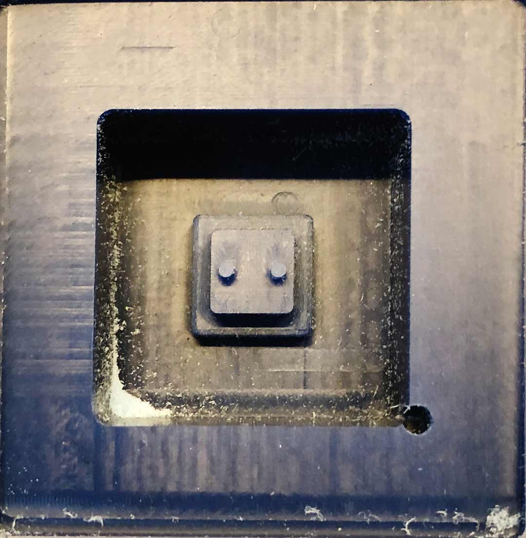
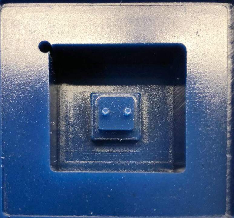
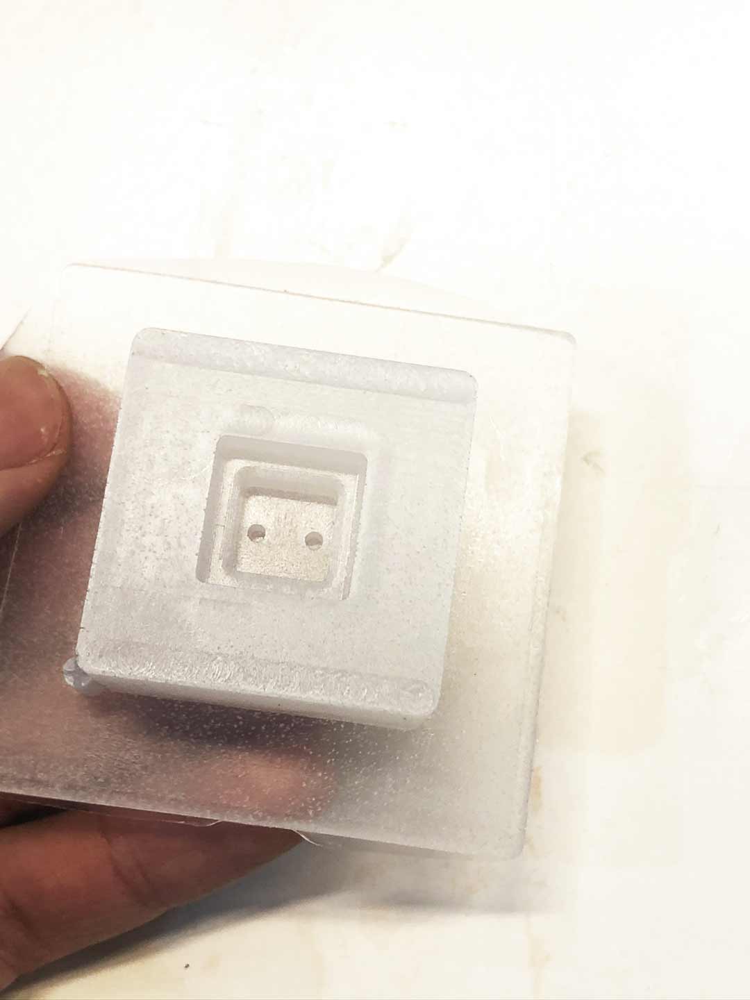
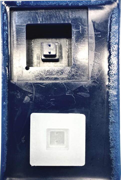
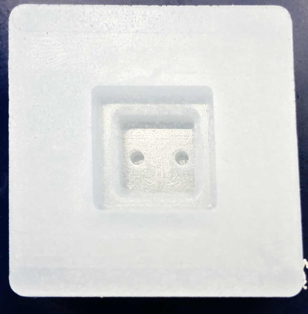
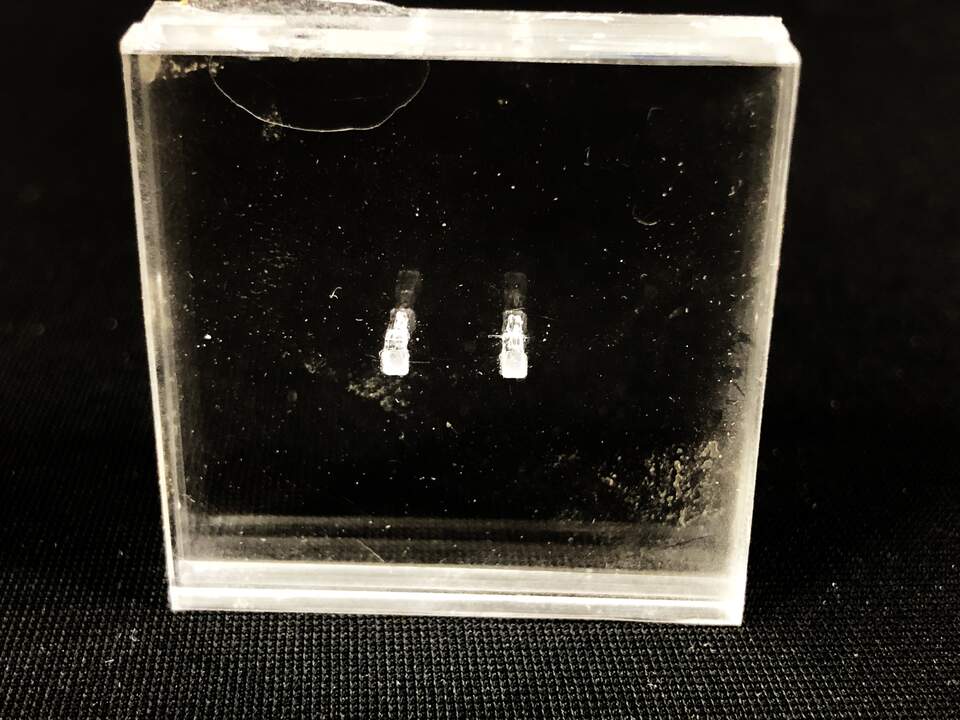
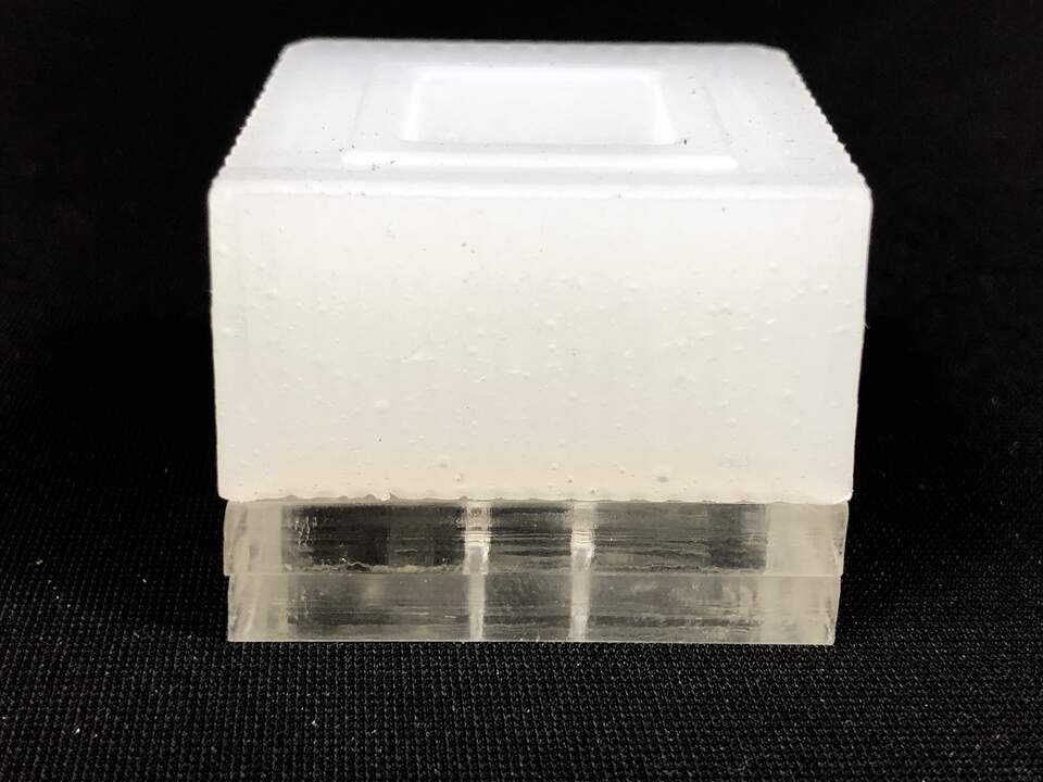
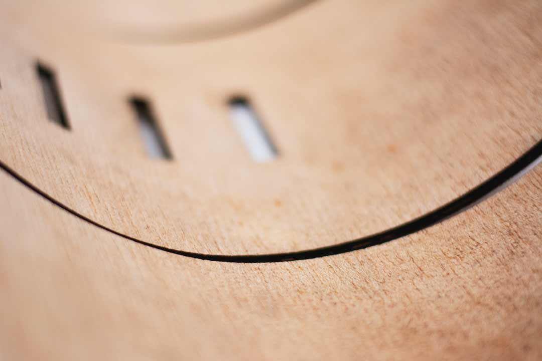
I used this fabrication method to make the time blocks of may project. After few iteration of the design I finalized a shape and prepare the file for the CNC. Since I needed the final part to be hard and transparent I choose clear resin for Casting. Base on this choice I needed to make my mold with soft silicon. In order to make the silicon mold I needed to cast silicon in a wax mold from my positive object. One of the challenging part of this process was embedding a resistor inside of each blocks.
File preparation
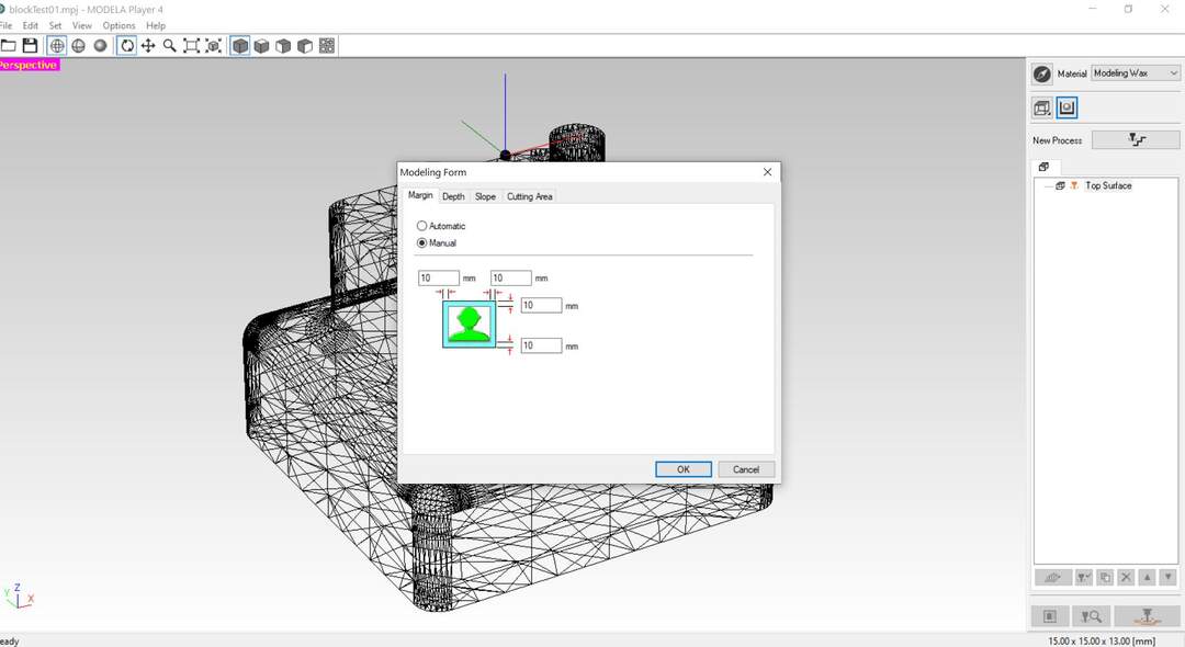
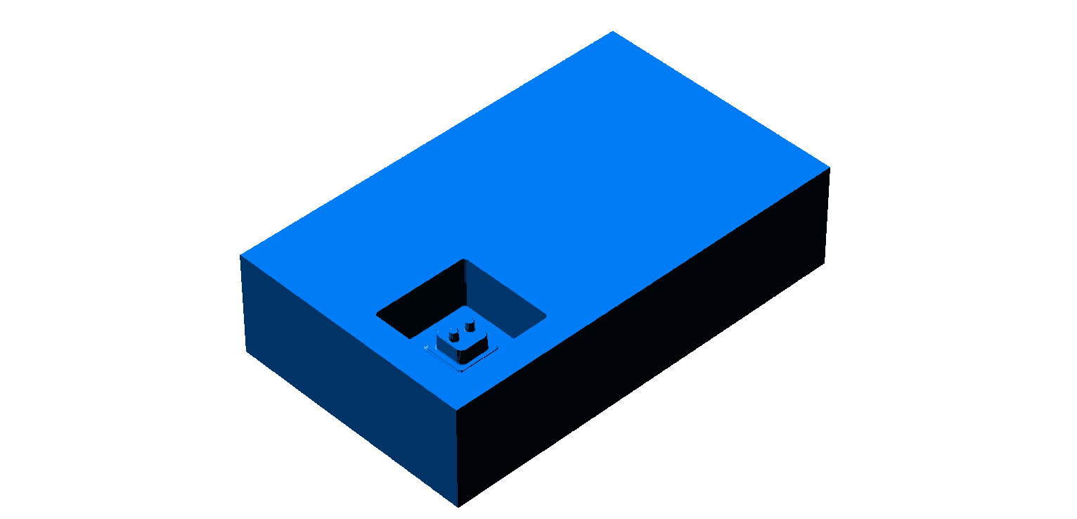
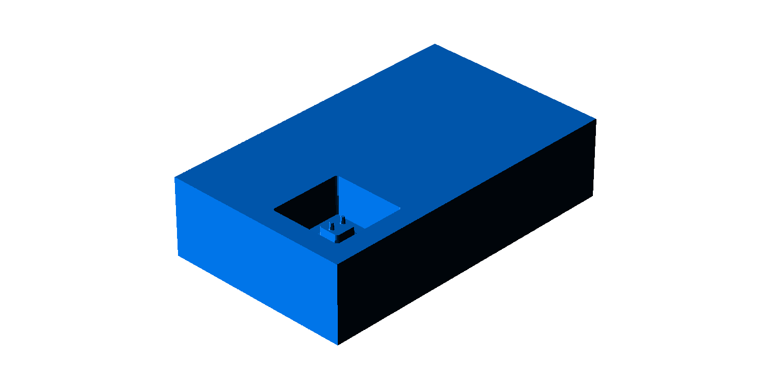
For the file preparation from the 3D of the block I needed first to make the 3D of the silicon mold which was a Boolean operation between a box and my object. The placing of the object and the margins from the box edges are very importance because that will help to keep the silicon mold solid to enough to not deform while casting resin. Next stage is to Boolean the silicon mold from the wax to have the shape for CNC milling. Again positioning here also is important. I put a margin of 10 mm from edges of the wax brick to make sure it will not break during the casting and machining processes. In addition the thickness of the bottom part of mold after CNC shouldn’t be less than 10 mm. It would be good practice to make the walls of the mold a bit in angle to avoid crash of spindle’s collet into the wax. Also it would be great if you check the length of the milling bit and the depth of your design in order to avoid collisions.
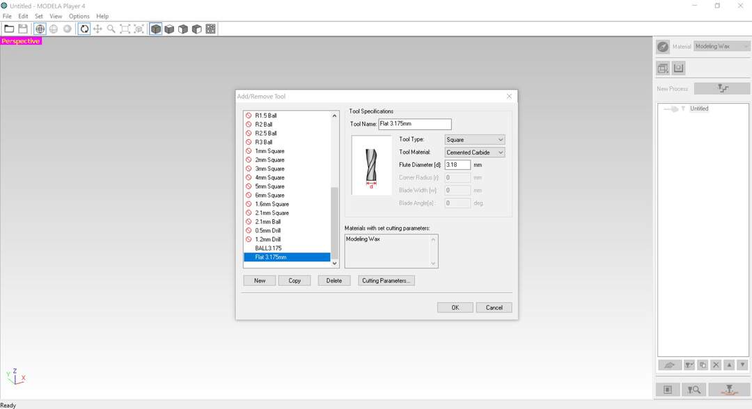
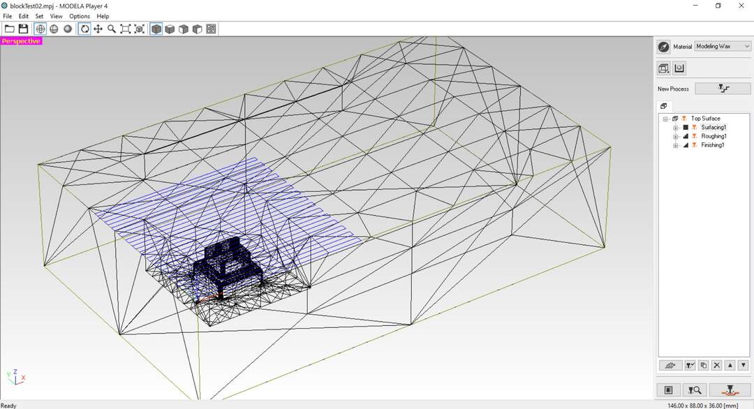
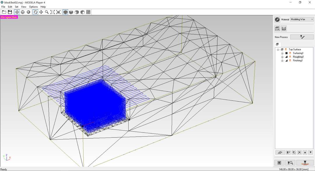
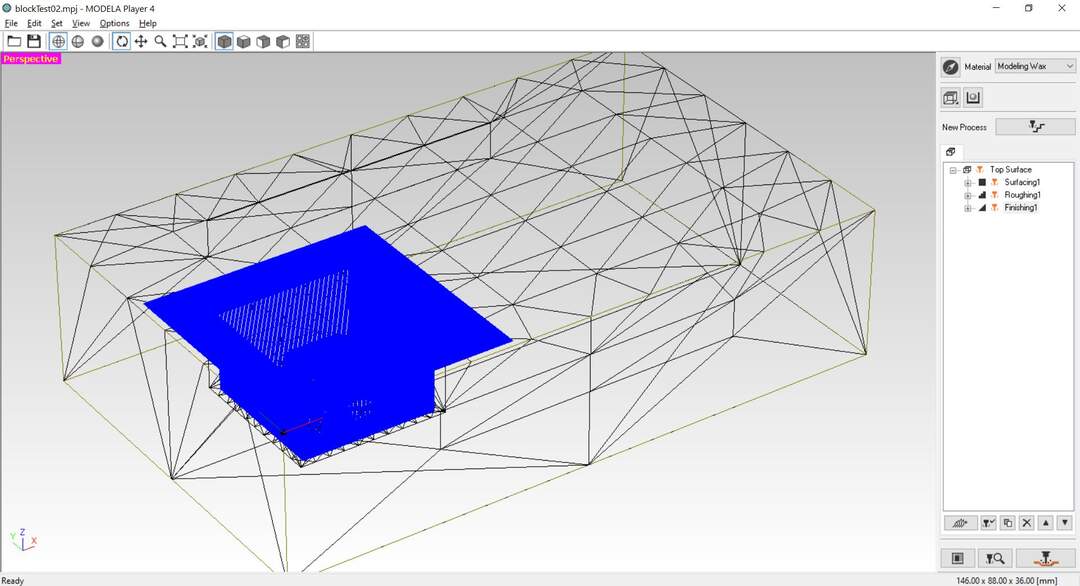
After preparing the 3D file, for generating the machine G-code I have used Modela player 4 which is main software provided by Roland. The alternative for this is to use Fab-module or mod that has pre-define functions for this task. the process in Modela is starting by defining the stock and the origin point according to the material. After that I set the material type which will be used for feeding rate and speed of the machine. After doing these process I make the tool that I wanted to use and calculate the feed rate and speeds according to the material (automatically done by software just needs to be imported to the tool setup). The first strategy will be surfing the bricks since they are not perfectly flat. I should mention these wax are recycled in the lab and does not have perfect leveling at the top. I went 3 mm down to make sure all area around my mold is flat. After leveling the top part of the brick, the roughing strategy will take palace. I have used roughing in just x direction just to save some time and because the shape was not so complicated. For finishing I have used the same milling bit in the x and y direction with 20% over stepping to reach a smooth finishing. One of the challenging part of this model is the really thin pins. I was worry if they gonna coming out well but. it came out perfect.

Running the SRM-20 for milling mold
After generating the files, I start setting up the material and milling bit on the machine. For attaching the wax brick to the sacrifice board I used double sided tape. Make sure the surfaces are all clean to avoid any error. I have used 1/8 inch milling bit for my files so mounting it on the spindle. Then moving the machine in x and y axes to set the zero pint same as the one we set up earlier in the software. for setting the Z I just untighten the milling bit and let it drop slowly on the wax. In order to be able to use this trick you have to let a bit of space for z axes movements. And also some length of bit inside the collet to make sure it would not come off the spindle. Then I just hit the run button and check if the machine does it suppose to. Start with surfing, roughing and finish up with finishing file. Remember that when you do the surfing at the beginning you do not need to re set the z value. It already has been considered in the software while you prepare the files.
Casting silicon

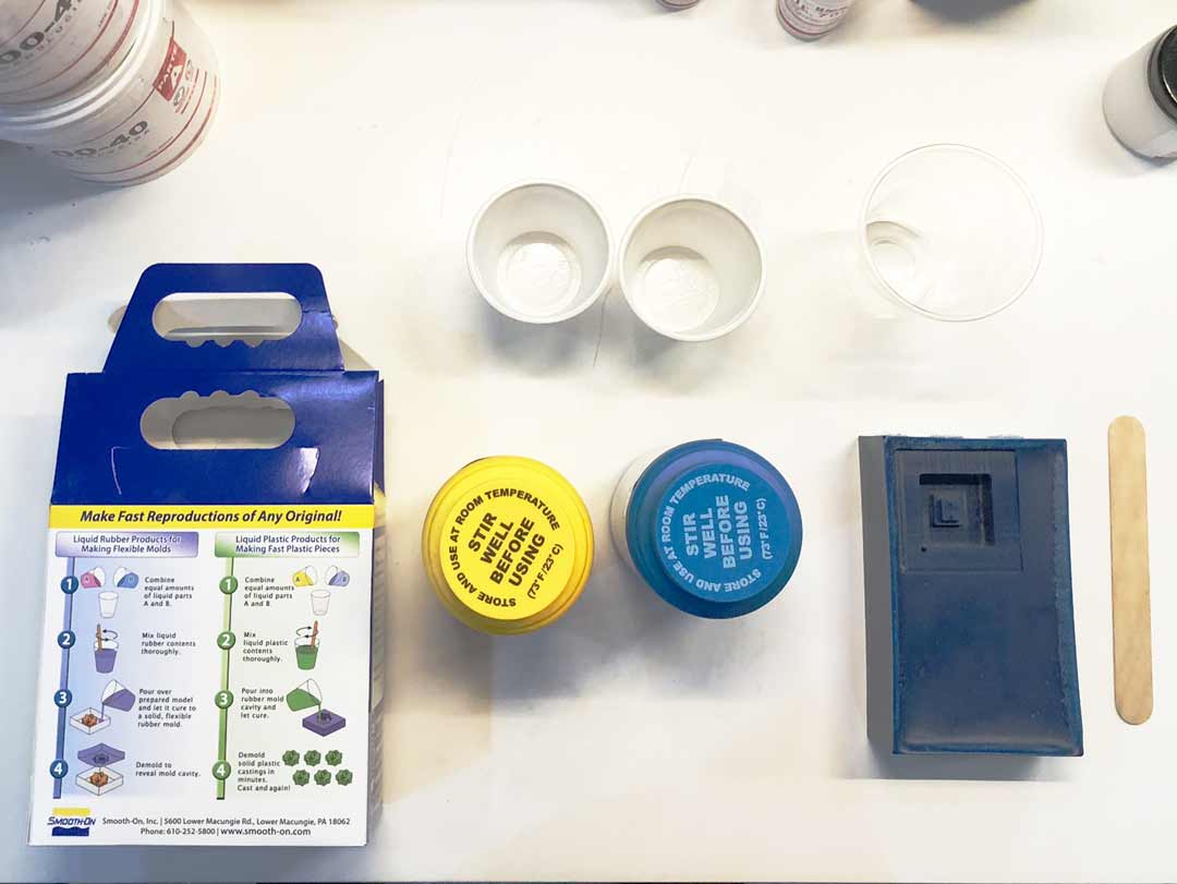
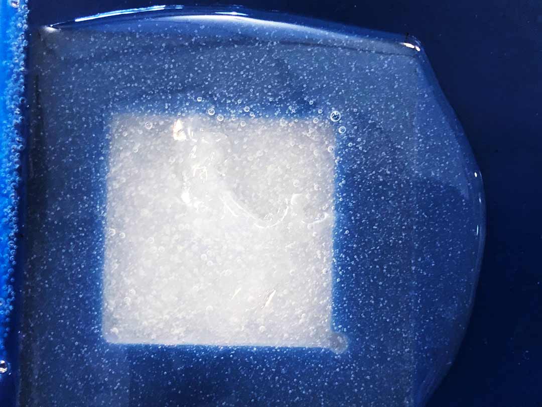
Casting resin
For resin casting I used uv cure resin epoxy. The important thing that you should consider when working with this material is to have a gas mask. Also be aware that this material is highly flammable. For taking the material I used a syringe since I did not need very large volume of it. for this process I also added an acrylic base for the mold to make sure the resistor will be straight in the mold during the cast. After finishing the casting, I left the mold for a 35 min in the front of direct sun and then for 20 mean in the UVB chamber.
Electronic production
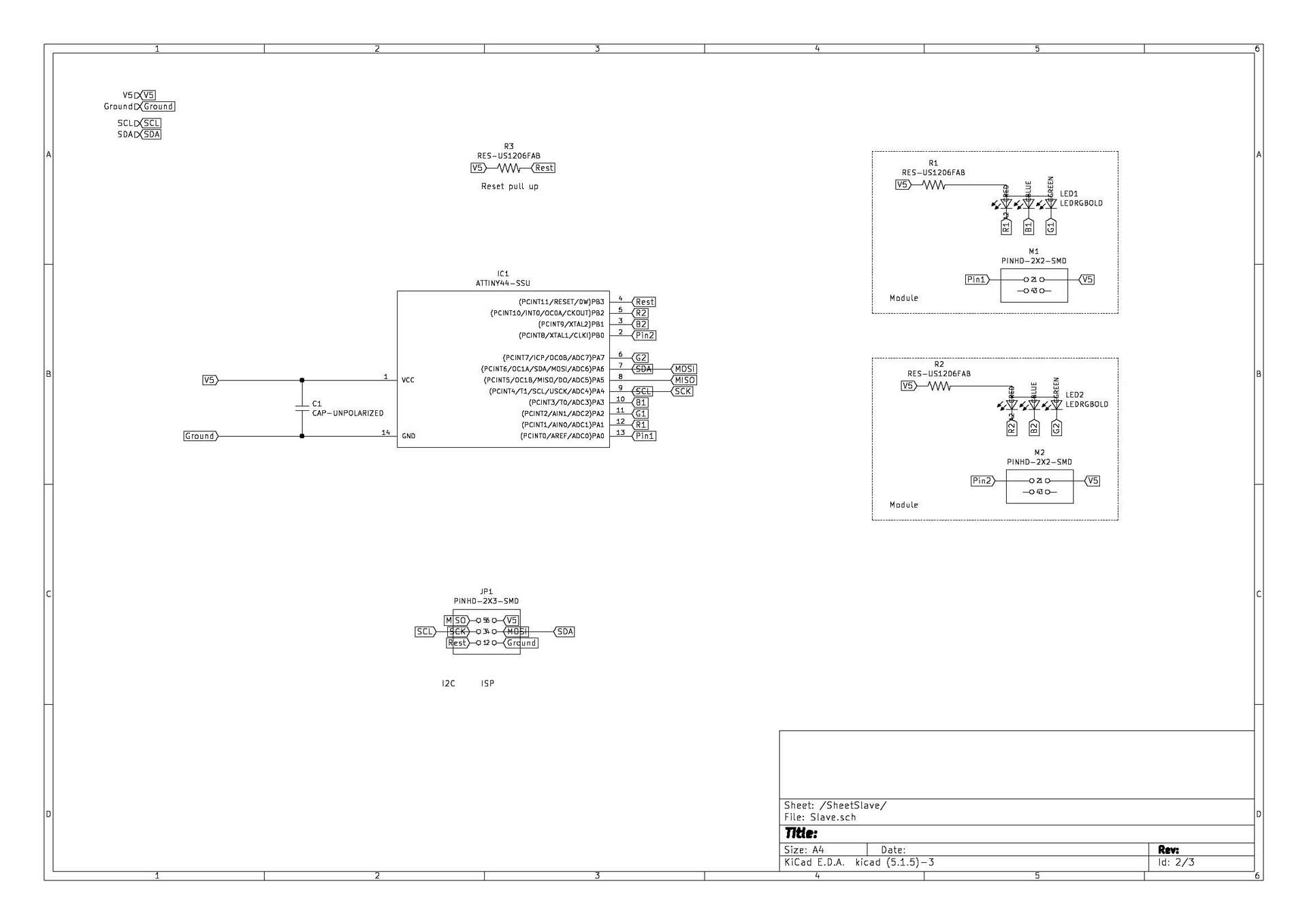
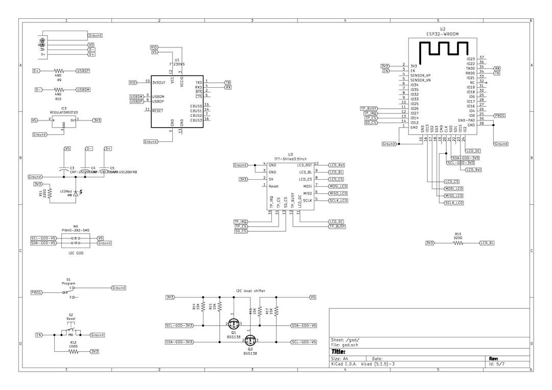
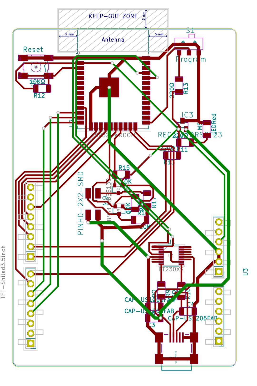
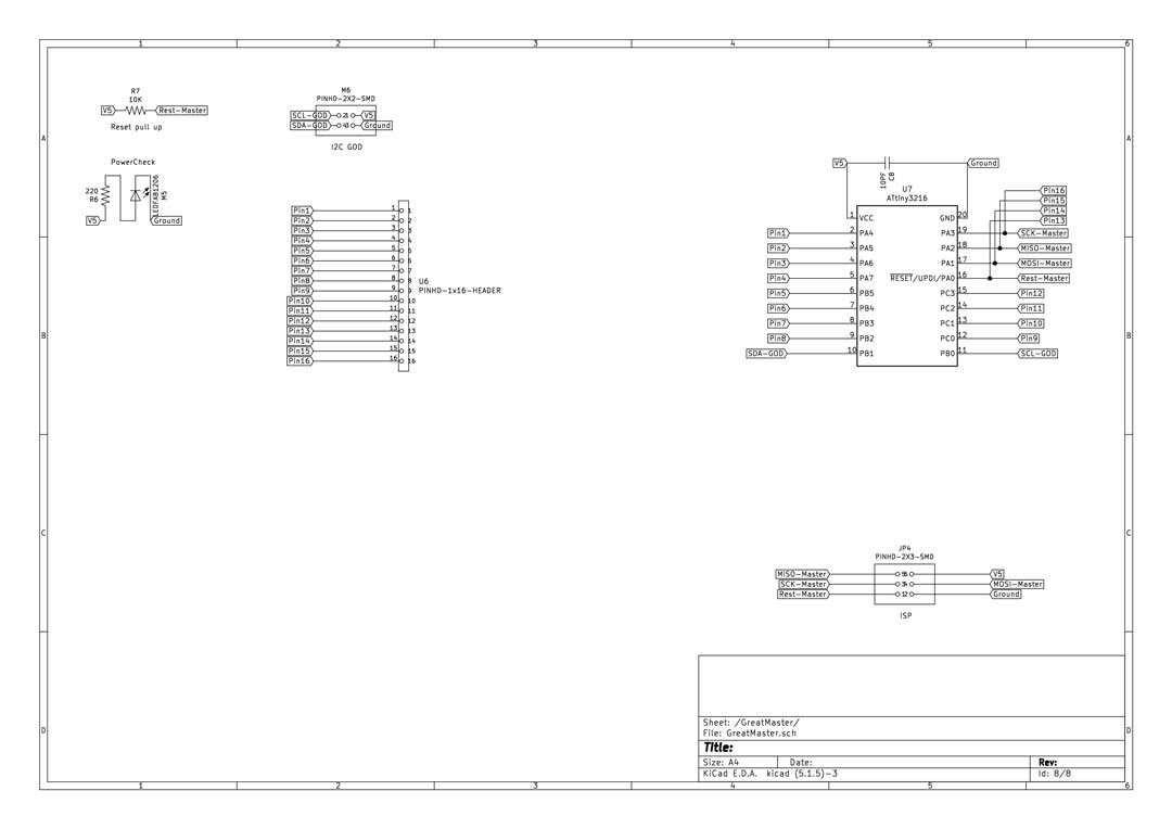
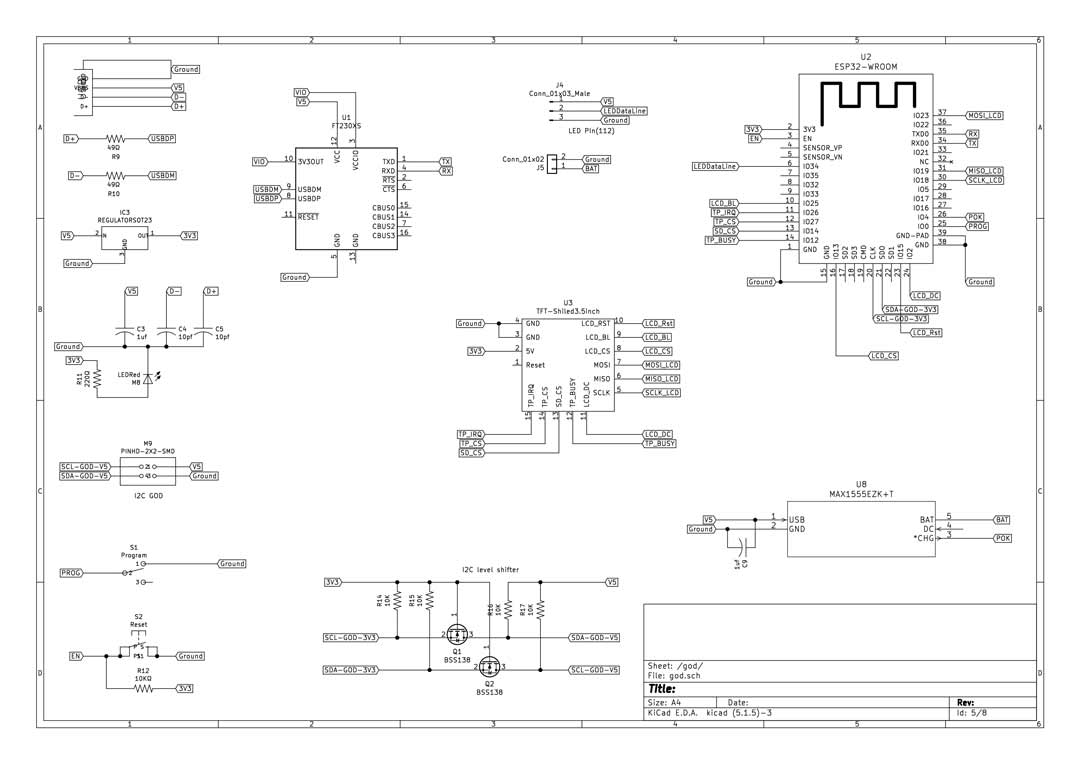
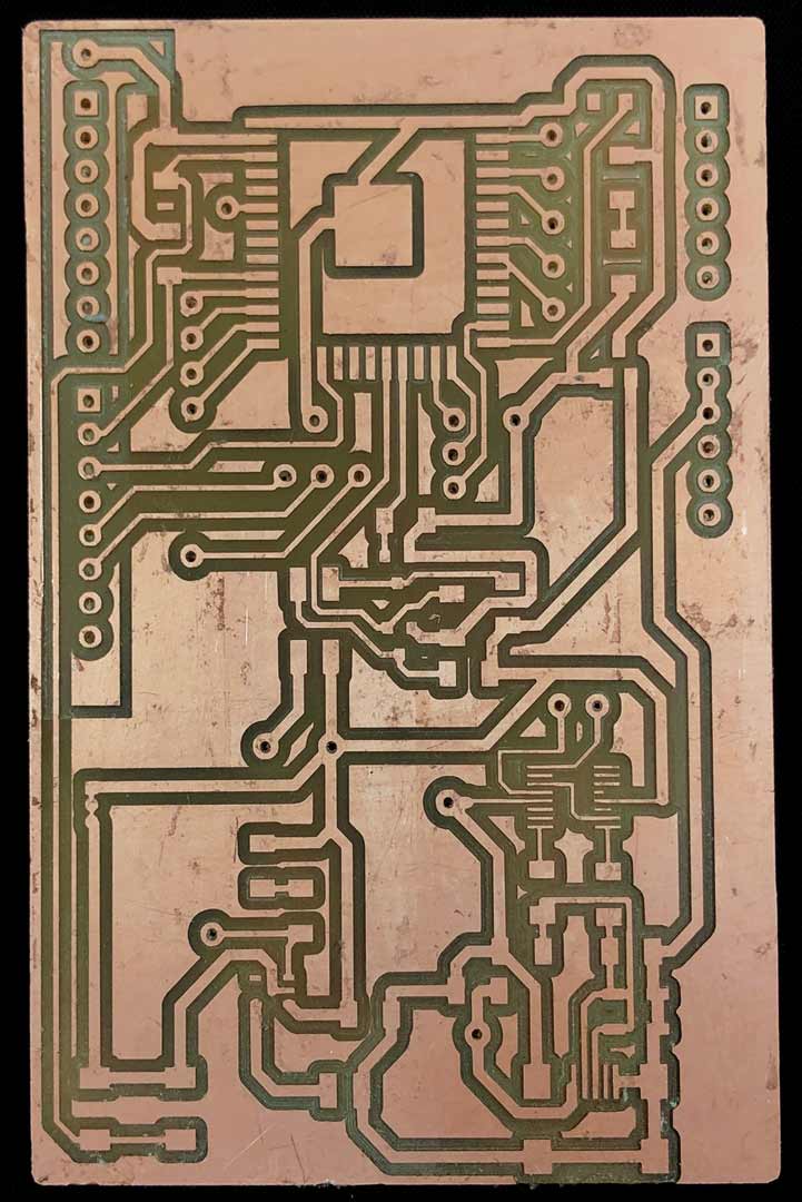
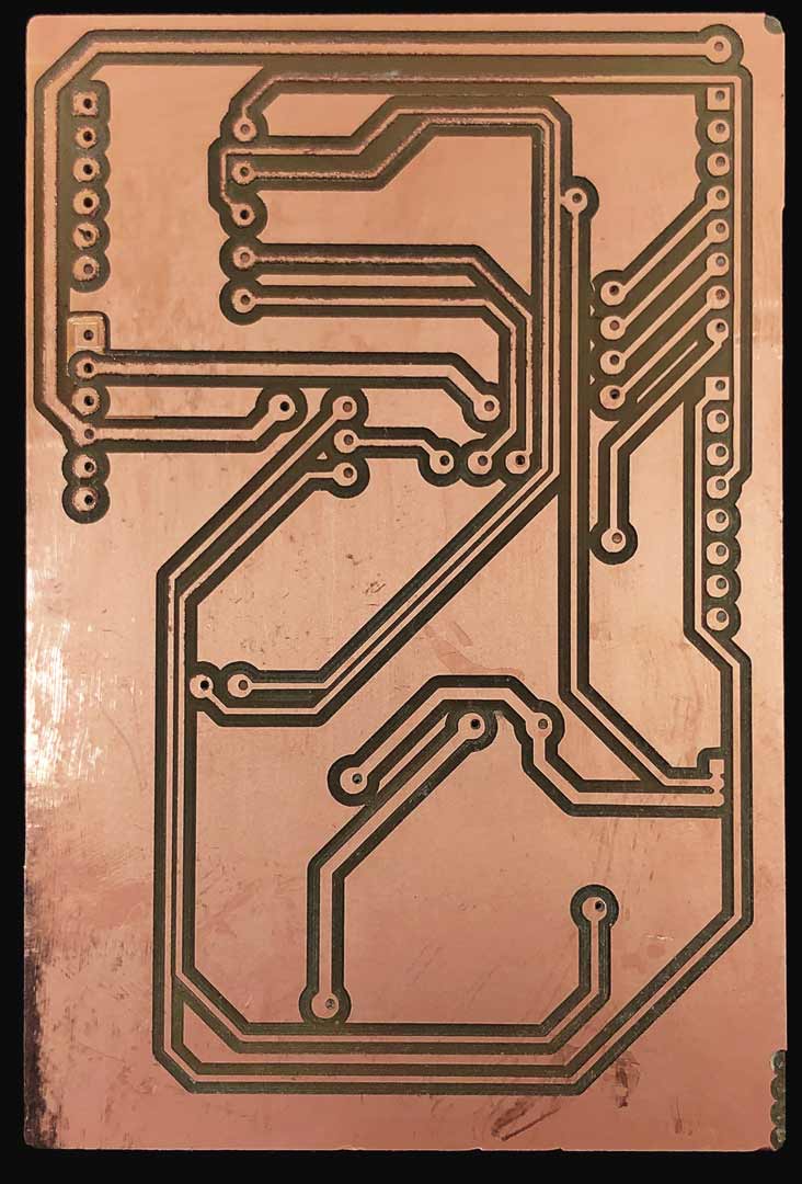
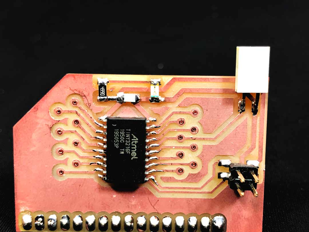
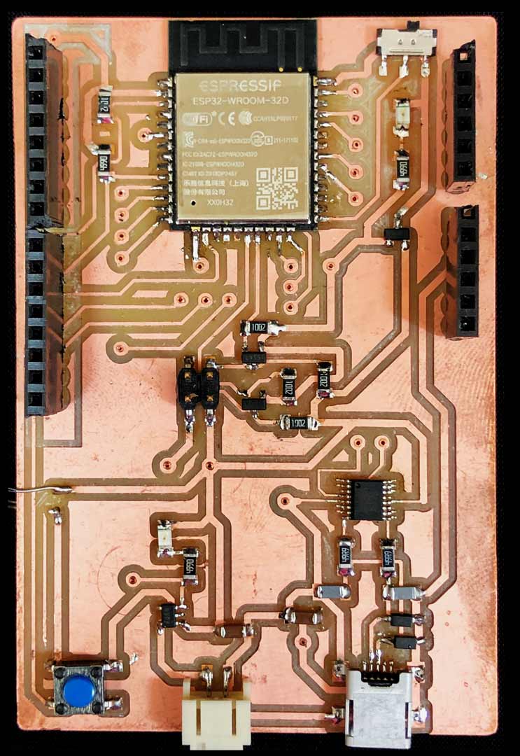
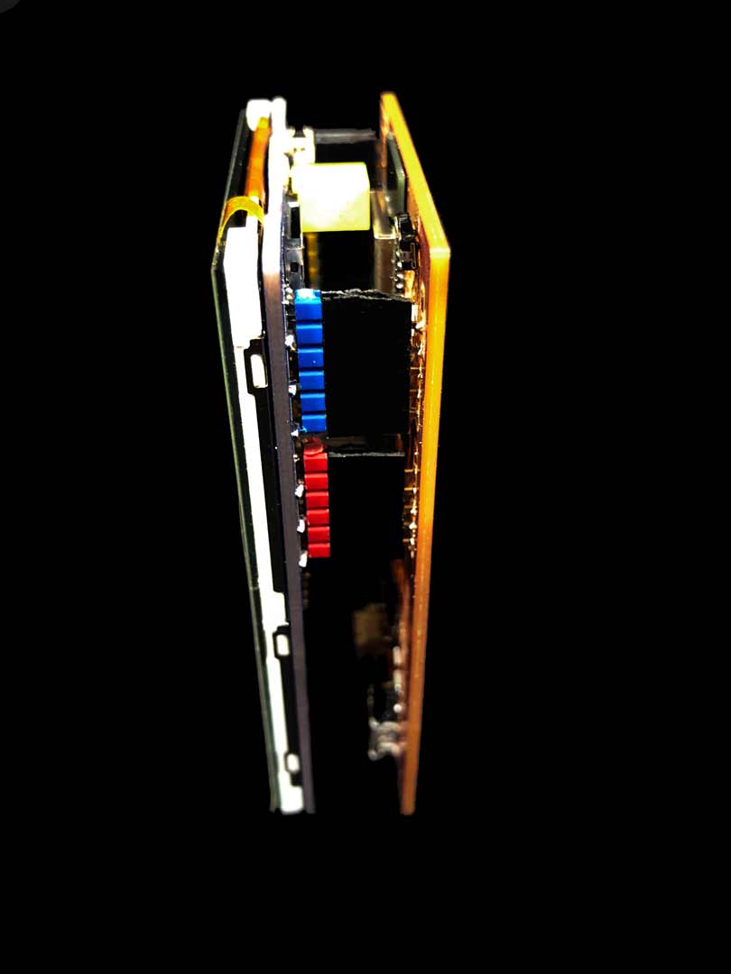
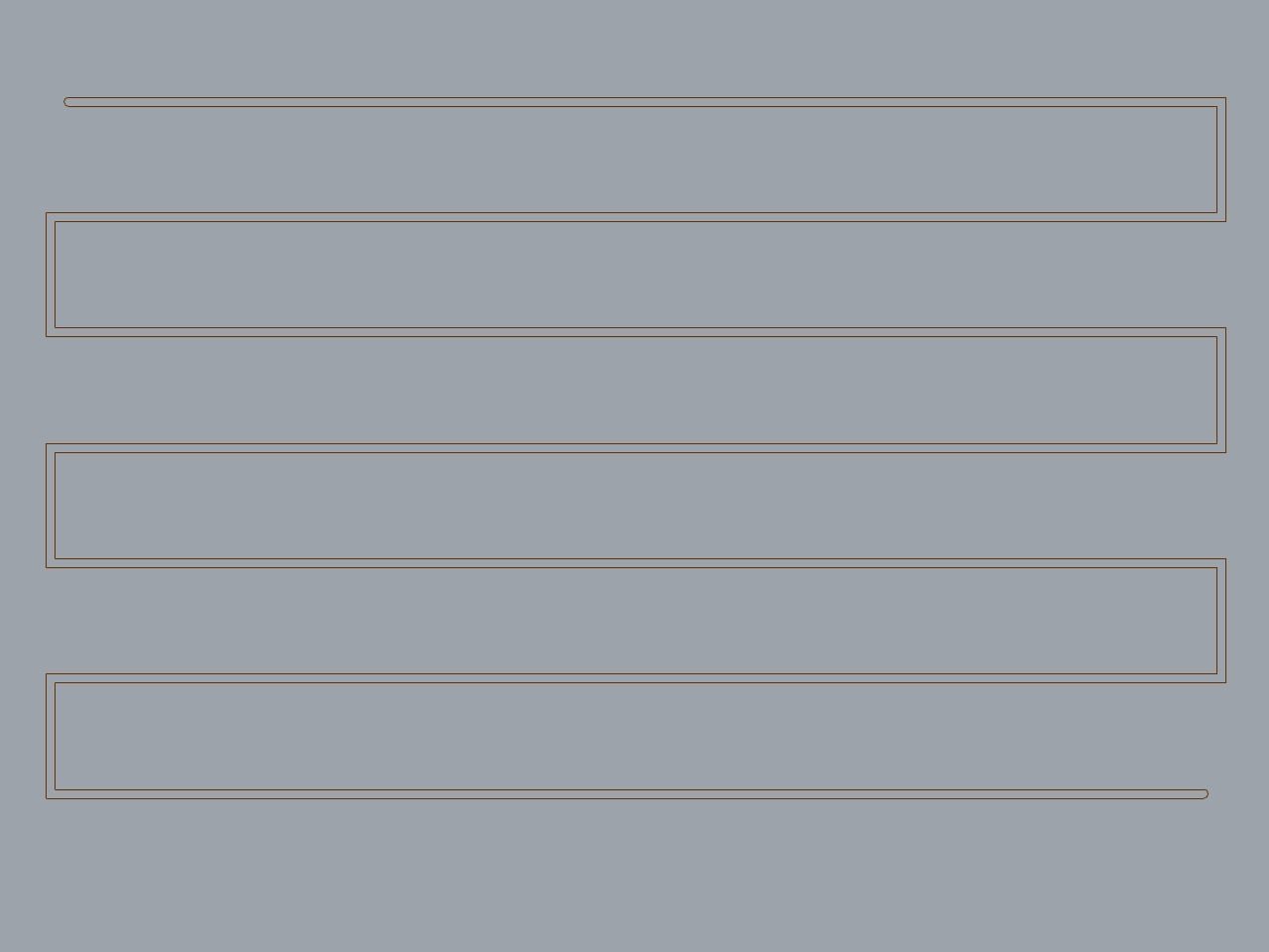
This process is the one that I love the most and I know the least about it. So I start prepare for it much earlier then any other process just to consider some times for error correction. I made some schematic base on what I found in class links and what I found on datasheets of components. Through 2-3 pin-pong consultations with my instructors we went through various range of possibilities of strategies to achieve what I had in mind. To make this a bit clear I am going to explain the architecture. The challenge of my electronic architecture was to have 16-24 IO pin to receive data. At the beginning I was using I was using a lot of attiny44 board which they could address to 2 pins and handle LEDs locally. The good thing was that I had smartness in the low level but the question was do I need this ? and also can I produce 80+ board? and if I did so can I fit them in this tiny space that I have? After discarding this my instructor told me that I can extend the pin numbers on any device by using shift register which basically is a logic memory. I redesign my system base on this component and try to find some example online about how to PWM read this pins. I found that it possible with some trick to write PWM on this pins but not vice versa. After this dead end track, we start to think about a bout Attiny3216 which does have 16 pin out. I did use this chip and redesign my slave part. In the master part story was different the chip and the architecture was clear but I needed to adopt and manage the different part on it. It was ESP32 chip with a ftdi chip, battery charger , level shifter for I2C lines, output line and power for LEDs, and at the end it has to host a TFT shield which was originally designed for Arduino UNO. One of the confusing part of working with ESP32 for me was the pins number. There were different source some base on dev board not the chip and some base on the chip but not pin out code. Long story short, I have messed up so many part of this design and I manage to make it work partially.
First mistake was using wrong regulator. I was using a regulator for small Ampere (10 mA) how every I needed 10 times more power to run ESP32. After so many trouble I manage to change the component. After that I realized that I have IO pins that are connected to internal ISP. the problem was from those different references for pin numbers. So Instead of using IO22 and IO21 I was using pin number 22 and 21 which was completely wrong. The other stupid mistake that I have done was the using wrong footprint for LED terminal. Also realized that the fast LED library is not working with all of the pins of ESP32. thus I needed some adjustment there as well. At the end I found out that I have short on my tft shield terminal which burned the shield completely. I think I went wrong in any way that was possible. Happy did all the mistake so I do not have any excuse for the next gen of this board.
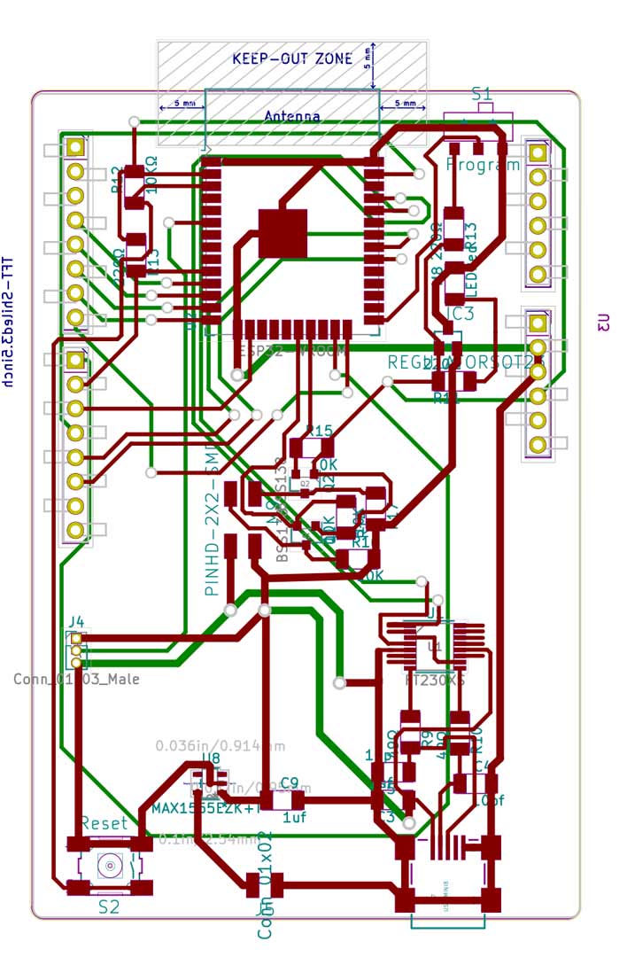
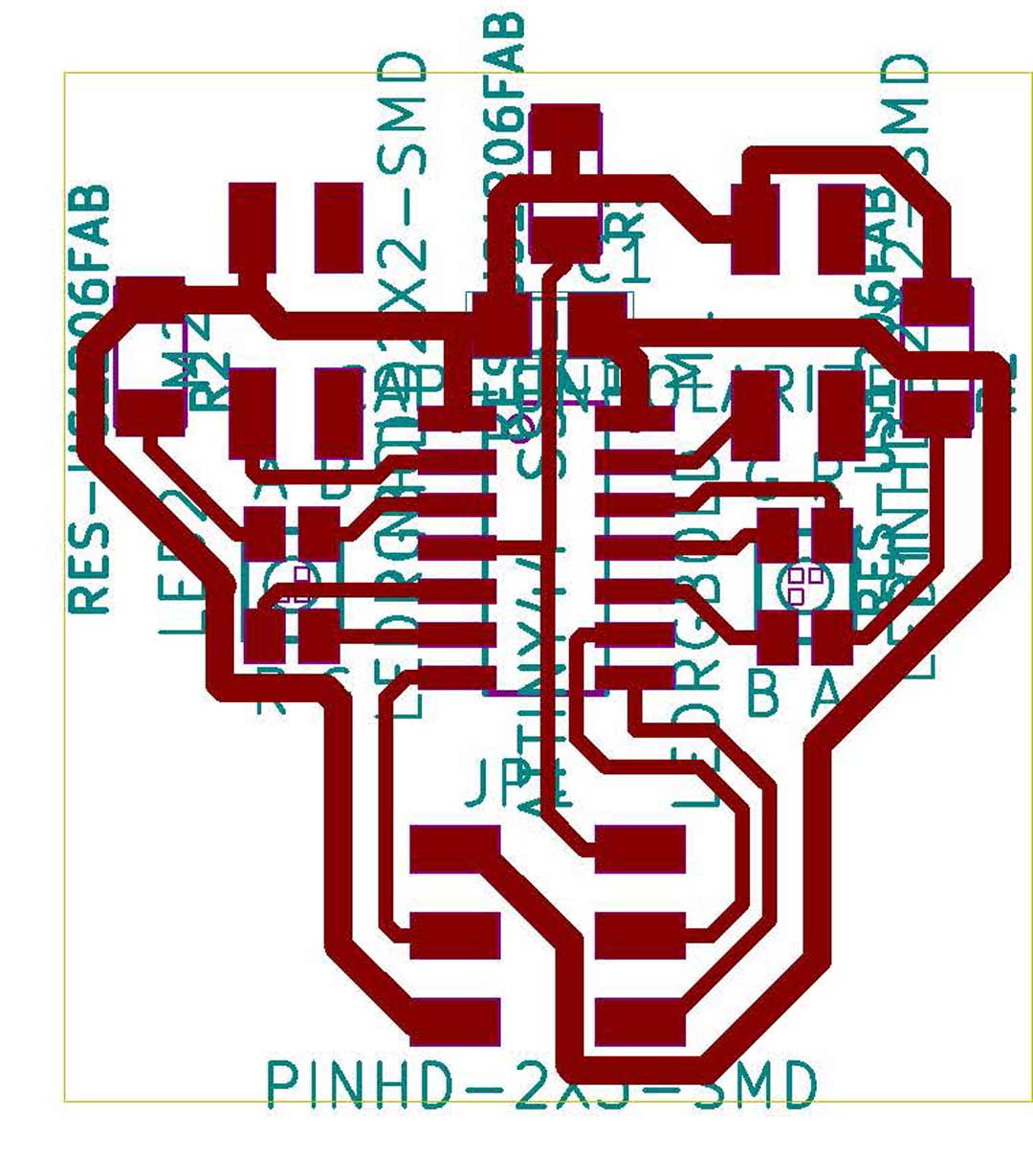
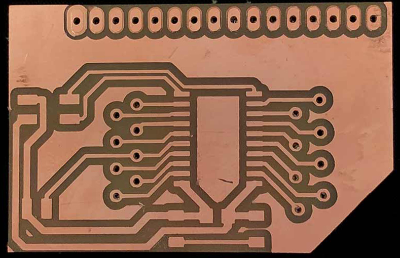
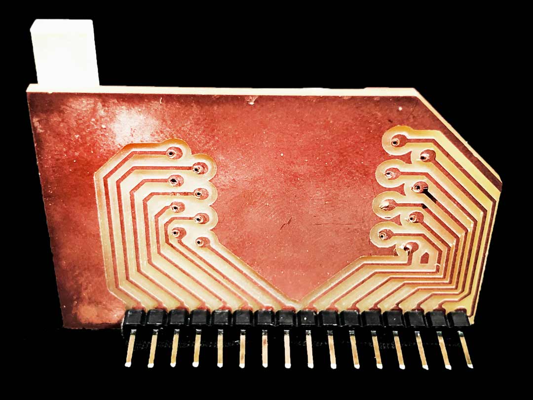
double side PCB Technique
One of the think that I was really keen to push was double side PCB production which we did not have chance to try earlier in the course. So the trick was to first do the holes and out line. after making sure that the pcb still stick to the board. changing the milling bit to do the front face traces. Key point on changing the milling bit, keep the zero for x and y and just change the z (coming from costly experience). When the top face is done take out the cut part gently and clean it. make sure you are not removing any stick with the pcb. Also Remember the direction of the board while removing it because we are just filliping it in one axes. after placing the pcb in its position we can start cutting the trace of the back part. In some case you may need to adjust the Z to make sure that traces are perfectly isolating from rest of the pcb.
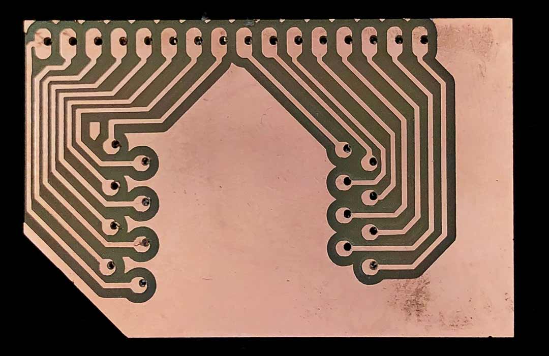
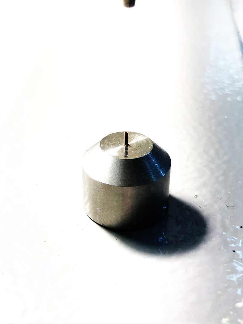
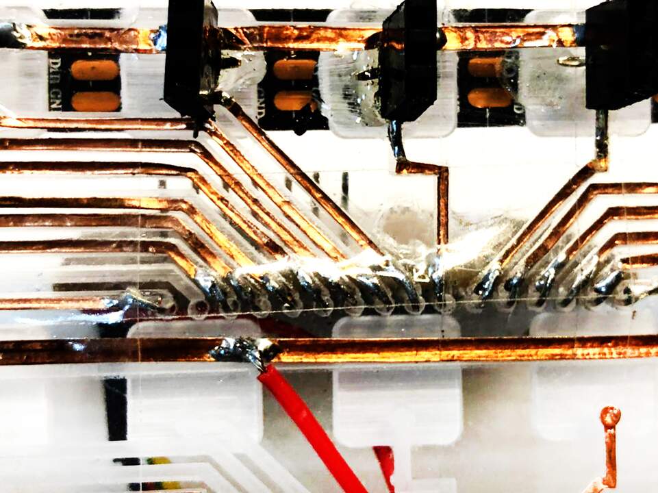
Via installation
This was one of the calming process of all in my whole production. The process is totally manual and needs very steady hand and a lot of patients. Brief explanation that Via is the really small cupper tube with the flat bottom which let it to hoke inside of the holes. And it has been used to connect 2 side of the pcb. The process is simple put the via in the hole, place the hole on the very small nail, punch the via to the pcb. However giving the fact that the size of this elements extremely small make this process very challenging. My trick for this process was to place the via on top of the nail instead of putting it inside the hole. Thus I had better control and visual on position that I have to put the via in. If you catch the knish it would be very fun process. I personally enjoyed it a lot.
Soldering
The most challenging component to solder in my design was ESP32 and FT230xs because both has relatively small footprint legs. With the FT230xs the trick was to connect all the legs and then clean and reflow with the cupper cleaner tape. Also don’t forget to check the position and direction before soldering. In case of ESP32 first problem was the first connection. It was very slippery and hard to keep it aligned in position. My Technique was to add solder on ground pins on the board so I could increase the friction a bit and then reflow on them to make sure the chip is fixed on the board. for soldering the rest of the pins, I have tried to keep the tip of soldering iron on the trace under the chip and heating it for a second. Then I added solder on top and pull it over the trace.
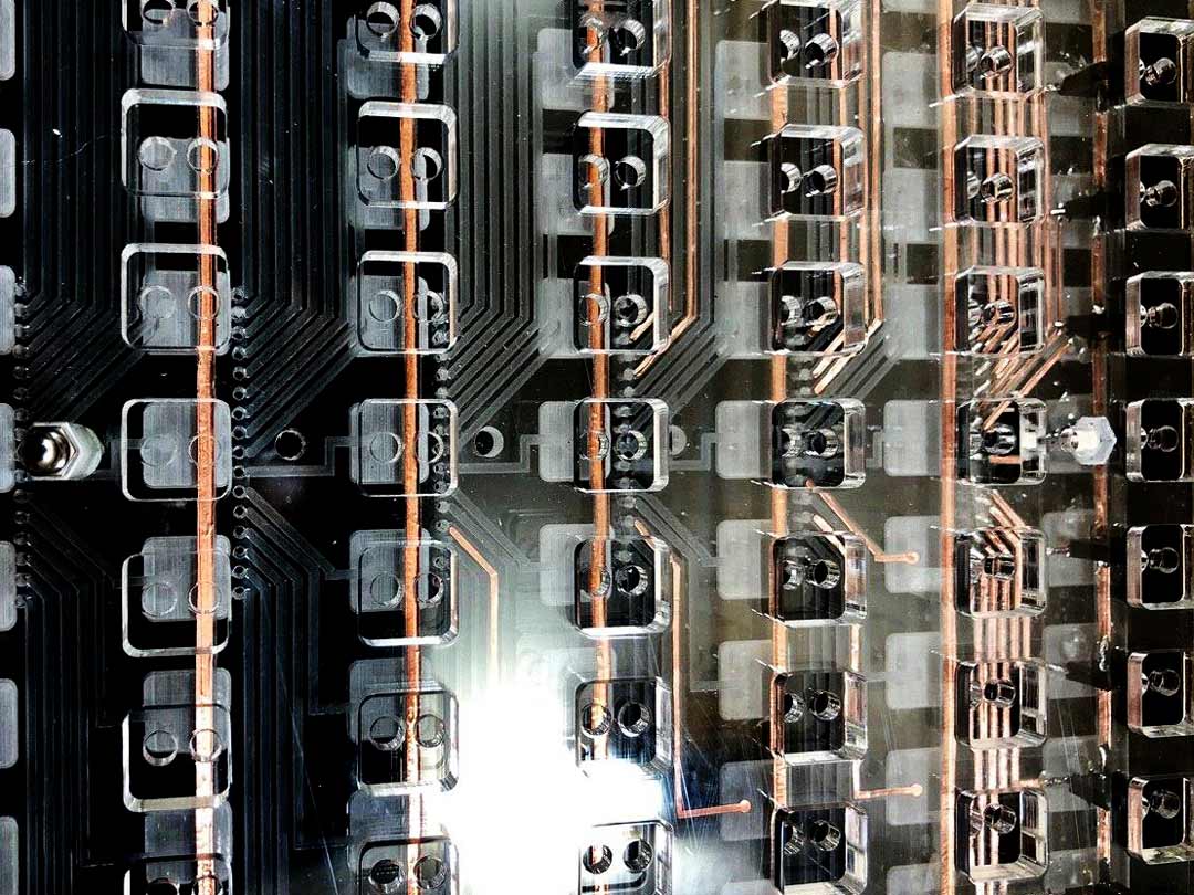
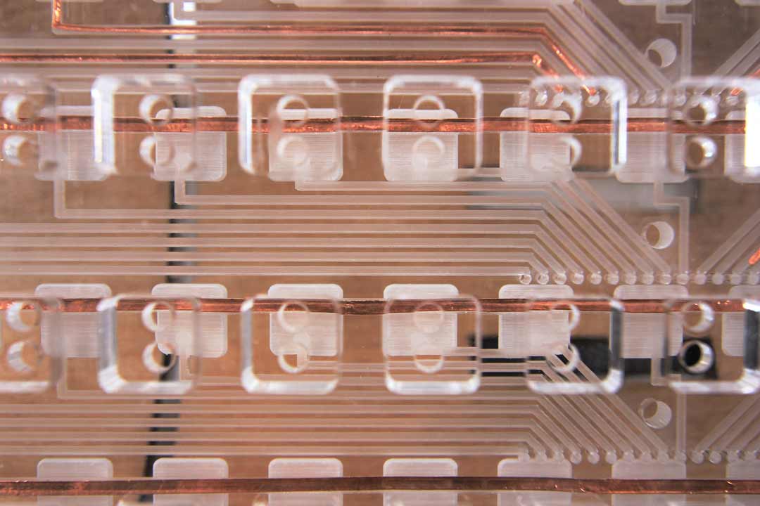
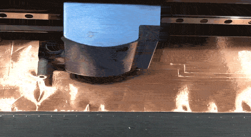
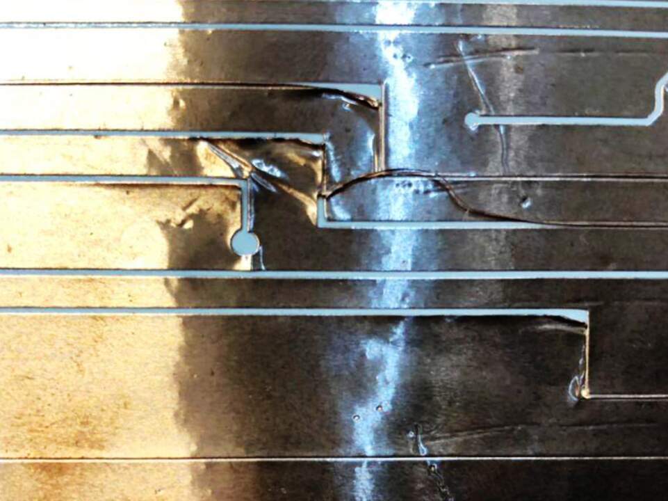
Laser and vinyl cutting
Most of my project has been made by laser cutting method, thus I tried to push it beyond what we learned in the class. In the other hand I really wanted to try making a transparent circuit for my project. Although it was very challenging and it didn’t work as I had imagined it but I am happy with the experiment and in some extend with final result. The most hardest part was how to cut and transfer the copper traces which were cut vinyl cutter on to the acrylic sheet.
Profiling with laser cutting
To use this technique, I design the out line of the profiling section. then I hatched it solid black so it makes a solid raster area. In the laser cut setting I set to engrave those areas but I had to do it in multiple layers. After testing I found out that each 3 time engraving will remove 1 mm of the acrylic. So I start moving the laser 1mm down each 3 times. In total I have removed 2.5 mm. The important tip is to remove the protect plastic from acrylic cause it will melt and burn during engraving.
double side laser cutting
I wanted to try this and see how it will work. I start by sending the back part of the design which was a raster. in the next step I cut the boundary of my design. After that, without moving the stock I flipped the piece. For cutting the other side I had to mirror the design of it with same axes that I flipped the piece. After couple of the cuts I could say that everything is in place. One of the mistakes that I did during this processes was forgetting to fix acrylic sheet to the bed so it increase the chances of the error during the flipping.
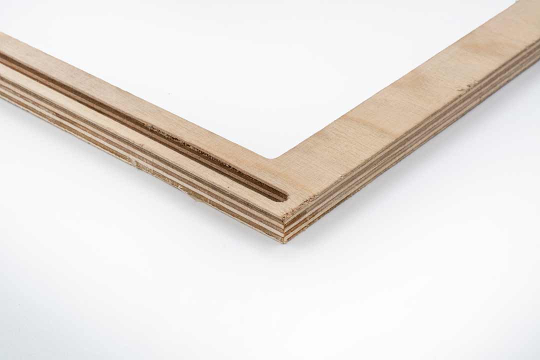
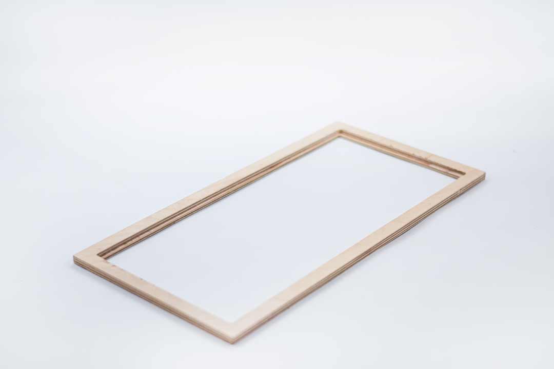
Laser cut bendable plywood
It was very interesting material but very hard to laser it. assuming because of certain binding materials. For preparing the file I had to unroll the designed object to a flat design which will give me the shape after bending. Also I had to consider a margin for the length of the plywood after bending which caused by fiber compression in the wood. After preparation of the file, I have cut it with some trouble. I needed to use more power to make sure it is going through the material which made some smoky part in the plywood. Also it was very hard to keep the material flat on the laser cutter bed. Then I socked the piece inside water for 24 hours. After it became more flexible, I bended and clamped it to the frame. It took 16 hours to dry and get the shape.
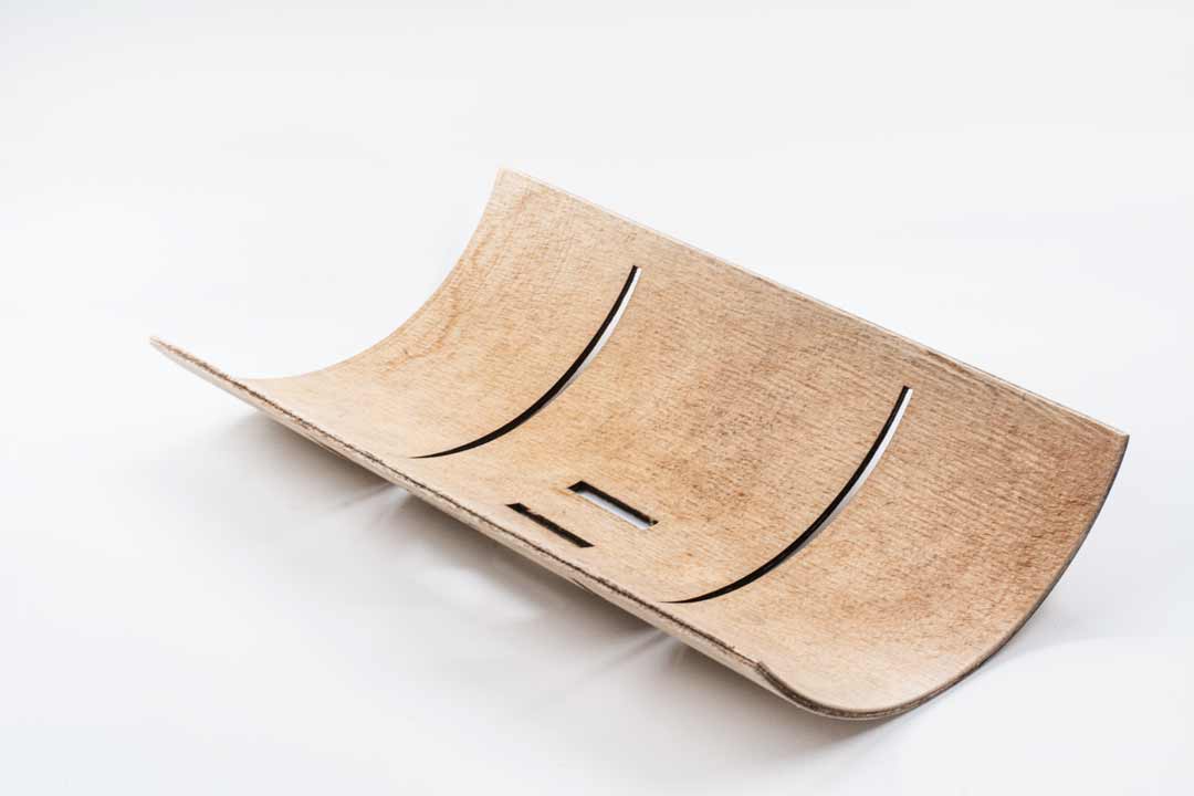
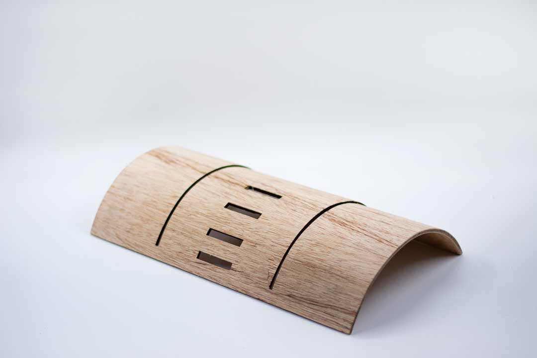
Unfortunately, there is no document before bending the piece.
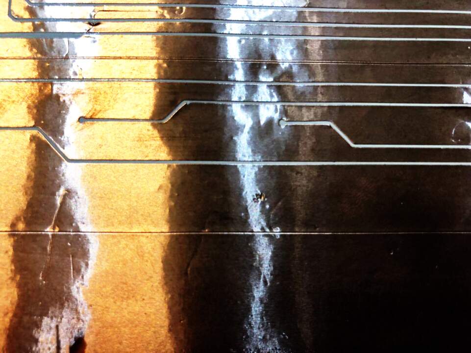
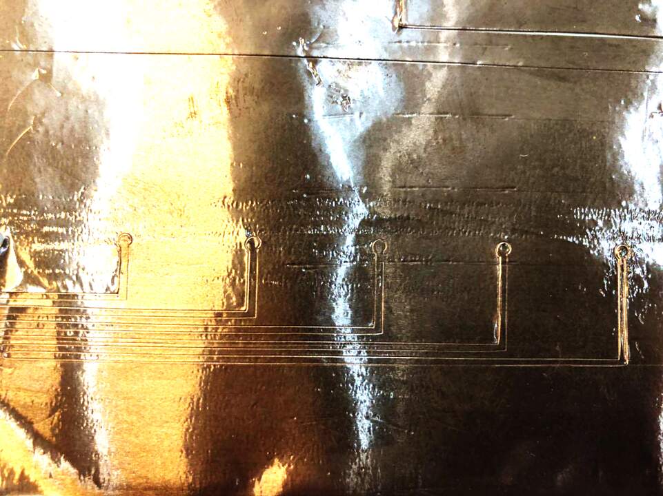
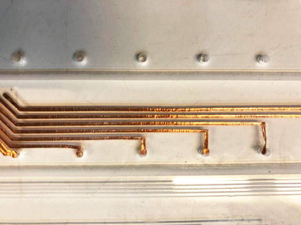
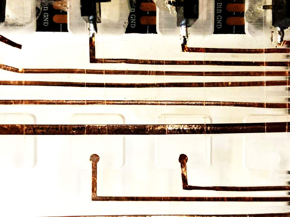
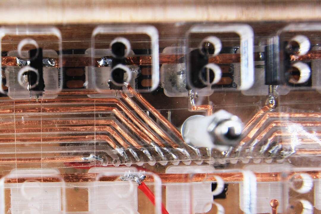
Copper vinyl Cutting
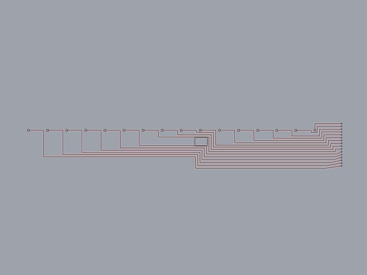
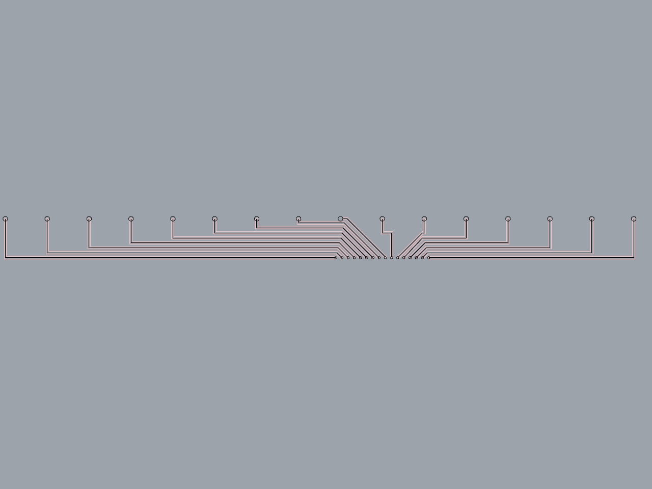
In order to integrate the circuit in the laser cut pieces of acrylic, I have used copper vinyl. First I design the path of the copper on rhino (not kicad although I could do that but it needed extra steps as I needed to add my slave board as a component to project library). Like pcb design I have considered the thickness of the traces to be around 0.4mm (BIG MISTAKE). Then I went on Roland vinyl cutter CAMM-1 and start testing to find the best force and speed for cutting the copper. I tuned it on 140g force and 10cm/s speed. The result was very bad and I had to stop the machine because the traces were coming out and sticking to the needle of the cutter. I have realized that the area of the trace need to be larger to stick to the vinyl before transferring it. Back to the design face, I needed to increase the thickness of the traces up to 1mm but I did not have enough space to do that. Thus I ended up rearranging the whole layout for traces. In this new layout I had to plug my pcb in the back of the board therefor I had to make holes for the pcb pins to be inserted. after couple of fail attempts I start produce them in mass volume and tack the best one from each series. After stick them to the board and fill one day of the week, I faced another challenge. the pin legs was not stable on the trace and there would be a lot of noise in reading. So I decided to solder female terminal on the traces. The problem was that whenever I apply the heat to the copper vinyl it was losing its stickiness to the surface. also the temperature should not apply for long other wise it could burn the acrylic. To solve the first problem I used transparent resin glue for the parts that I know it is vulnerable. for the second I did not have any solution rather than doing it fast.

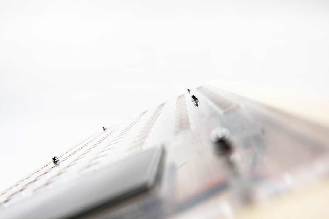
CNC Milling
I have used cnc milling to fabricate the frame of my project. The strategies that have been used are engraving, pocketing. Moreover the piece needed to be milled from both side. For this reason, a strategy is profiling 2 holes for 2 metal bars to hold the position of the piece when I flip the stock to do the other side. the first strategy will be the engraving the screws position. Just a good practice to have the position of the screws digital and make sure the milling bits is not gonna heat them. Then there will be a engraving of lines that is going to hold the bended back plate. After that, the back part of the frame is cut which was 4mm deep in to material. In the other side I had to run the screw file again to put the new set of them for this side. At the end it will be a profiling with a depth of 5mm.

//TODO: add video
3D printing
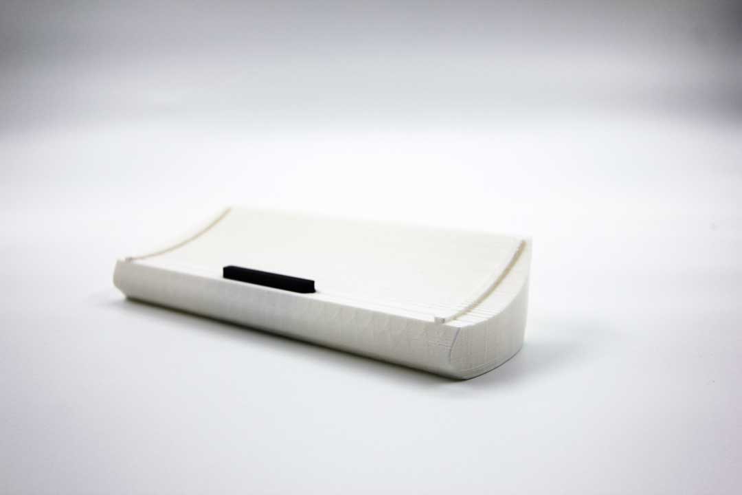
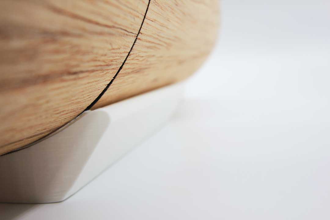
I have used 3D printing technique to make the stand for the panel. The design of this stand happened at the same time with the bended plywood in the for back of the panel. The 3D printed part consist of 2 part. First was the stand which had a rail to fit on the back of the bended plywood. Second part was a pin that act as a mechanism. In my first attempt for printing, The angles that I put the stand to hold the board was very high. So the panel was coming out of the stand. In second iteration, I have adjust the rotation and make the design a bit more smoother to reduce the material usage. The pin was successful in the fist print although it was not functional because of the stand problem at the first iteration. At end the mechanism was not so helpful for adjusting the panel because of the accessibility problem. However it was holding the panel which was it initial purpose. In Following you can find some image and docs from this processes.
Networking
I2C
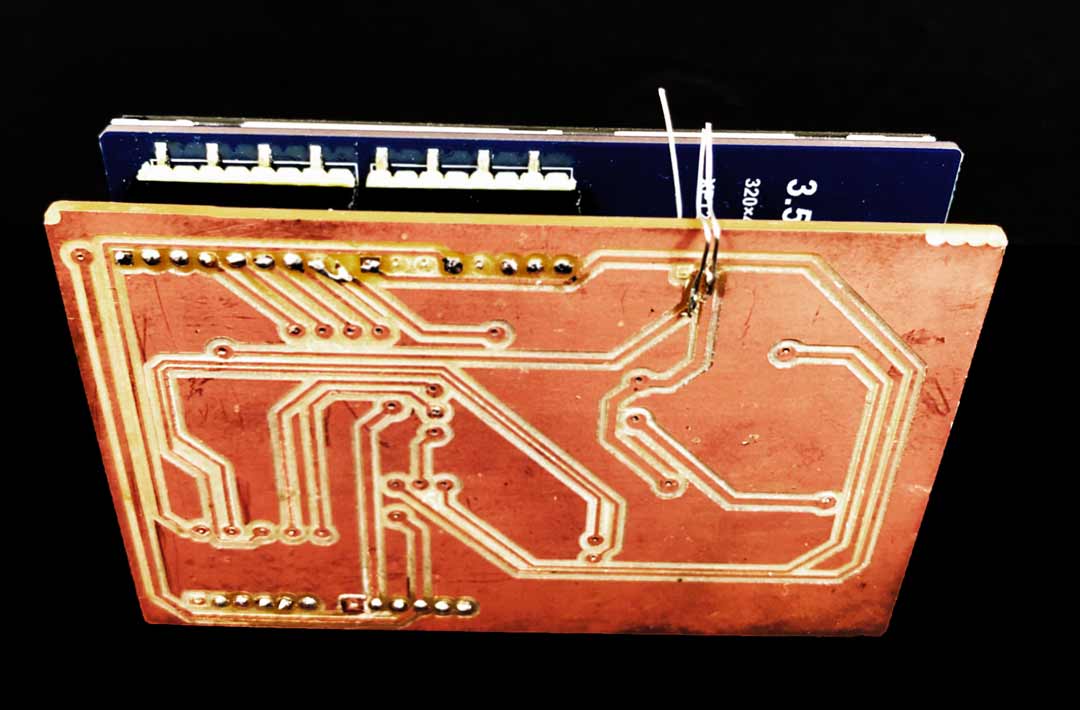
The Networking technique that I have used for communicating between each board in my panel is I2C. As demonstrate earlier in the page. each day of week has a board that detects the input schedule. each of this boards are connected to the motherboard through I2C wire. The technicality that I have to consider at the electronic design stage was the difference between master board and slave boards voltage. To address this issue I had to use a level shifter in the master board to pull the data line to 5V.
For this communication I have implement my own protocols. the bucket that I am sending has 8 bit size and I need to send the value for 9 pins. The value that I needed to send was between 0-4. SO from those 8 bit, I dedicate 3 bit for the value and the 5 other for the pin number. At the end I cast them together and ship them at the master request.
At the master side each 0.5 second it send the request to check if there is any changes. It reads each bit and deconstruct it to the pin number and a int value between 0-4.
internet
In the initial idea of the project, I had in mind to communicate with a web API in order to make this schedule available on google calendar platform. To pull this off I needed to add a client service on the motherboard code to make it possible to send the http request through the web. So I can keep the plan board sync with an online calendar platform. this step has not implemented yet. The problem is mostly the auth2.0 authentication and redirection from node MCU to google page where user can input their credentials. So I have 2 solution to address this issue. either I need to make a middle man like web-App or using Rest to make the communication. The first one is probably easier and safer to do but need an extra server to run.
Embedded programming
I have used pyupdi for programming the slave board which is a Attiny3216. I had some trouble for serial communication for debugging the code. At the end I had to use software Serial and adjust the board to read those pins. The program simply reads the value of the voltage and base on the static resistor that are connected to the pins it calculate the connected resistor in the schedule blocks
master code
// I2C lib
#include <Wire.h>

// FastLED lib
#include "FastLED.h"
#define LED_PIN 16
#define NUM_LEDS 16
#define BRIGHTNESS  64
#define LED_TYPE    WS2811
#define COLOR_ORDER GRB
// Communication var

byte pin;
byte st;
byte sch[2] = {0b001, 0b010};
bool check = false;

// LED var
CRGB leds[NUM_LEDS];


void setup() {
  Wire.begin();  // join i2c bus (address optional for master)
  Serial.begin(115200);  // start serial for output
  Serial.println("hello esp32");
  LEDSetup();
}

void loop() {
  BaordUpdate();
  delay(500);
}

void BaordUpdate() {

  ////////////////////////////////commuincation///////////////////////////
  byte c;

  //int count = 0;
  Wire.requestFrom(1, 9);    // request 9 bytes from slave device #1
  Serial.println("req sent");
  while (Wire.available()) {
    Serial.println("wire is available");
    c = Wire.read();
    ConvertToid(c, &pin, &st);
    Serial.println(c, BIN);
    Serial.println(pin);
    Serial.println(st);
    //count++;
    //Serial.println(String(count));
    /////////////////////////////////////////////////////////////////////////
    /////////////////////////////////LED management/////////////////////////
    ////////////////////////////////////////////////////////////////////////
    if ( pin > 6){
      pin = pin -1;
    }
    LEDColor(pin , st);
    FastLED.show();
    FastLED.delay(20);

  }


}
void ConvertToid(byte c , byte *pin , byte *st) {
  *pin = c >> 3 ;
  *st = c & 0x07;
  /*if ( tep == sch[0]) {
     st = 1;
    }
    else if ( tep == sch [1]) {
     st = 2;
    }*/
}

void LEDSetup() {
  FastLED.addLeds<LED_TYPE, LED_PIN, COLOR_ORDER>(leds, NUM_LEDS).setCorrection( TypicalLEDStrip );
  FastLED.setBrightness(  BRIGHTNESS );
  leds[0] = CRGB::Red;
  FastLED.show();
  delay(500);
  // Now turn the LED off, then pause
  leds[0] = CRGB::Black;
  FastLED.show();
  delay(500);

}
void LEDColor(int pin , byte st) {
  int num = (byte) st;
  int ads = (byte) pin;
  if ( num == 1) {
    leds[ads] = CRGB(200, 0, 0);
    FastLED.show();
  }
  else if ( num == 2) {
    leds[ads] = CRGB(0, 150, 200);
    FastLED.show();
  }
  else {
    leds[ads] = CRGB::Gray;
    FastLED.show();
  }
}
Slave Code
//#include <SoftwareSerial.h>
#include <Wire.h>
#define SDA 8
#define SCL 9

/*const byte rxPin = 8;
  const byte txPin = 9;
  SoftwareSerial mySerial (rxPin, txPin);*/

int address = 1;
int pin[9] = {0, 1, 2, 3, 4, 5, 14, 15, 16};
int digPin[4] = {10, 11, 12, 13};
//int todo[4] = {30, 200, 800 , 1024};
byte tosend[8];
byte sch;
byte buff;
int count = 0;


void setup() {
  for (int i = 0; i < 9; i++) {
    pinMode(pin[i], INPUT);
  }
  for (int i = 0; i < 4; i++) {
    pinMode(digPin[i], INPUT);
  }
  //mySerial.begin(38400);
  //Serial.pins(9,8);
  Serial.begin(115200);
  Serial.println("Serial def");
  Wire.begin(address);
  Wire.onRequest(requestEvent);
}
void loop() {
  /*Serial.println("******");
    for (int i = 0; i < 9; i++) {
    /*if ( i == 8 || i == 9 || i == 6 || i == 7) {
      continue;
      }
    //else {
    //sch = PinRead(pin[i]);
    //Serial.println(sch, BIN);
    //Serial.println(sch, BIN);
    int schInt = (byte) sch;
      if (schInt > 0) {
      count++;
      if ( i % 2 == 0) {
        buff = sch << 4;
      }
      else if (i % 2 != 0) {
        tosend[(i - 1) / 2] = buff ^ sch;
        //Serial.println(tosend[i - 1 / 2], BIN);
        //Serial.println("///////////////");
        if (i == 15) {
          Serial.println(count);
          Serial.println("_____________");
          byte br = (int)count;
          tosend[(i - 1) / 2] = sch ^ br;
          count = 0;
        }
      }
    }*/
}


void requestEvent() {
  //Wire.beginTransmission(address);
  for (int i = 0 ; i < 9 ; i++) {
    sch = PinRead(pin[i]);
    Wire.write(sch);
  }
  //Wire.endTransmission();
}

/*void DigPinRead(int pin) {
  int stat = digitalRead(pin);
  Serial.print(pin);
    Serial.print(" : ");
    Serial.println(stat);
  }*/

byte PinRead(int pin) {
  // read the voltage form pin and map the value to the function
  byte sch;
  int vol = analogRead(pin);
  /*Serial.print(pin);
    Serial.print(" : ");
    Serial.println(vol);*/
  if (vol < 30 ) {
    byte pinByte = (int) pin;
    sch = pinByte << 3 | 0b000;

  }
  if (30 < vol && vol <= 200) {
    byte pinByte = (int) pin;
    sch = pinByte << 3 | 0b001;
  }
  /*else if (todo[1] < vol <= todo[2]) {
    sch = 0b0010;
    //Serial.println(2);
    }*/
  if ( 800 < vol && vol <= 1024) {
    byte pinByte = (int) pin;
    sch = pinByte << 3 | 0b010;
    //Serial.println(3);
  }
  /*else if (todo[3] < vol <= todo[4]) {
    sch = 0b1000;
    //Serial.println(4);
    }*/
  //Serial.println(sch, BIN);
  return sch;
}
Google calendar API
I had this feature idea to keep my schedule in sync with a online platform calendar. Still have not implement it but I really want to add this feature in the future. You can follow the google calendar api document in the following link.