redraw an echo hello-world board, add (at least) a button and LED (with current-limiting resistor) check the design rules, make it, and test it extra credit: simulate its operation
Last week we learned how to make an electronic board printed with a ready-made design, and we also learned how to weld the pieces in the correct place. This week, we will design an electronic board using one of the design programs.
Printed Circuit Board (PCB) is a flat plate used to connect electronic components electrically by welding them on conductive paths, which are engraved from the copper sheet chips on a non-conducting substrate. It is the basis of electronic circuits, it is used in all electronic commercial products and it is not possible to manufacture electronic devices or build practical electronic circuits for devices without printed circuit boards.
 is a scriptable electronic design automation (EDA) application with schematic capture, printed circuit board (PCB) layout, auto-router and computer-aided manufacturing (CAM) features. EAGLE stands for Easily Applicable Graphical Layout Editor
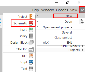
To make a printed electronic board, I will first design the board using Eagle, first we open the program and then we click on open schematics
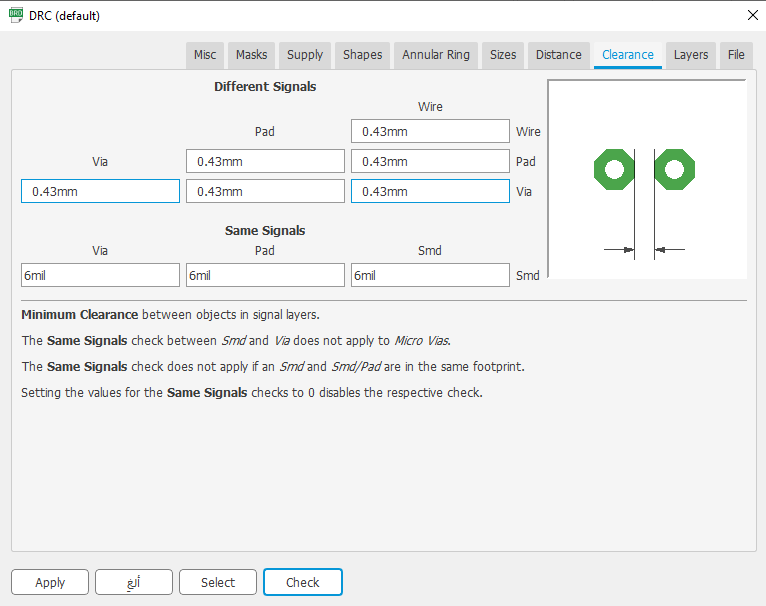
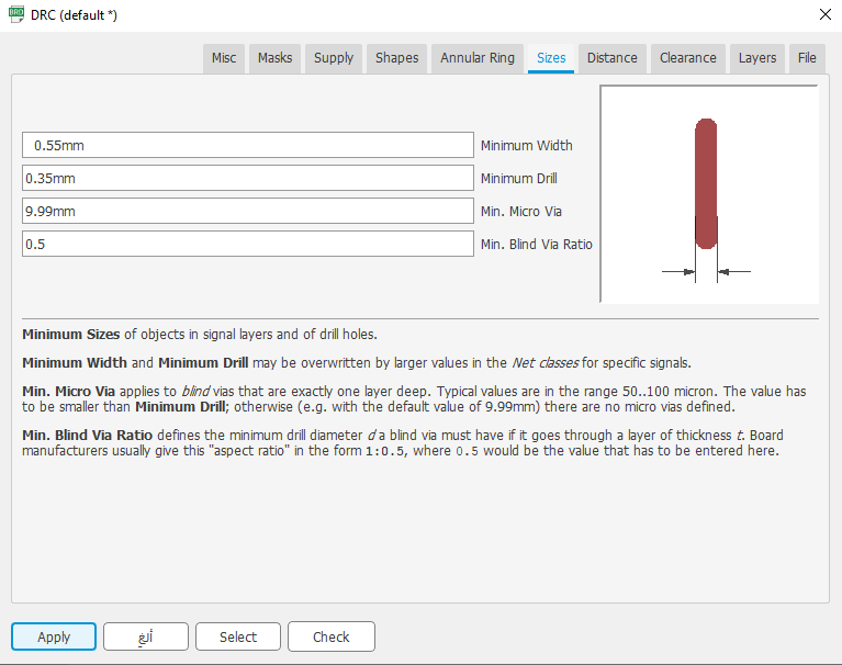
Before starting design I will adjust clarity and volume settings through (DRC)-To start designing with these settings
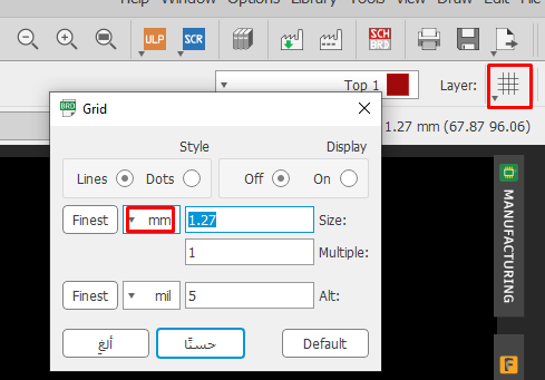
Through the Grid tool, I will change the measuring tool to (MM)
We will be using this week's Atmel Board which is the same thing we used in the Electronics Production Week which was Attiny44. For a good understanding of where I have to connect the components, I checked Attiny44 datasheet.
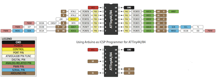
After reading the Attiny44 Data Sheet, I will install these parts:
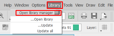
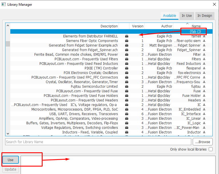
After opening the Eagle program and adjusting the clearance & size settings through (DRC). I will download Fab Library and add it to the program as it is shown in the image below.
 With this command, I will add the things I mentioned earlier
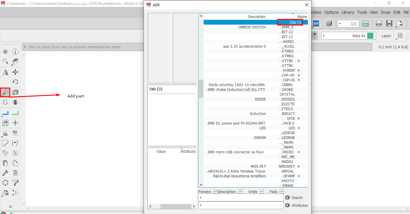
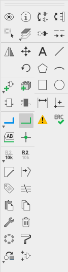
This is a list of tools that we will use a lot in moving, deleting, adding, checking, etc.
After adding all the pieces, I will connect them using a tool
 and I will also name them using a tool
  so that they are connected in place with the rest of the pieces.
When the pieces reach each other by naming them, this message will appear to you
so that they are connected in place with the rest of the pieces.
When the pieces reach each other by naming them, this message will appear to you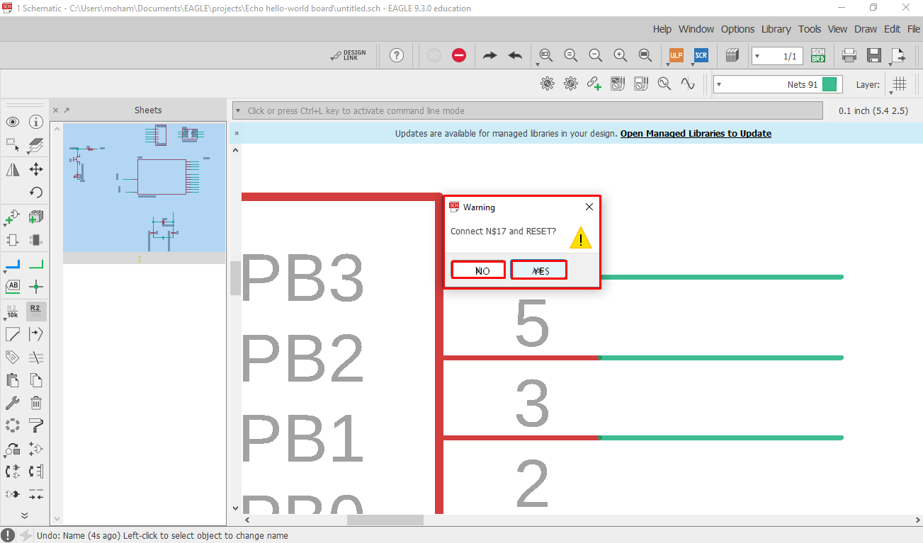
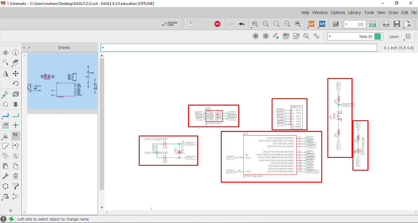
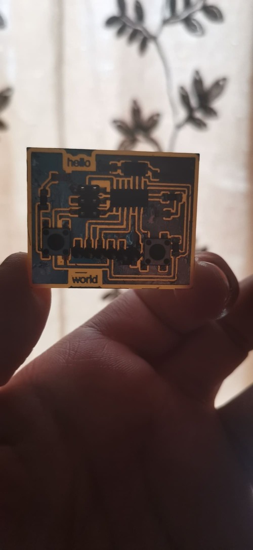
This is the final schematic look after completing adding the pieces to be added to the model
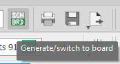
After completing my schematic stage to my next stage, which is that we place the pieces in a suitable place and connect them using the path tool
This will show the new window that we will be working on
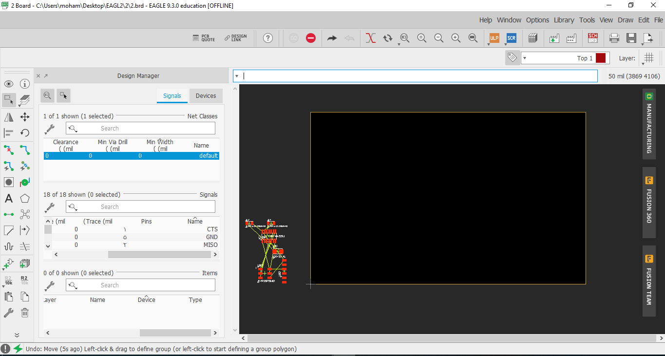
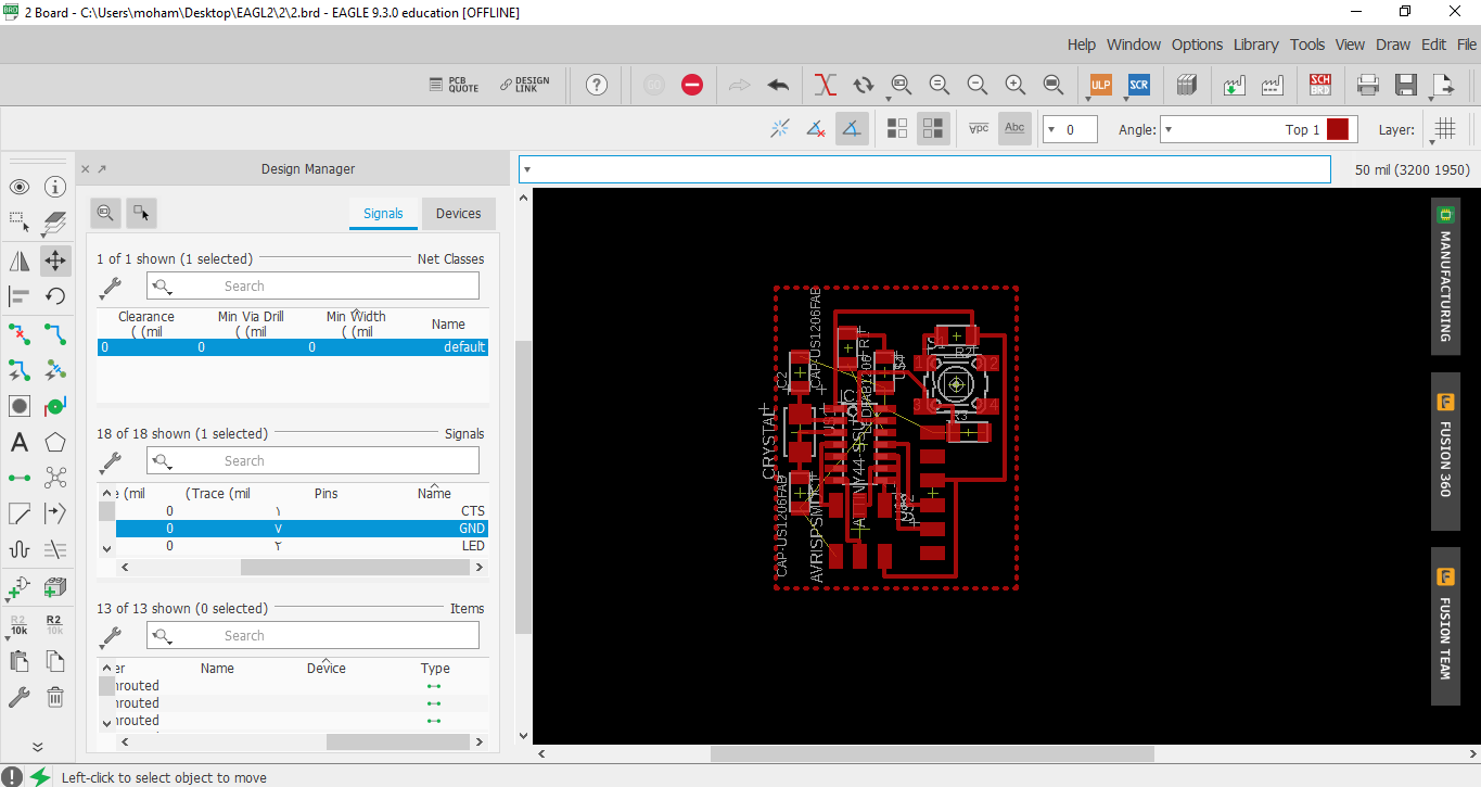
We select all shapes and move them to the middle of the black screen using (Ctrl + A), or we pull each part alone and then we connect the pieces so that each piece is in its proper place in order for the paths to be good and so that problems do not arise, the result will be as follows:
I drew a polygon around the design because I didn't connect the GND to some so I called the polygon GND in order for all the GND to communicate with each other.
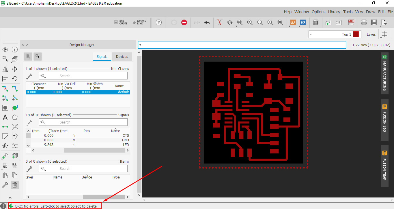
After all parts are connected to the appropriate location and the paths are drawn, we will verify the design using the Design Rule (DRC)
After completing the design, we will save the design in the form of one image for the tracks and another for the external cut
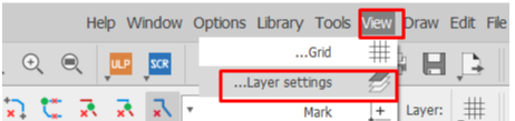
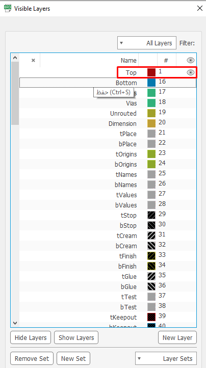
From the view tool from the menu, we will choose the layer settings command
After that we click on the command to hide all layers except the (top / pads)
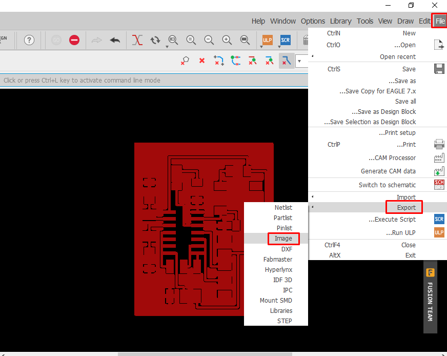
Then we export the layout in img format using the settings shown below
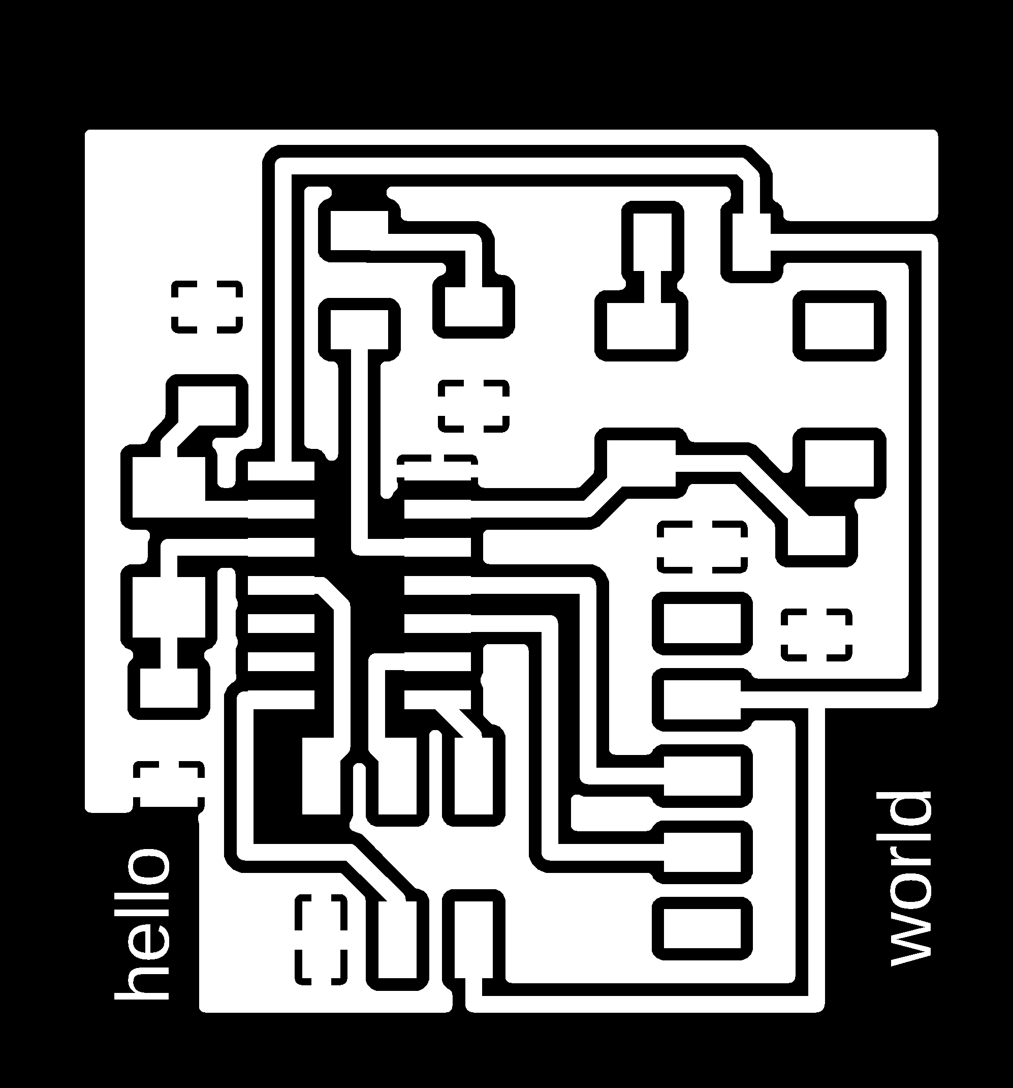
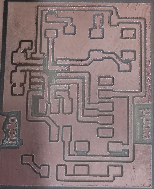
This is the picture for digging traces
For external shearing we hide all layers except for the dimensions, then we export the external cut in the same way as exporting the thr traces file. This is the external shear file

After that, we go to the fabmodules website in order to take the RML file in order to run on the machine like we did last week.Then we adjust the settings so we can dig and cut the board
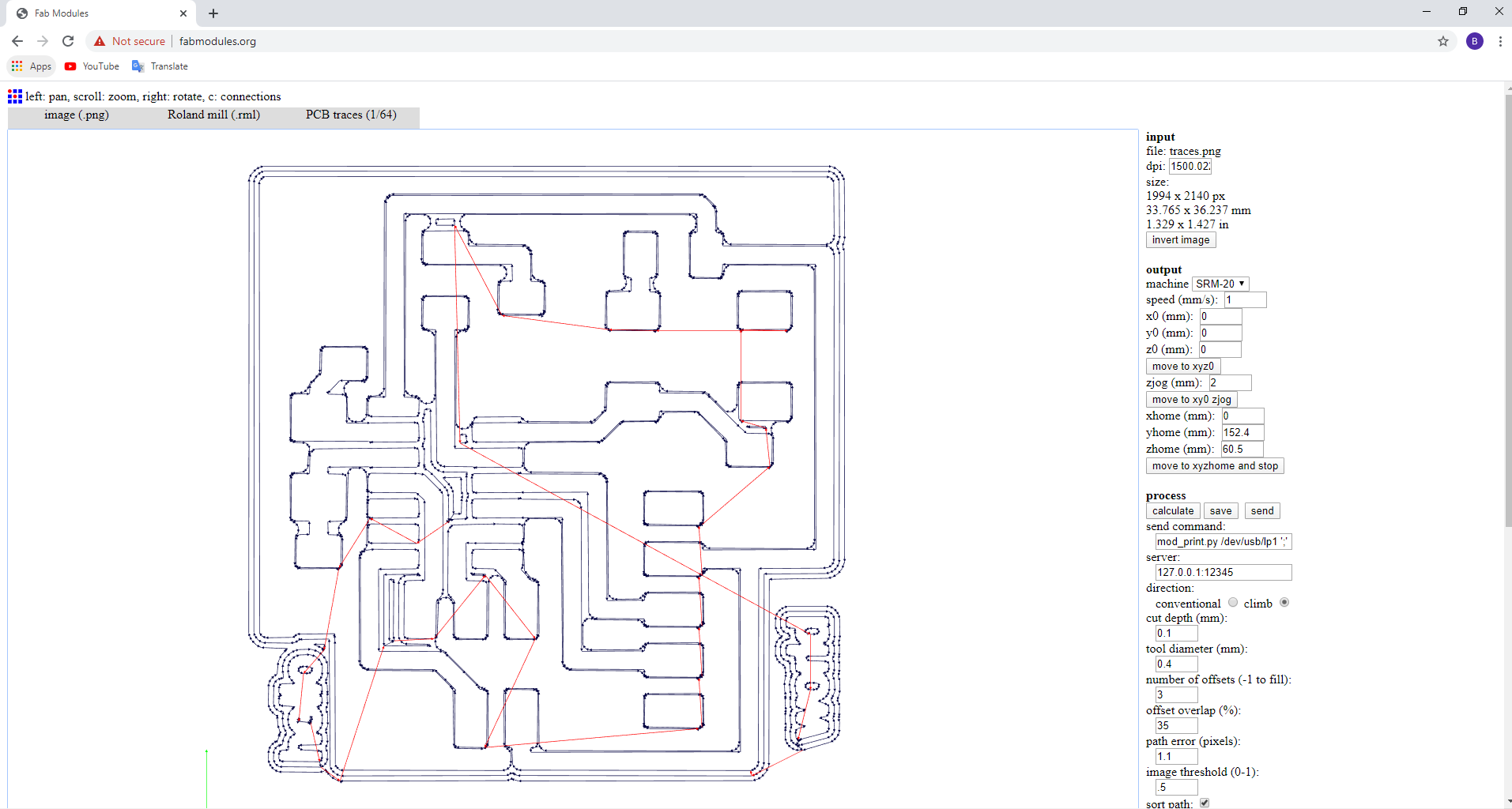
Also, we will use the external cut file, but with different settings.
Then we take the cut piece and then wash it under water and using a brush
Next we start soldering by filling a layer of tin on the surface of the tracks, and then wiping it with tape and flux.
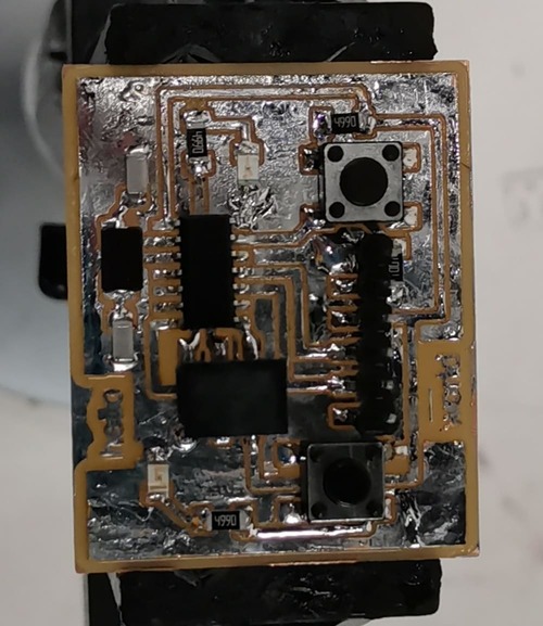
After that we start soldering and installing the pieces
We will need to set the Arduino program on ISP Arduino, on the Attiny family. After that we click from the Tools menu on the burn the bootloader.
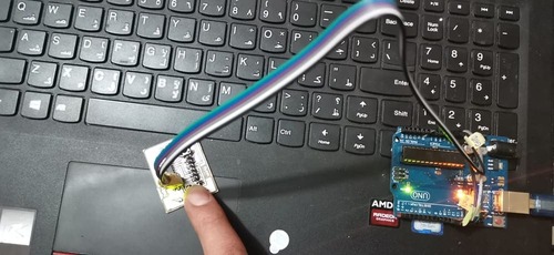
Just like we did in Electronics Production Week
This is the site for group assignments:Press here
group assignment:
use the test equipment in your lab to observe the operation of a microcontroller circuit board.
This link contains documentation for group work.