Week 7
Electronics Design
Objectives
Individual Assignment
Group Assignment
Learning Outcomes
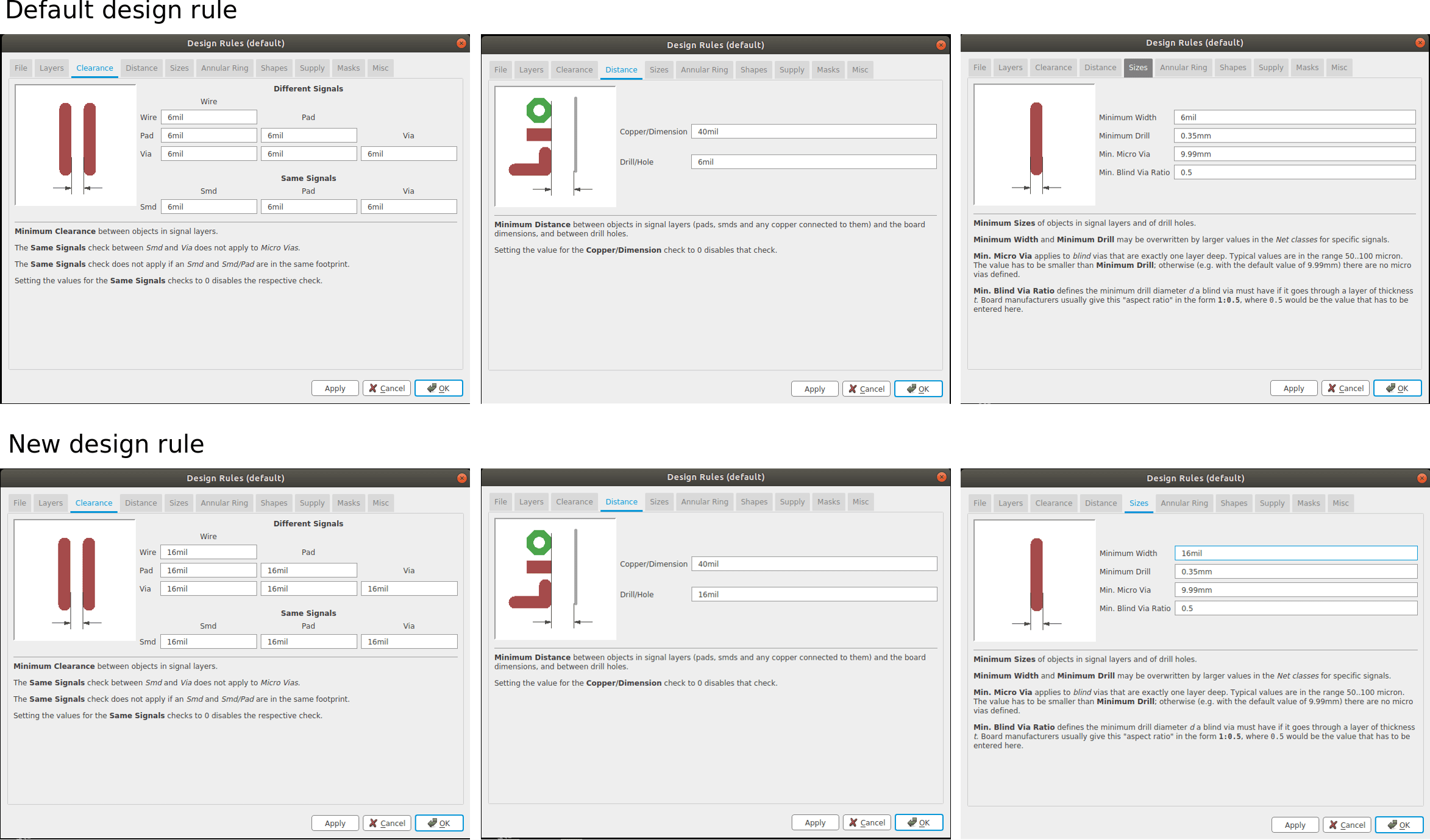
Individual Assignment
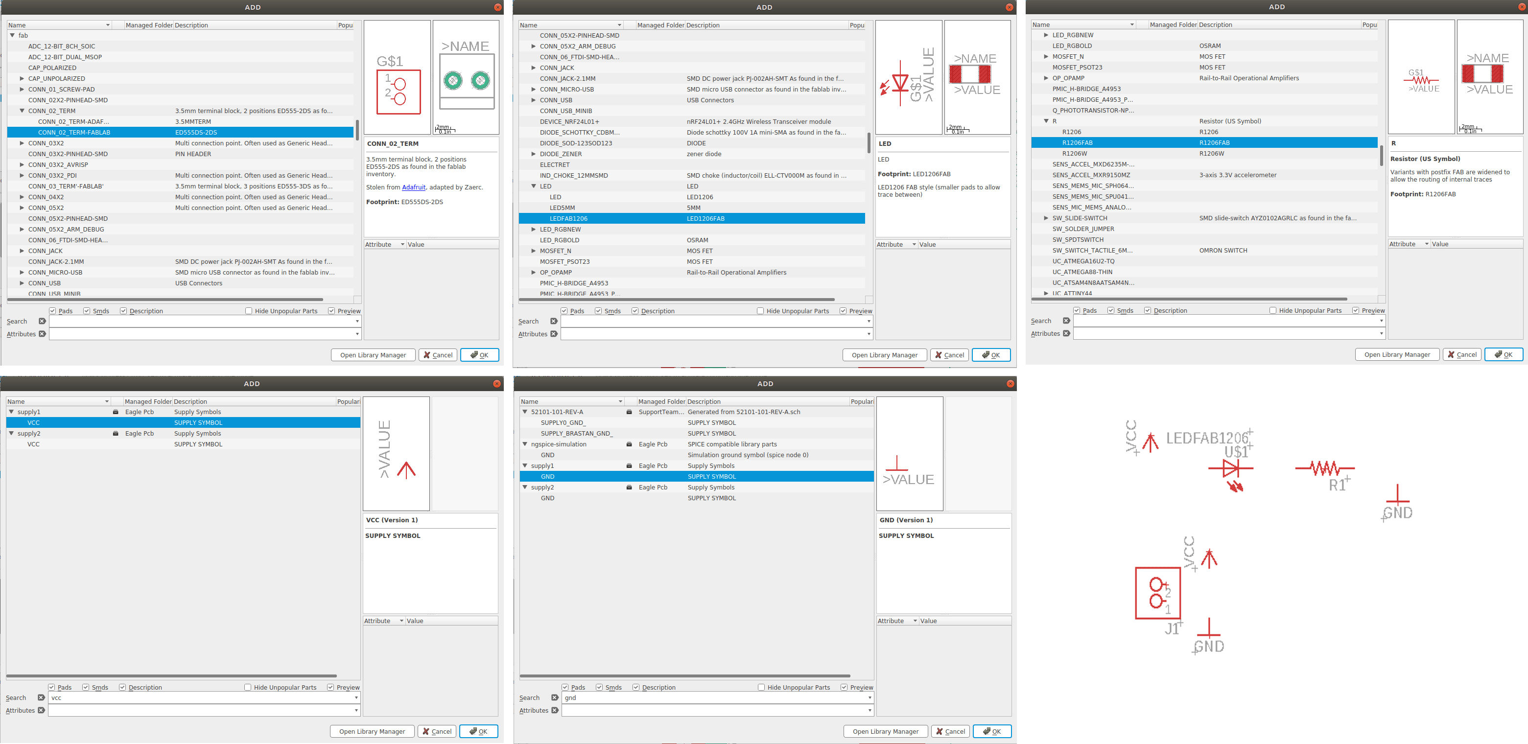
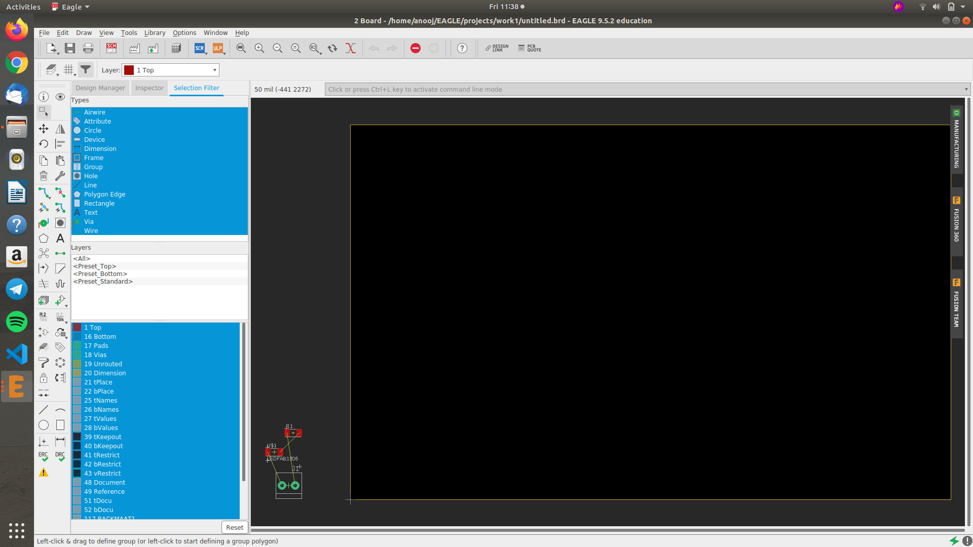
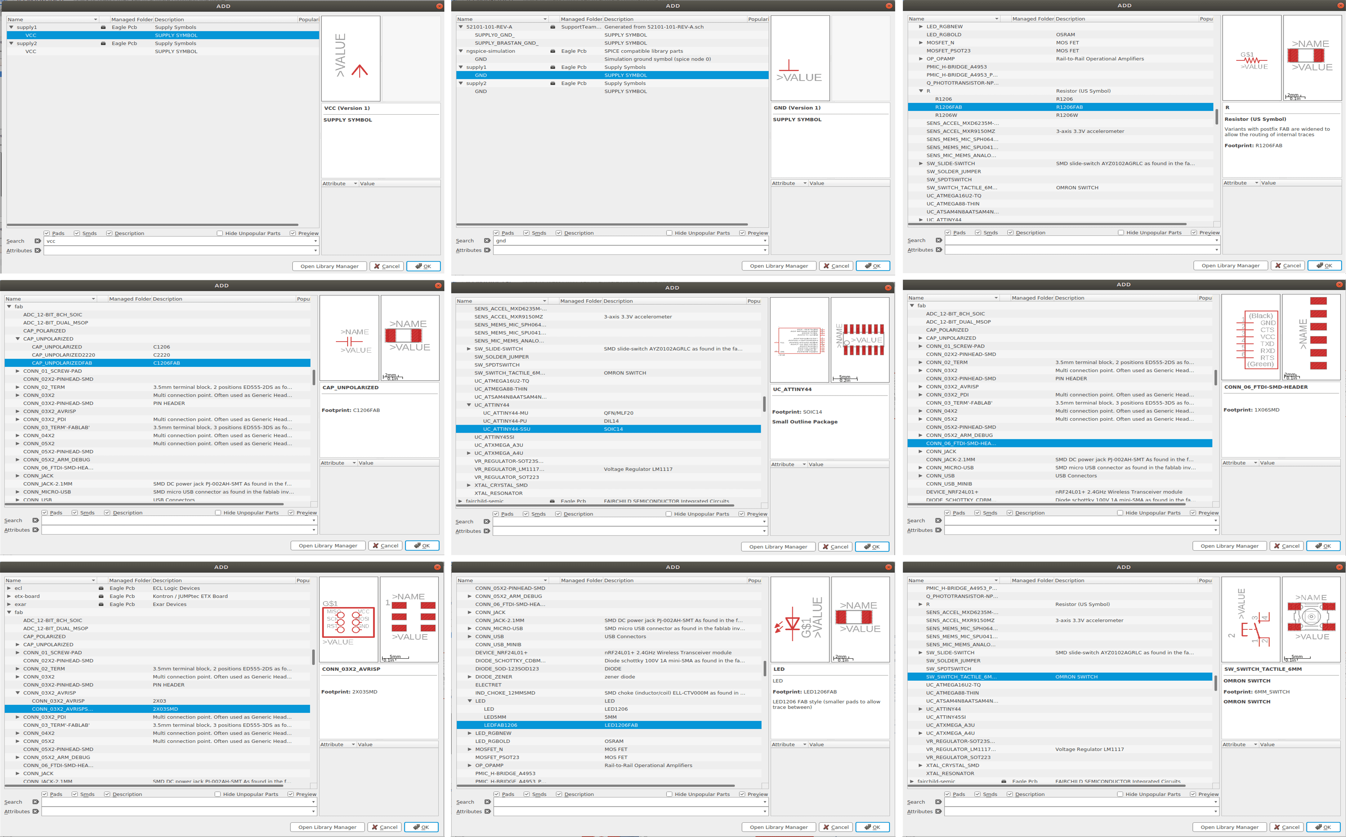
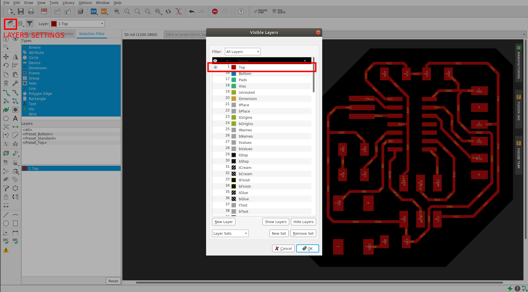
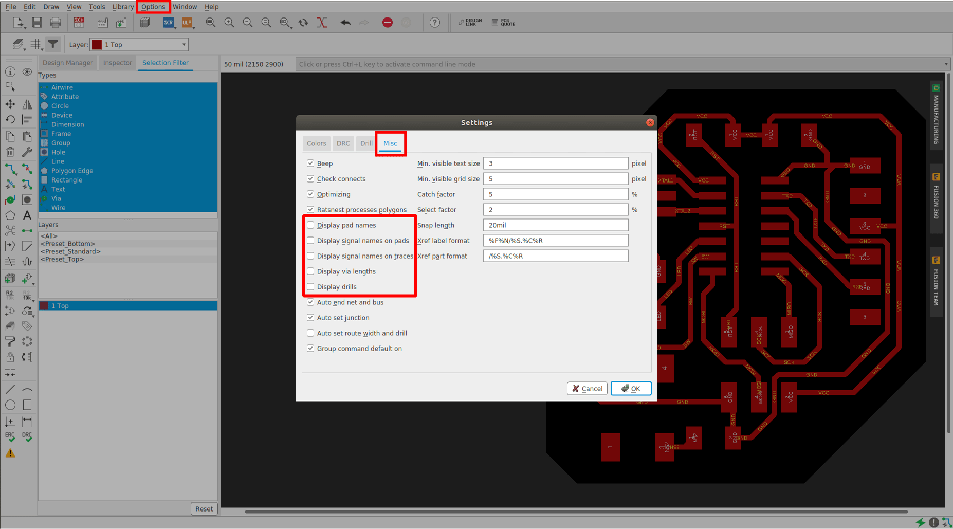
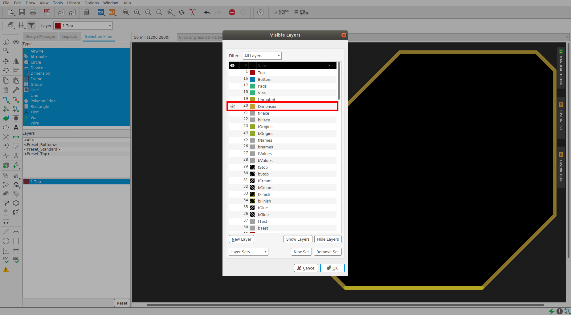
Autodesk Eagle

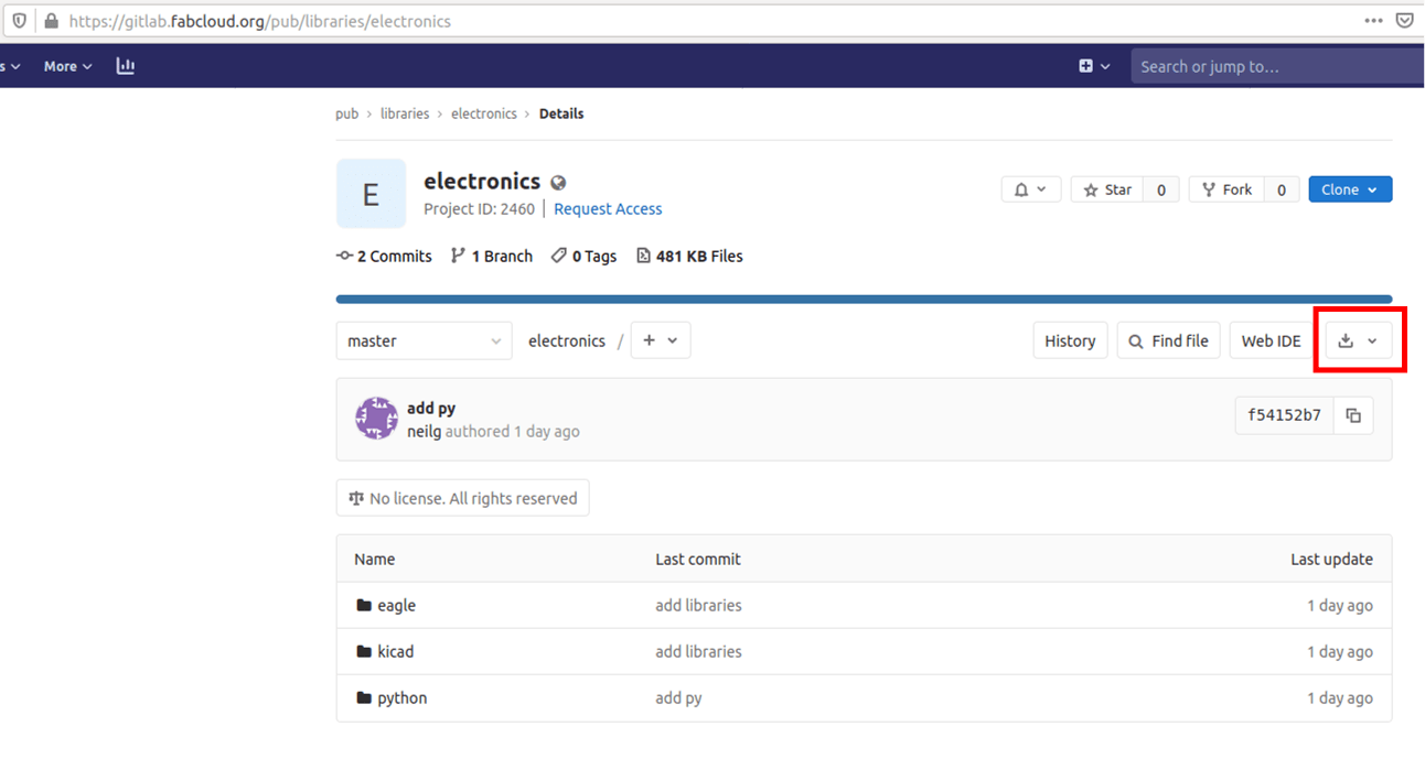
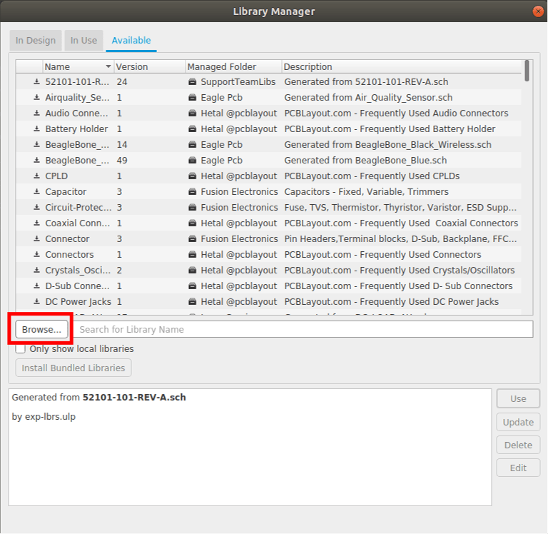
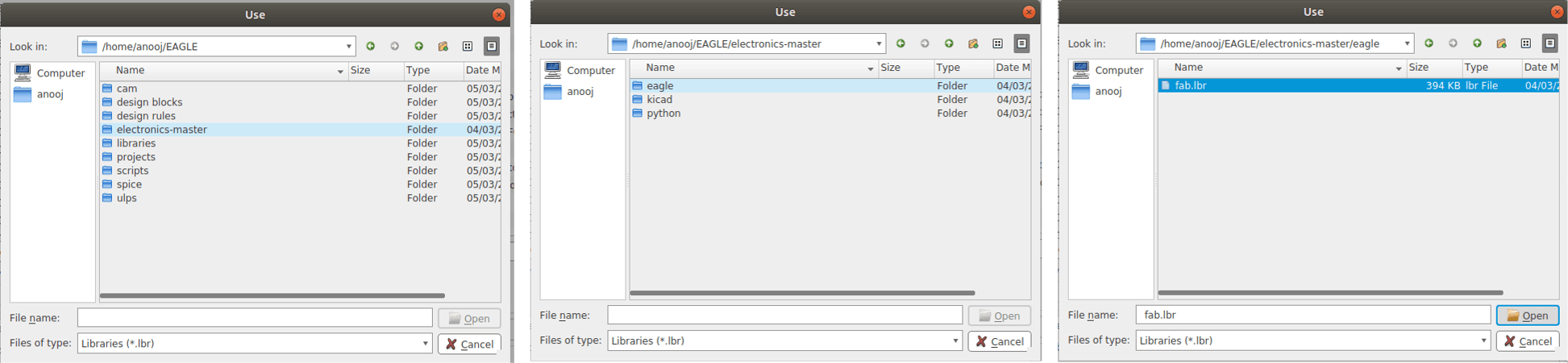
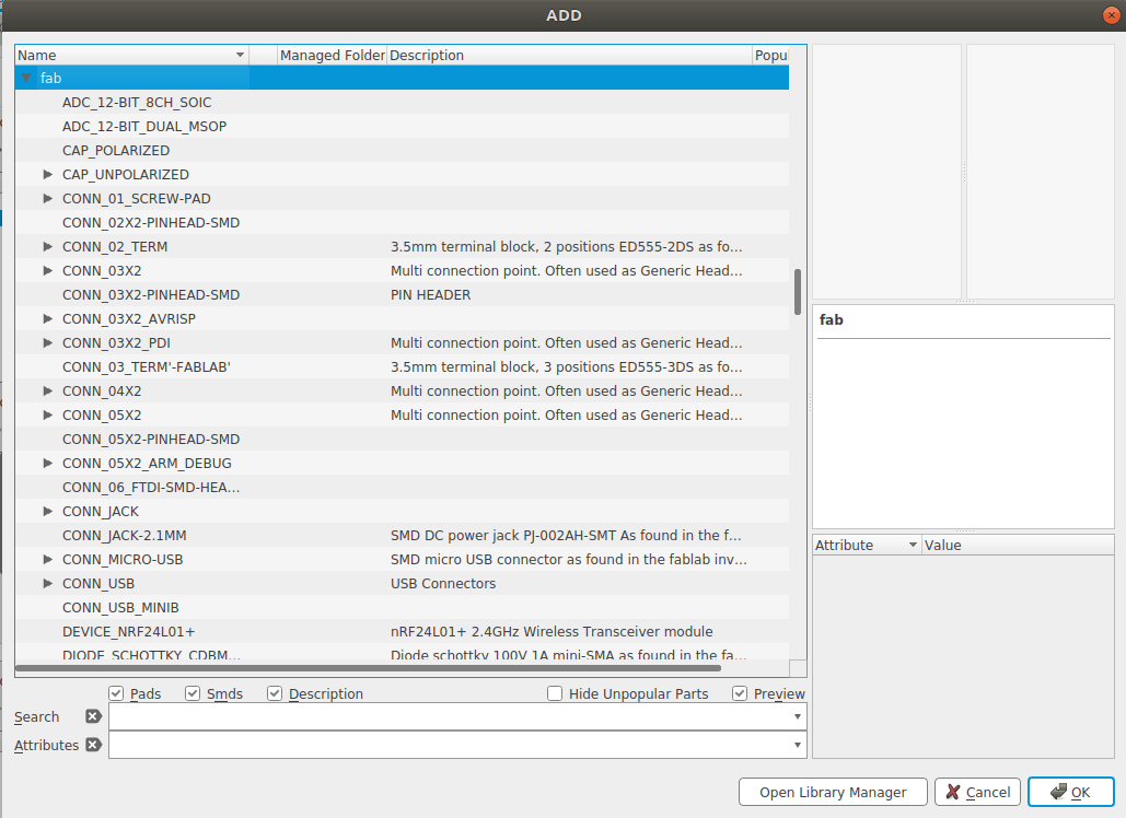
FAB Library
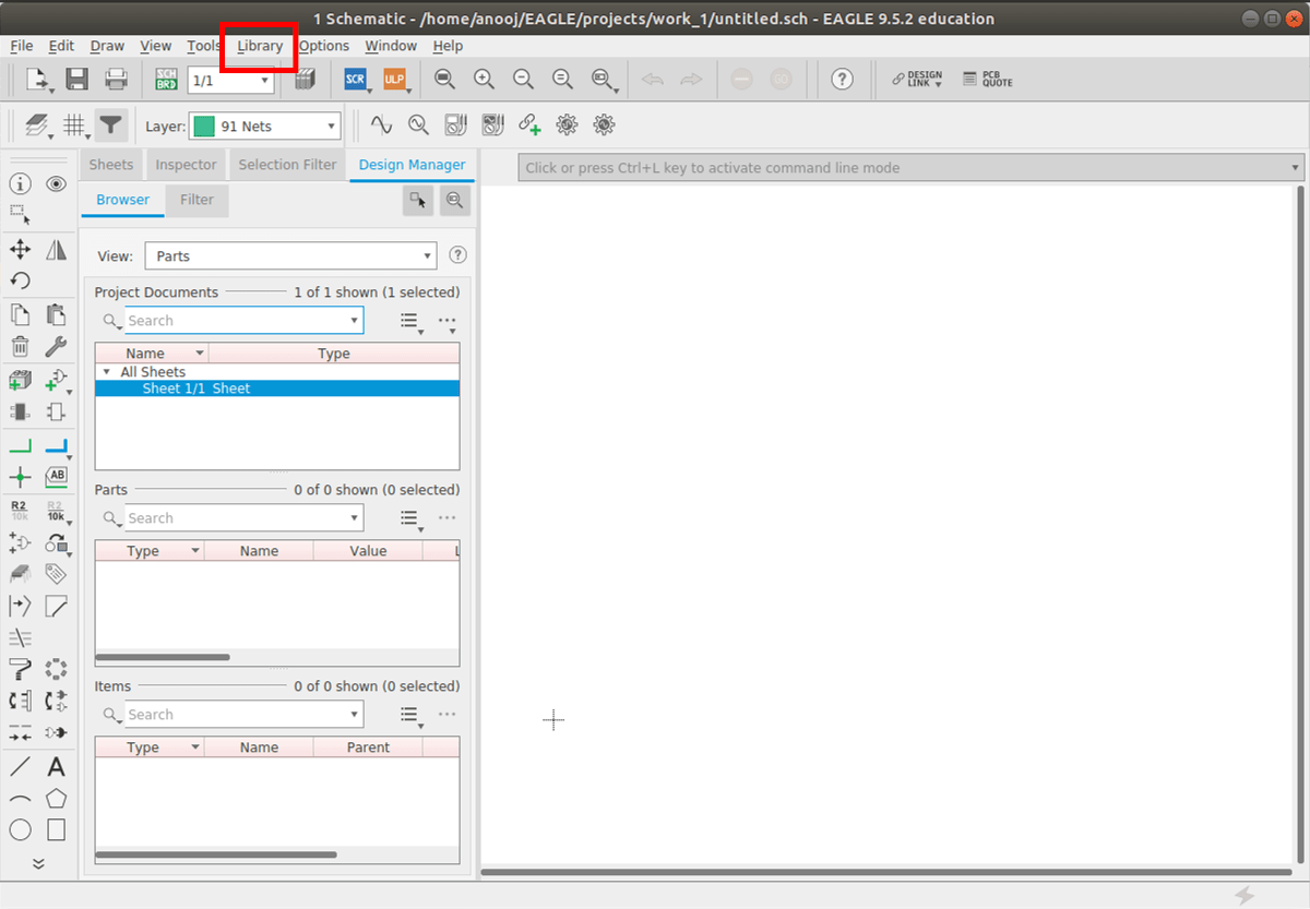
Learning Eagle
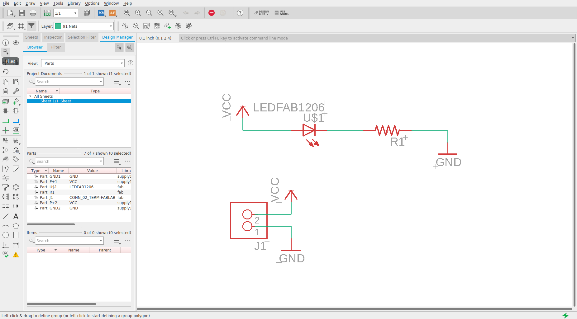
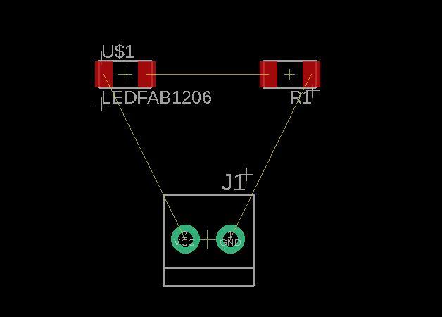
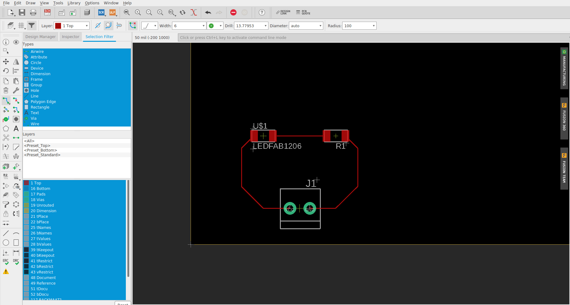
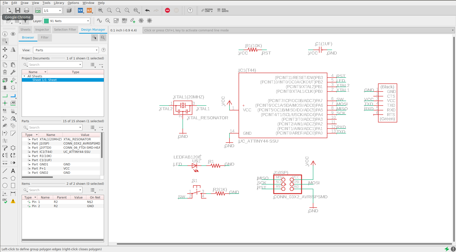
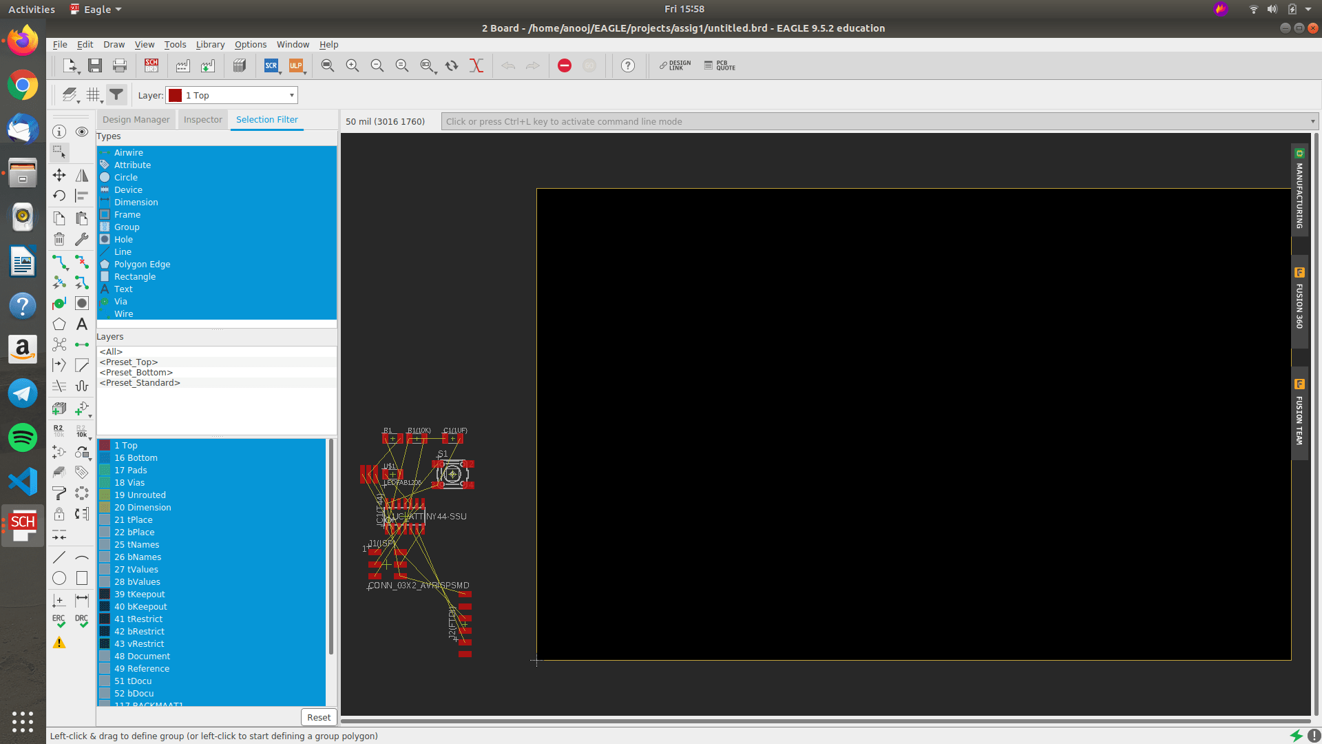
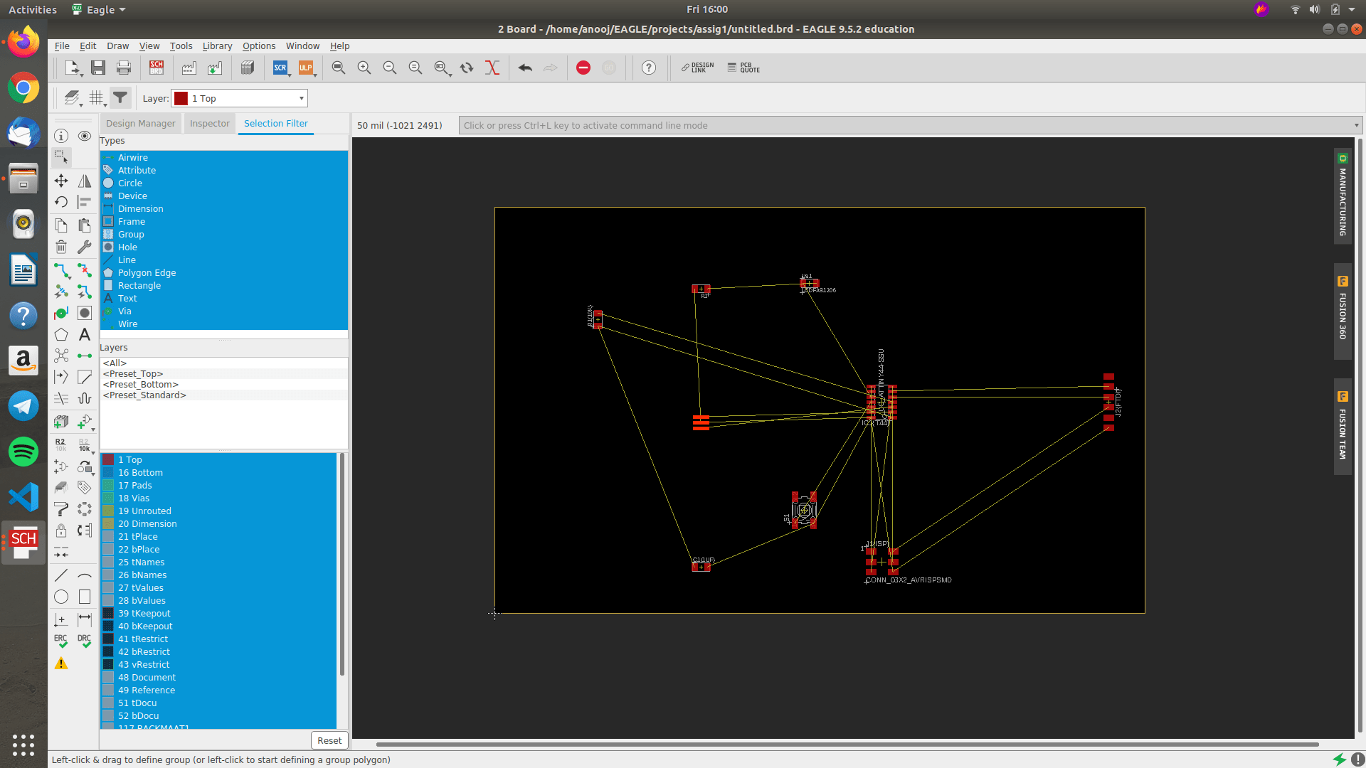
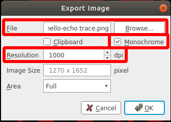
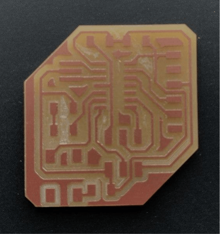
1) Redraw one of the echo hello-world boards, add (at least) a button and LED (with current-limiting resistor)
1) VCC
2) GND
3) Resistor
4) Capacitor
5) ATtint44
6) FTDI
7) ISP
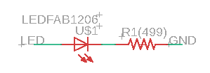
8) LED
9) Tactile switch
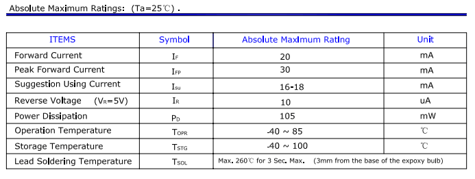
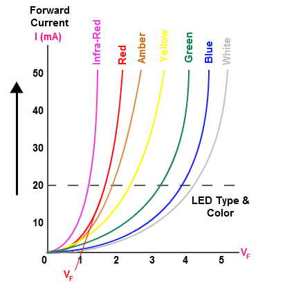
Vf = 2V
If = 20mA
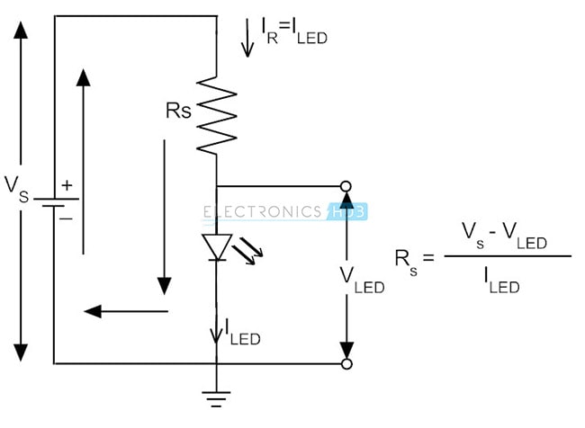
Rs = (5-2)/0.02 = 150 ohms
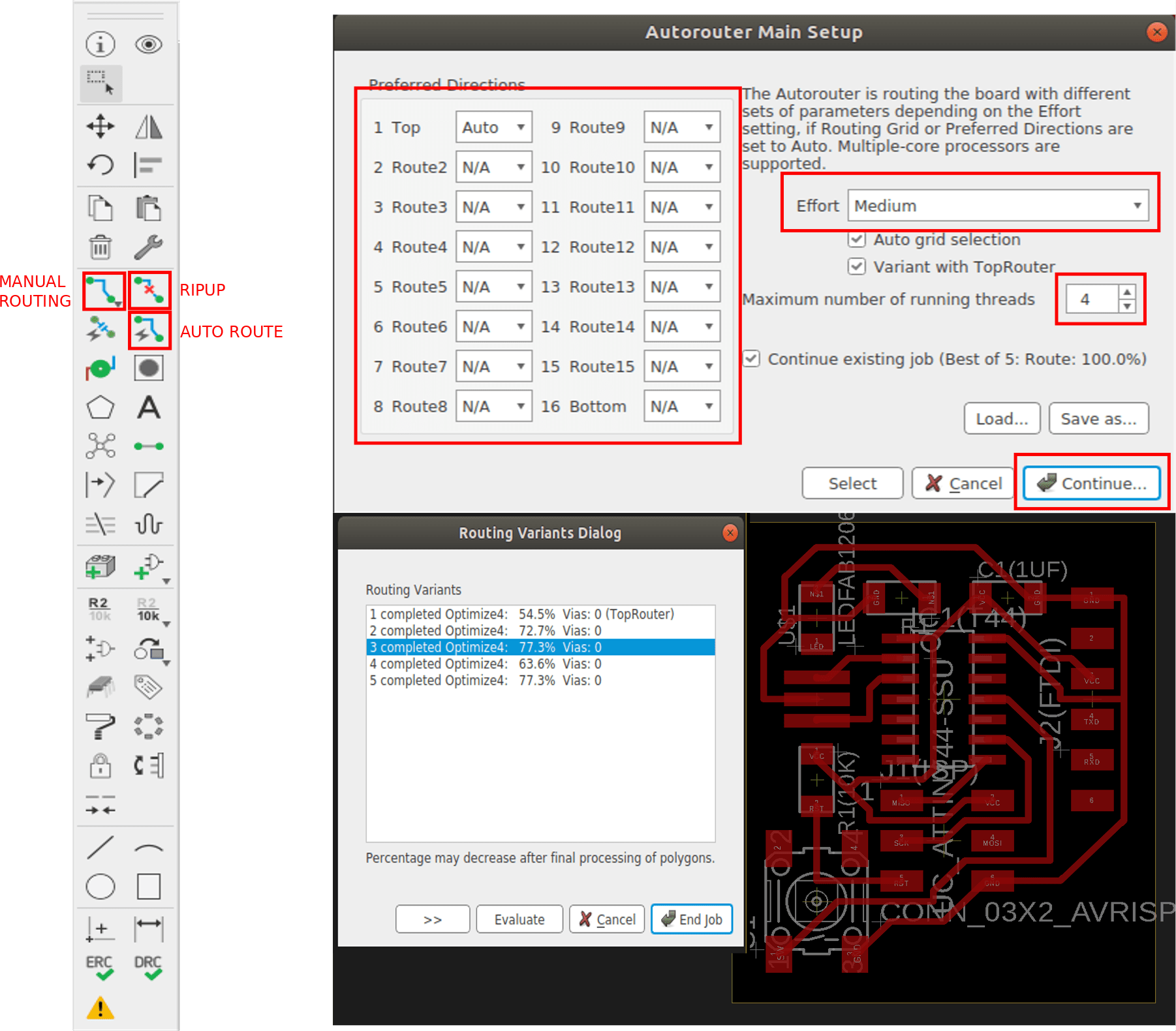
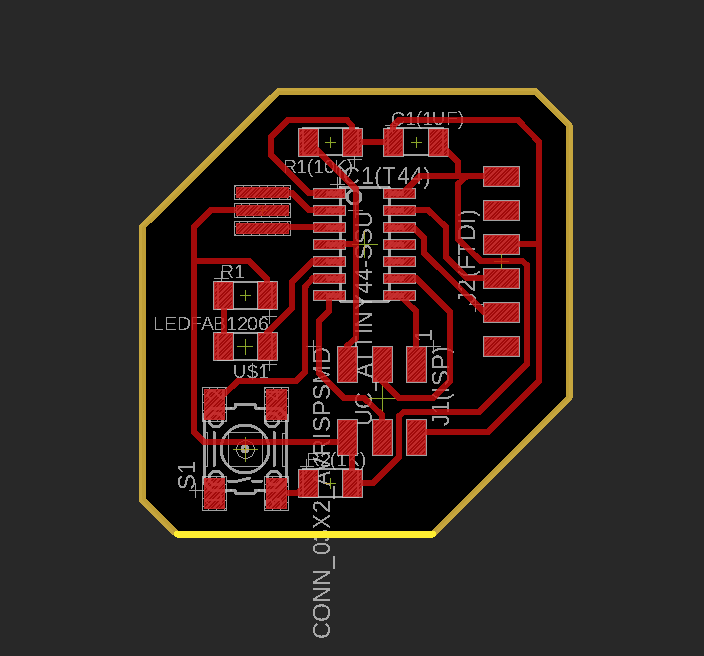
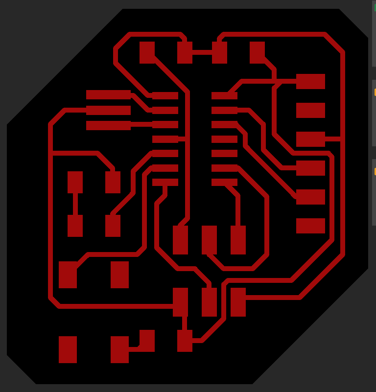
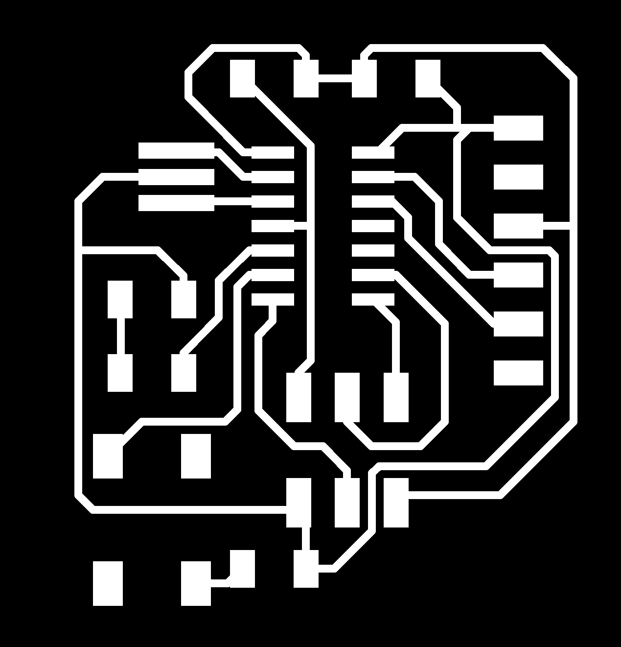

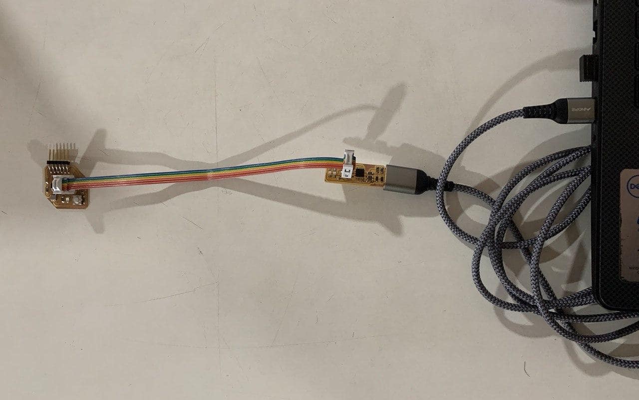
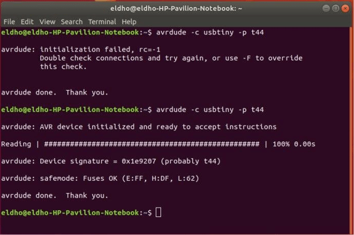
2) Make it
1)ATtiny44 - 1
2)ISP -1
3)FTDI - 1
4)XTAL 20MHz -1
5)Red LED - 1
6)Tactile switch - 1
7)10k resistor - 2
8)499 resistor - 1
9)1uF capacitor - 1
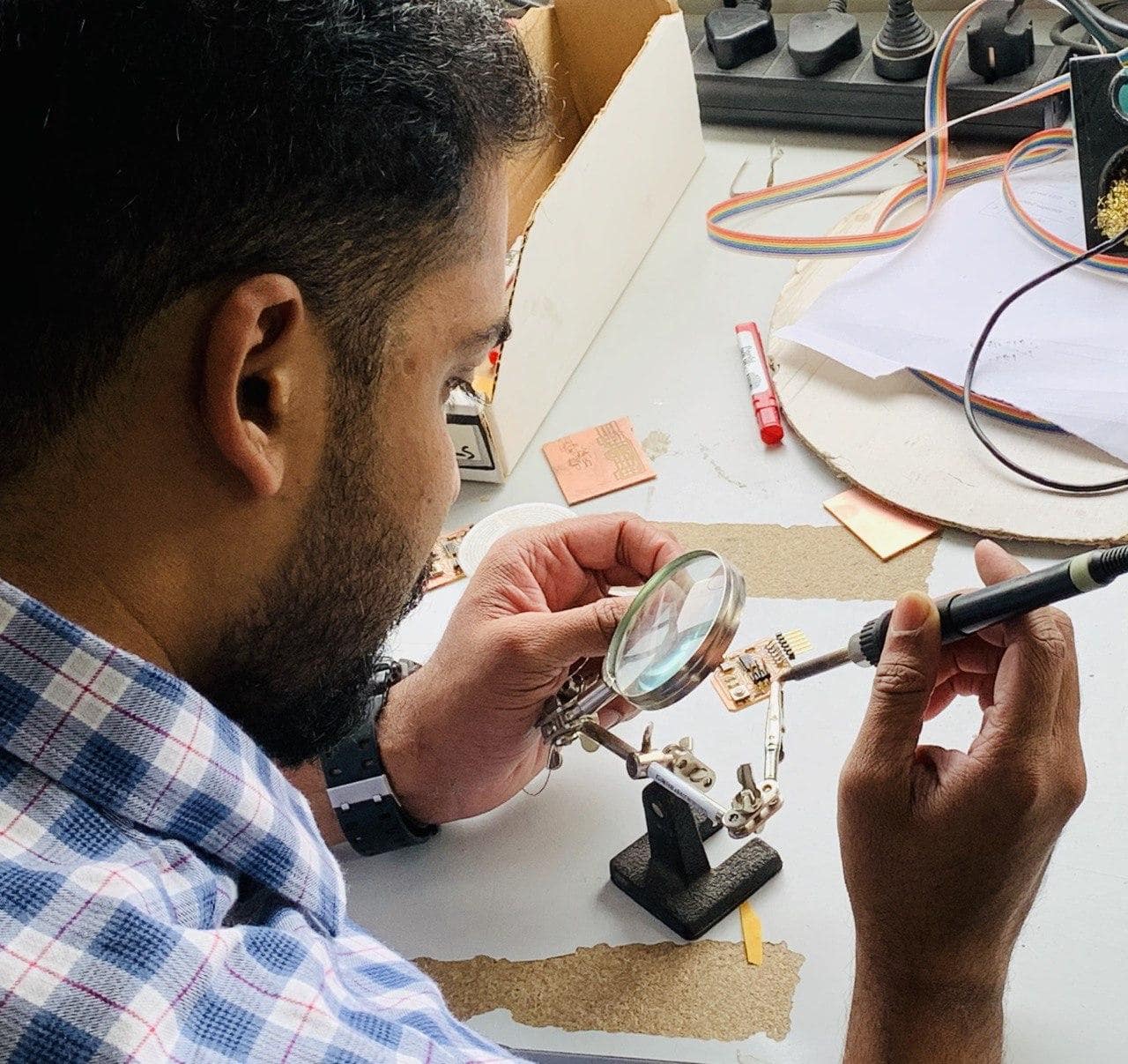
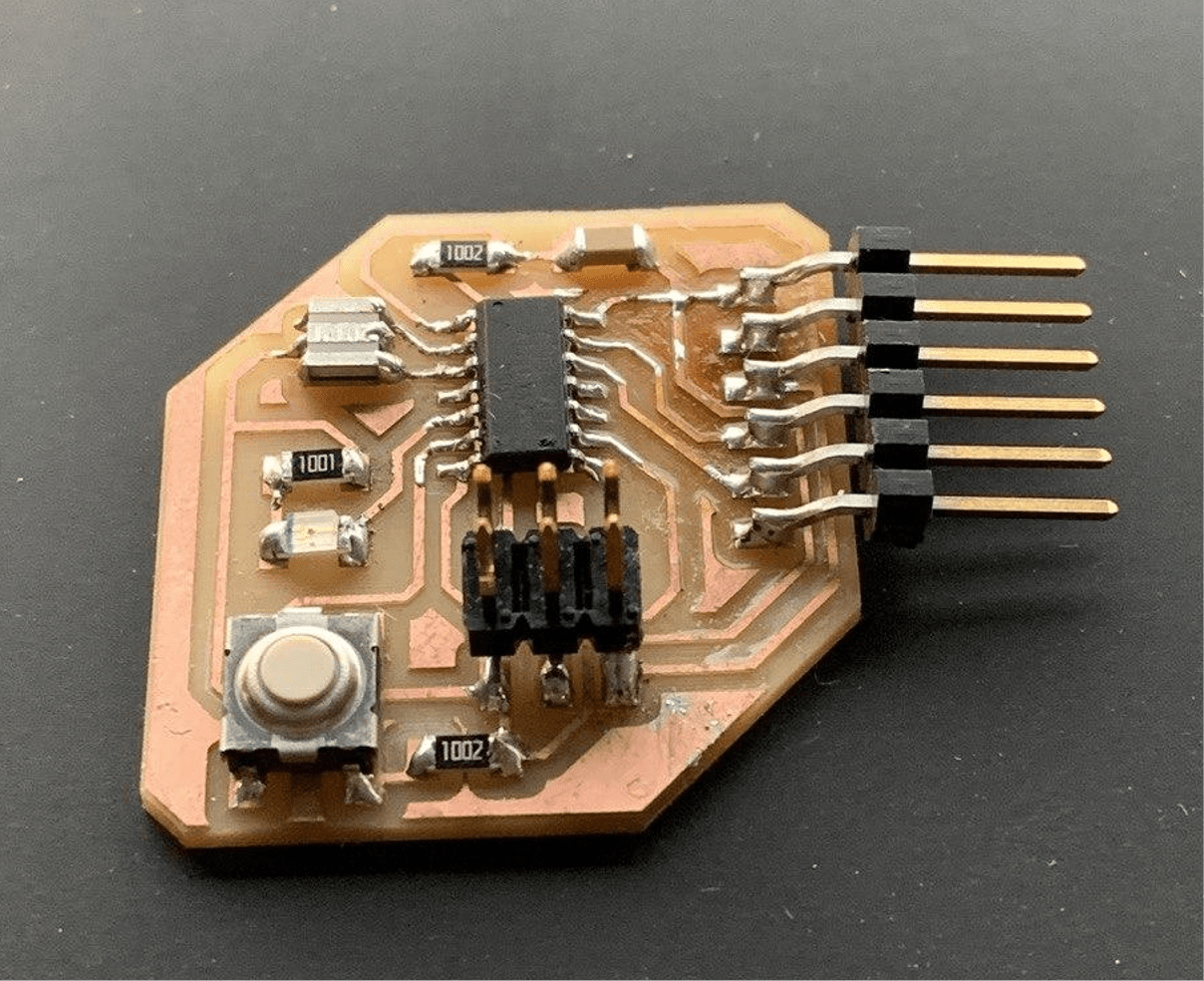
3) Test it
Make sure that the ground (GND) of both the boards are connected to each other.