Fabricate (PCB): FabISP.
Soldering FabISP components
Programming FabISP.
Design Circuit.
Schematic.
Layout.
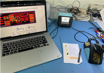
PCB Images / Design files –> fabmodules.
Milling.
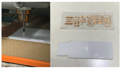
Fabricate PCB using a CNC machine (Milling).
Fabricate PCB using a vinyl cutter (flexible PCB).
Fabricate PCB using a fiber laser.
For this week’s task, we will Fabricate PCB FabISP. Afterward, I’m going to use it in my Fab academy Journey whenever I need to program any board or chip. Moreover, we took this chance to learn the steps of the electronic production of PCB.
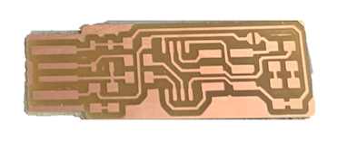
The first technique I did try this week was Milling which is a machine cut or shape materials using a rotating tool. I used ready made FabISP click for reference, PCB images were already (traces and outline), these images shows exactly carves that will be in the bored. What I need to do is open fab modules to convert PCB images into formate understandable by the machine that includes the movements of the machine need to do it to produce the bore
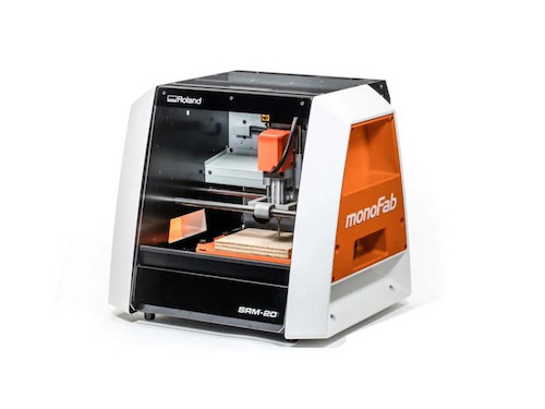
In the lab we are having Roland SRM-02CNC Machine its working based on milling technique , and CNC stand for Computer Numerical Control the picture below shows the machine:
Fab modules create .rml file because we did use a Roland machine that includes the movements of the machine need to do it to produce the bored.
The images below shows the input settings. I need to select for both traces and outline, they almost the same the only difference in step-1 for traces images I select PCB traces with (1/64 inch) size of the milling bit. On the other hand, for outline I select PCB outline (1/32 inch), the milling bit size effect how I want the bored to cut. For traces I need to graver, but for the outline in need to be snip the FR1 plate to separate the PCB.
For step-2 I selected the outputs, first the machine available in LAB is SRM-20, step-3 selecting the reference points for X , Y ,and, Z .
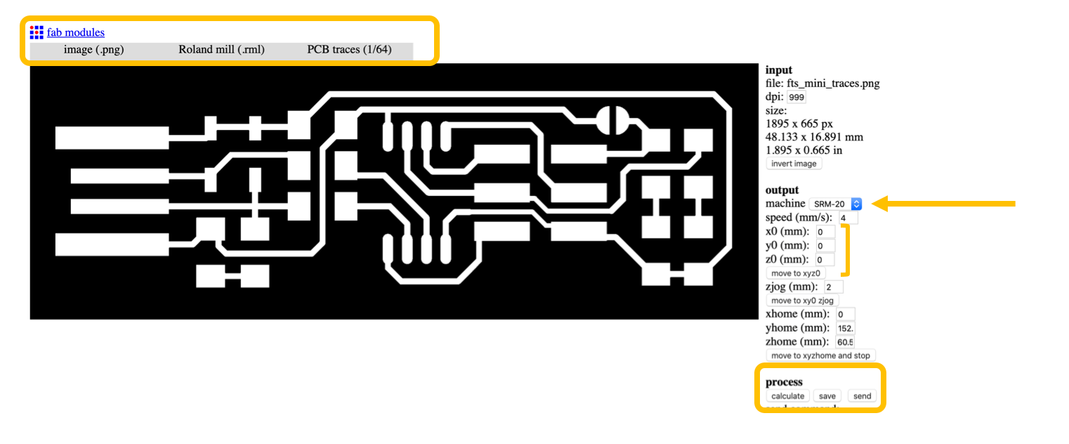
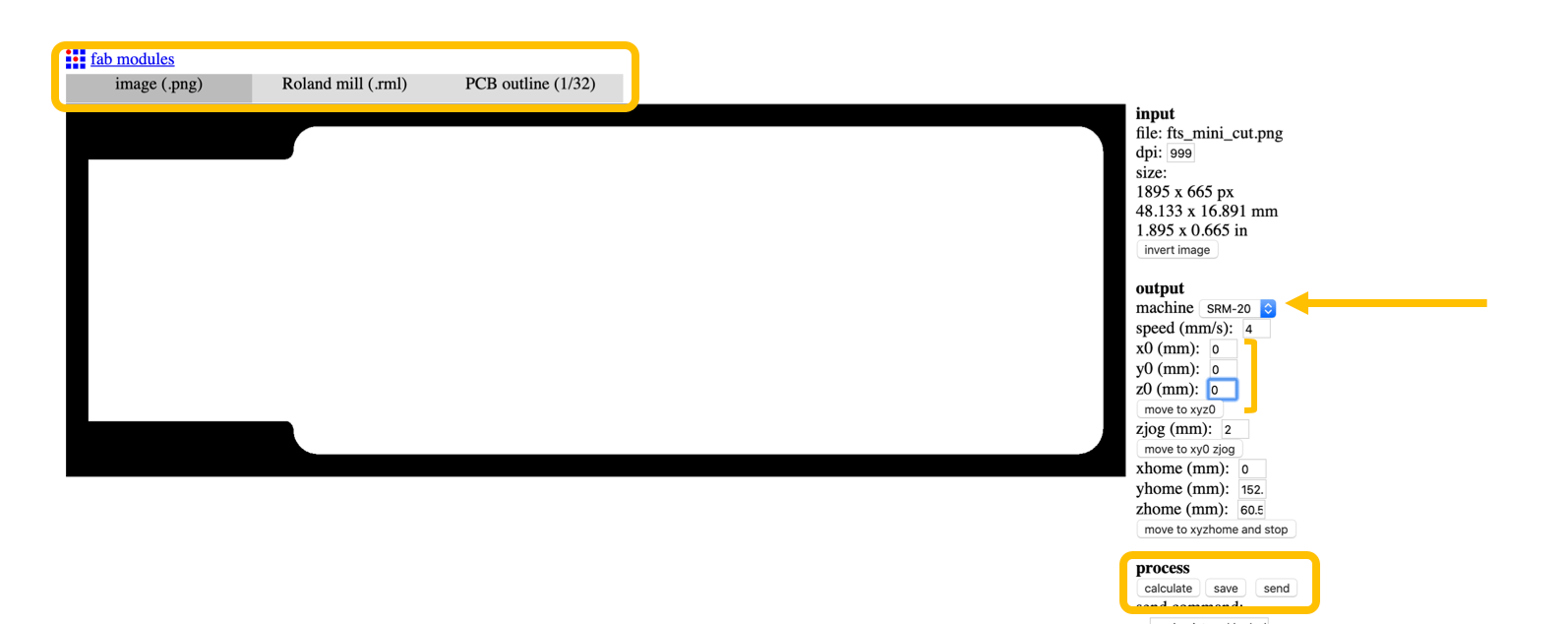
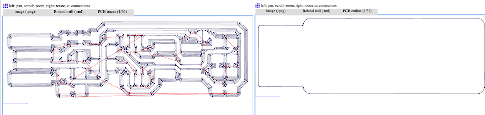
Finally, the last step-4 press calculate this will generate Roland mill file, then save it to use after in the software, the figures below shows the paths the milling bit will make.
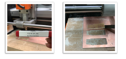
for the material I did use what available in the lab which is FR1 and its safe compering to other materials in market.
As we will use the same FR1 sheet to save materials & avoiding any waste, so we did The set up together.
The above pictures show the steps of milling the traces. First, I did use milling bit size 1/64 inch ,and, I use V-panel for SRM-20 to set the origin point for X Y Z ,whenever I’m done I press cut and add trace file.
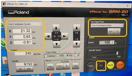
For the outline is the same steps but I changes the milling bit to 1/32 inch, and I only set Z origin without changing X and Y , Finally I took out the PCB out as shown above figures.
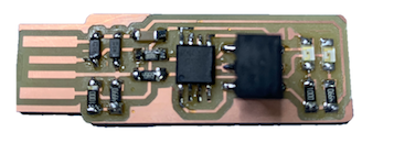
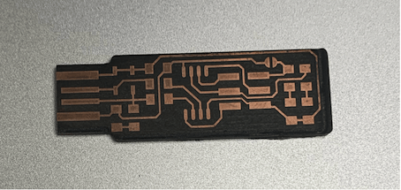
Finally My PCB is Ready, Now I can start Soldering
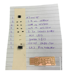
I did start by organize the tools in my solder station as shown in picture below, I always enjoy soldering especially SMD components, because it lets me feel relaxing and I love to see the board full of components in the END.
Heat and clean the iron to look shiny.
Heat the pad.
Place some of the solder in one of the pads to fix the component from moving, as it easily can be moved. with one hand I hold the iron, and the other one I hold the component with tweezers and align it in the pad, then heat the pad has the solder.
Add solder to the other pad.
Re-adding the solder in the pad I use it for fixing the component.
After I finished soldering it’s important to remove the extral solder between the pads to avoid short circuits.
My PCB after soldering:
I will need to use this connector in case I want to program any PCB through my FabISP.
Equipment :
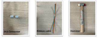
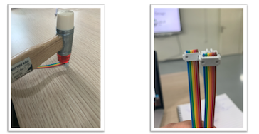
I did insert the 2x3 connector from both sides of ribbon cable, then I used the hammer to lock them as shown below in picture.
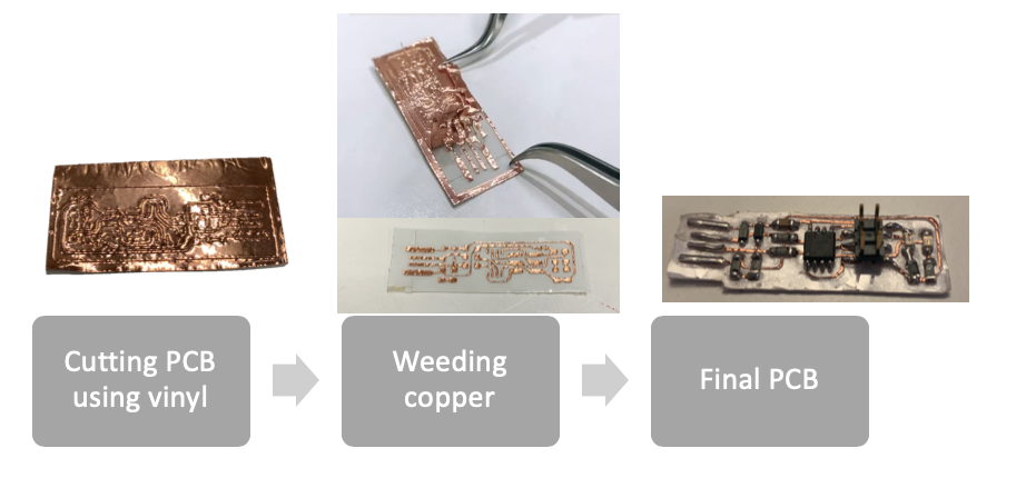
The second technique was fabricating flexible PCB using a vinyl cutter, to come out with the best settings to cut the PCB we worked as a group for details please visit our assignment group page.
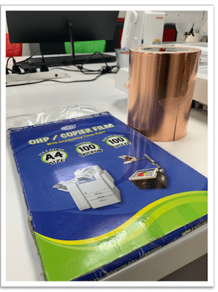
Copper foil tape.
Transparencies (OHP / copier film with interleaving Tissue paper)
Tweezer.
Plastic card.
Placed the copper foil at the transparencies, to ensure the copper will cut well.
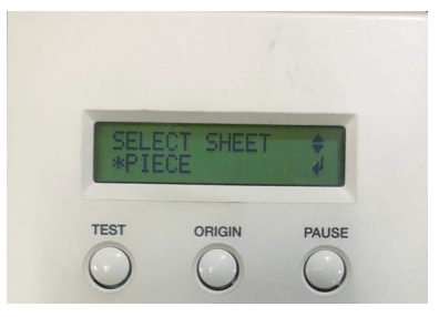
Load the sheet into the vinyl machines.
Choose in the machine select sheet type: piece, and note the dimensions of the sheet appears in the machine for afterward using at the RolandCut studio.
Open the trace image in RolandCut studio the image must be in .JPGformat, after open the image the dimensions, may scale, so I need to fix the dimension by checking the dimension in fabmodules and change it, Finally, we must change the image form raster to vector.
The perfect pin force for cutting the copper, which was obtained from the group assignment after a lot of trials is 140 gf.
As shown in the images below the PCB after cutting.
Afterward, removing the excess parts of the copper (weeding copper).
Before soldering we paced the FabISP in cut outline plastic, to ensure the stability of the PCB. Moreover, to cut the card we used CNC machine.
Next, I did solder the components and programmed it as before, and, the flexible FabISP was working perfectly:
I faced some problems while soldering because the pads and traces were not fixed at its place and easily can be moved, I had to be careful and focus while soldering.
In addition, the traces easily can be removed, When I was removing the connector cable while programming the fabISP I cut one track by mistake, but I fixed the connection by adding solder as shown below:
It was a nice experience to make flexible PCB, I always wanted to make one, also I really love how the traces look in the transport paper.
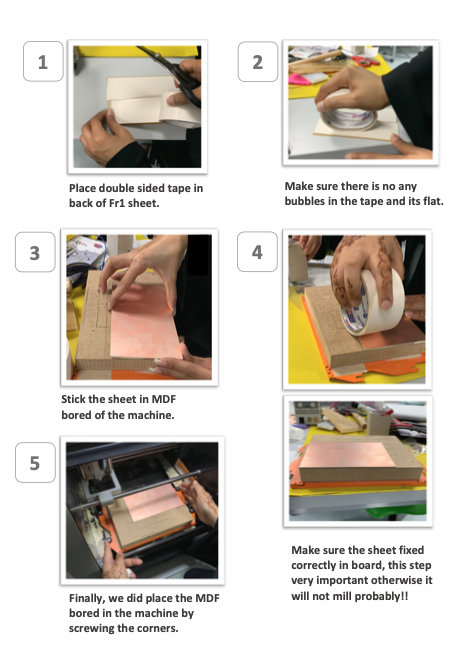
The third technique I did tried was fabricate PCB using fiber laser, we worked as group to characterize the design rules of the PCB produced with Trotec laser, for more details visit the group assignment page.
Needed Equipment:
MDF board.
FR1 Copper Sheet.
Double face tape.
In short, we started by stick the copper sheet in the MDF board, then I opened CoralDraw and prepare the fabISP PCB image to engrave, Next, I opened the laser software and insert the perfect setting obtained in the group assignment.
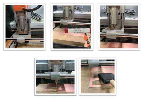
After finish engraving, I added the outline image, and, repeated the steps we did for engraving
Cutting the PCB was not that easy as we were printing all the PCBs together. We must be too much careful while cutting, and keep the lens position in the same engraving setting place, if only one centimeter the lens moved the cutting will not go well, this movement may cut the traces in the other PCBs. We did a lot of cutting attempts until reaching the perfect one, for more details my friend Maha page.
In the end, we decide to cut them using the milling machine, because unfortunately, we changed the position of the lens, and we did try to place the lens to the nearest place as before. However, it was not an easy job, so milling was the easiest solution.
As shown in the image below the PCB produced using the fiber laser:
I didn’t get the chance yet to solder it, when the lab is opened I will solder and program it.
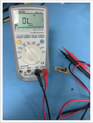
To insure there is no short circuit before plugging the FabISP in laptop otherwise it will burn, I did continuity test using multimeter as shown below in figure.
Note : Many thanks to my colleague Shaikha also a mac user finds out the commands we need to type, as we did face some problems while installing because of the new update of Mac
version 10.15.2macOS Catalina not compatible with corssPack version.)
Install Homebrew
Type:
brew tap osx-cross/avr
ruby -e "$(curl -fsSL https://raw.githubusercontent.com/ Homebrew/install/master/install)
brew install binutils
brew install gcc
brew tap osx-cross/avr && brew install avr-gcc
ruby -e "$(curl -fsSL https://raw.githubusercontent.com/Homebrew/install/master/install)
Brew install avrdude
Restart terminal then type:
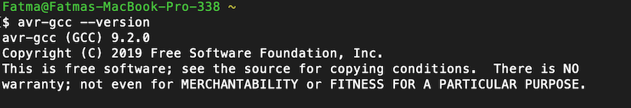
avr-gcc --versionTo ensure the right version install in the laptop type :
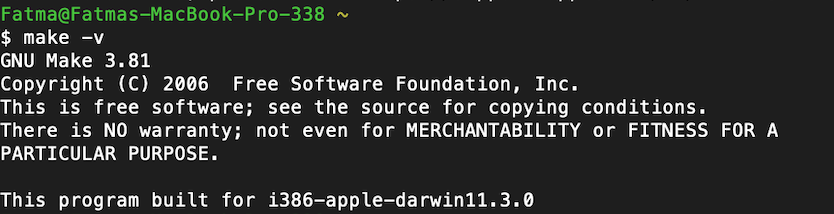
Make -vThis command insure that
makecommand is working
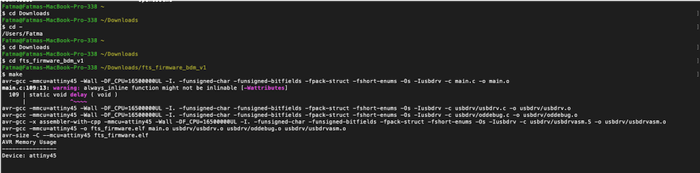
Extract the zip file –> open terminal cd to directory I want save in file –> Run make.
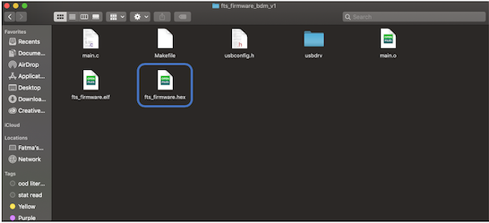
when running is done, a file called fts_firmware.hex.created see the picture below:
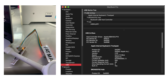
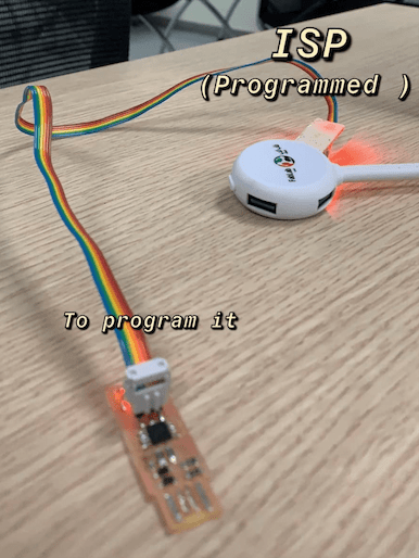
make flashNow after finishing install all needed softwares it is the time to program my FabISP there is 3 commands to type on terminal, first I need to cd in directory I have the fta_firmware.hexfile and do the connection shown in picture below, Moreover I did use a Hub because the USB bus in my device is USB 3 and FabISP working only with USB 2 :
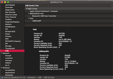
make fusesNow, I need insure that my Mac recognize my FabISP from system report as shown in image below
make rstdisblIt will blow the rest fuse. After Doing this step I will not be able to program my FabISP with another ISP programmer once the rest fuse is burned.
Now I have ready programmer FabISP.
A image of working FabISP
Before all else, I need to prepare board for the for first time use.
First I did update Arduino IDE to the last available version which is 1.8.10.
Connect my board with FabISP through the ISP header using a ribbon connecter, and I need to make sure the laptop recognizes USBtinyISP.
Open Arduino IDE, download ATtiny 44 board, then selected Tools > Borad > Atting44 as shown in the image below
Next, select the used processor, port, and, clock.
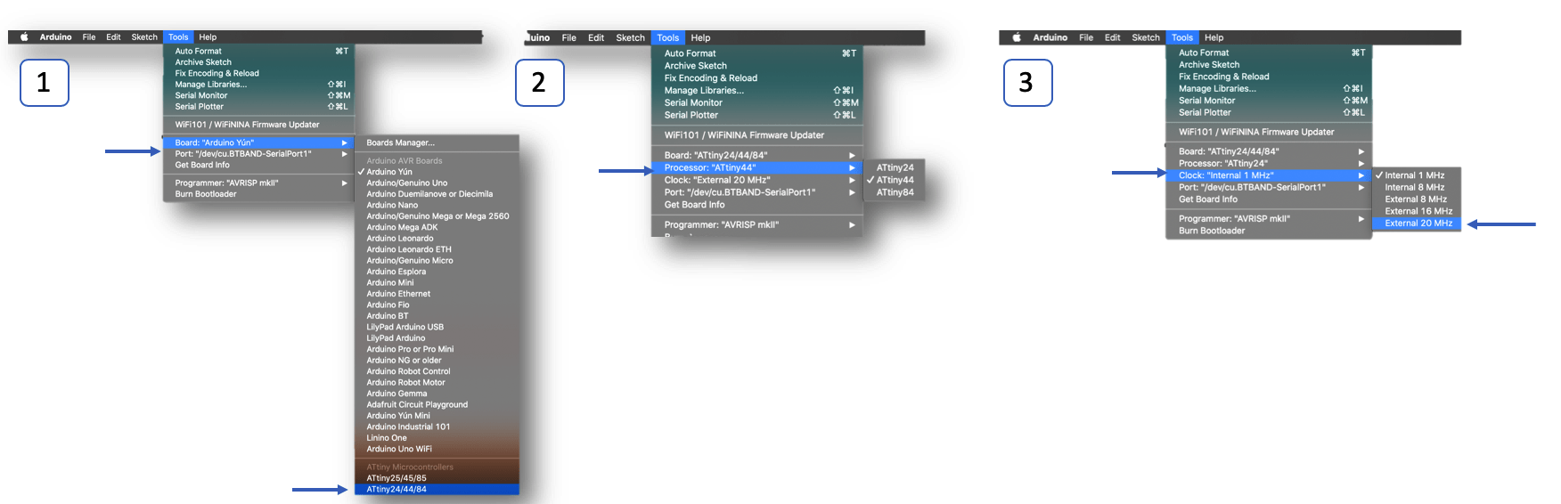
Select the programmer, then go to Sketch > Upload using programmer
Go to Tools > Burn Bootloader.
Here the below video showing the fabISP working perfectly. as it was used to power and program the ATtiny44 board.
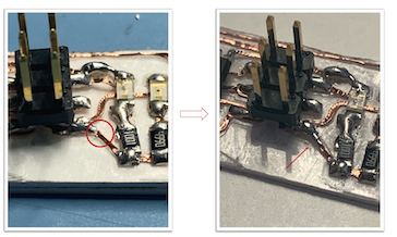
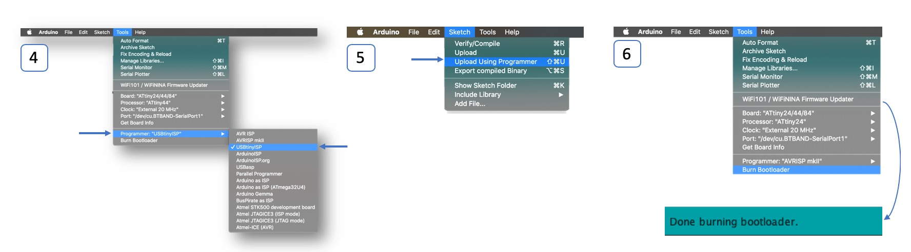
I faced a lot of problems while programming the board, First I plugged the connecter cable in the wrong direction with ISP headers, so smoke starts coming out from the ATniy45 chip, therefore, I burned it I went to de-solder the chip, but I did use Wick and this was my biggest mistake because it took from me a lot of time, and, I end up cutting some of the tracks and pads in my PCB.
For the second time, I did also burn it because I reversed the connection between the ready programmer fabISP and my fabISP when I do plug it to the laptop.
For this time to De-soldering, I did use a heat gun, but Unfortunately, I aimed to desolder only the damaged ATniy45 but I did de-solder the near components.
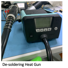
I think I did this mistake because I did the set the heat very high and I didn’t direct the gun in the correct place.
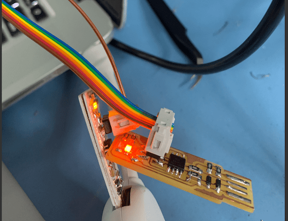
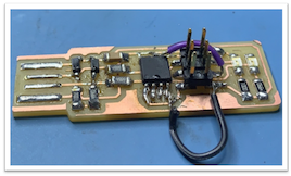
However, I didn’t lose the hope of using the same PCB, I used wires left from used ribbon cable available in the lab to do the needed modification on connections see the picture below showing my first PCB with all adjustments I did to let it work.
Still, whenever check the connections there was a short circuit in the PCB, also I can’t find the error with all debugging I did, everything seemed good, but the multimeter was indicating for short circuit.
Unfortunately, I can’t use it anymore :( it took for me so many hours trying to fix it, I was hoping using it even it was looking ugly because I was making effort to make it work.
Troubleshooting is a very important step before plugging in circuits board to the power supply in my case the laptop, after I go through all these problems there were 3 steps I make sure I followed:
Continuity test : checking is there short circuit between Vcc and GND, or between any pads in board.
Ensure that I plug the connector between my fabISP and programmer fabISP in the correct direction.
Make sure I plug the programmer direct to the laptop Not the new not yet programmed fabISP.
