5. Electronics production
The purpose of the week is to mill an electronic board.
Assignement
   group assignment:
      characterize the design rules for your PCB production process
   individual assignment:
      make an in-circuit programmer by milling and stuffing the PCB,
      test it, then optionally try other PCB processes
The workflow of milling a board is first draw the board, with the traces and the outlines. It exists a software to make traces is KiCad, it can make png or svg file. Svg make vectors, one file for trace, one file for cut. We will see in next weeks the use of KiCad. Then we can use mods to transform the files (for exemple a png file or a svg file) into a file that can be read by the cnc device software. Then we add the file (.rml) in the cnc machine software and start the milling of the board.
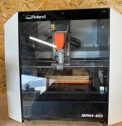
Some informations of the device, CNC SRM-20
The device used to mill boards in my lab is a CNC Roland SRM-20.
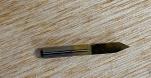
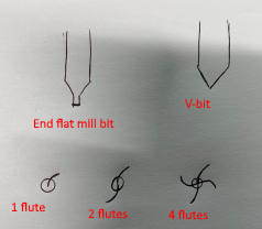
To mill in electronic, there is different tools. One of the tool is a milling end flat bit, the tip of the tool is at the same size. It is flat at the end because it is not really go through with milling the material at the tip but on the size of the tool.
Another tool is a V-bit, the is not the same size along the tip of the tool.
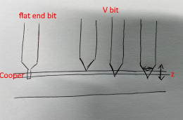
The board is made of copper, copper is conductive. The goal of electronic board is to make electric connection but not everywhere, the connection has to be between two points. With a end mill the tool can go down on the copper, it will have the same size. The V-mill size of cut depends on how depth we go with the tool, the depth is called z. That’s why the v-bit has to have an extremely precision with z.
At the end of the end mill, there is two kind of teeth, called flute. There is many kind of tool with different flutes.
We cut PCB material. For Fabacademy we use FR1 because it is a less strength material and easier to mill, and we solder with hand the end, hand soldering. The FR4 with epoxy is more for industry, and there they solder with oven. FR4 is more resistant for electronic board outside, and last longer too.
On the device, there is the bed of cnc, a sacrificial layer, some glue and finally the FR1 board.
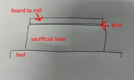
We never mill the bed because the surface where the mill occurs has to be perfectly flat to mill, so we put a sacrificial layer. We glue the board with double face tape, it is the fixture. On the board we do the traces and then cut the all shape. When we do the final cut of the piece, we go a little bit down, on the sacrificial bed to cut well.
One of the purpose of the week is to figure out how small can we do the track on the board, and how fine can it be in between two traces.
The board need to be as flat as possible because we will mill micron. We put tape, there can be air bublles than wont make the material flat. So we put the tape behind the board, the flattest as possible. There is dust on the sacrifial part, I have to clean everything before stick the board on it. Then peel the other part of the tape, position and press. I have to press it hard to be sure it is fully glued. It has to be really well glued but not too much to be able to remove the material after the cut.
When the door of the device is open there is protection, some buttons can not be clicked for the safety. To switch on the device, press three seconds on the switch on off button.
The using of mods
We use mods to transform a png file into a file that can be read by the cnc software.
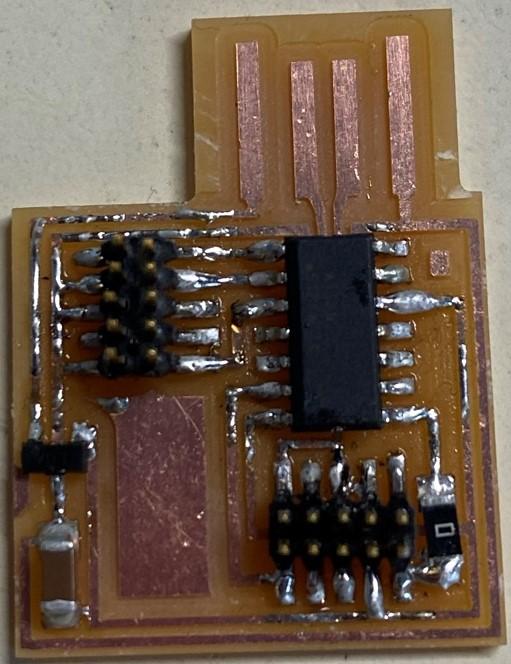
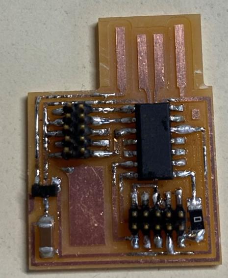
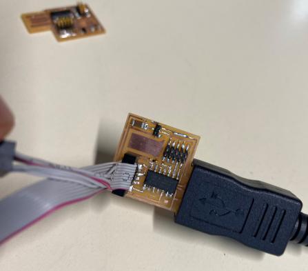
First we mill and then stuff the board (solder the components). I was said to do a JTAG programmer board with 10 pin. JTAG are able to control microcontroller that are cheaper and more powerful. The microcontroller of this board is D11C.
In circuit programmer, hardware is the files. In the fabacademy website in programmers there is files, traces and outlines, this is pictures, we have to transform them in order for the device to be able to read.
In mods :
Programs > open server program Srm 20 is the one we have, then pcb png because we want to mill png file.
There is boxes we can move, there are numbers and buttons, it is one way of building a program.
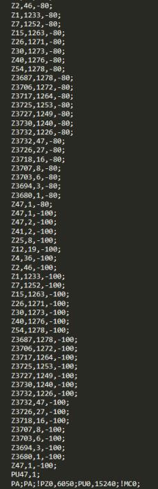
Here are the step I followed to create the .rml file, the format that the software can read. I cut in climb. Climb
For the traces :
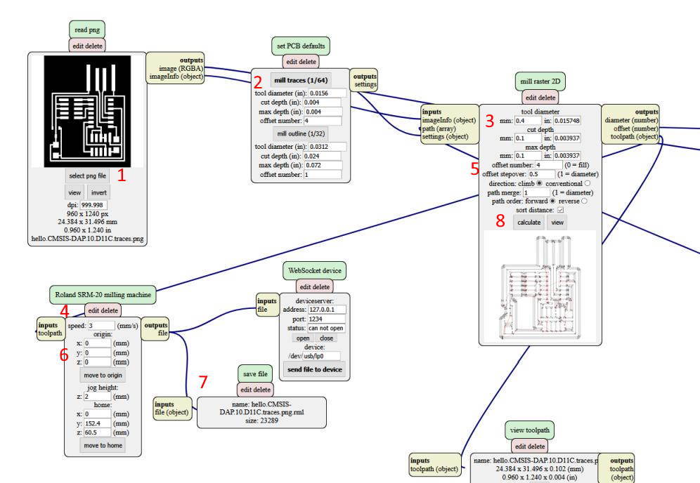
- Select png file (1)
- Select mill traces (2)
- Change the tool diameter (0. 4 mm), how deep we want to cut copper (0.1 mm), and max depth (0.1 mm) (3)
- Find the correct speed (3 mm/s) (4)
- Offset number is 4 here. The offset number is how many time we do the outlines of the traces. The max depth and the cut depth are equal to the same number, it means that the tool will not dig inside the board but will only stay on one value of z axe. We need to remove outlines of traces for them to not stick together and have gaps between the traces. (5)
- Origin is the zero point (6)
- The output is to save file (select (save file)) in the programmer (7), and click on calculate (8)
- The device software is .rml
- We can see a 3D shape, and where the tool go
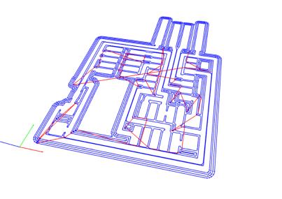
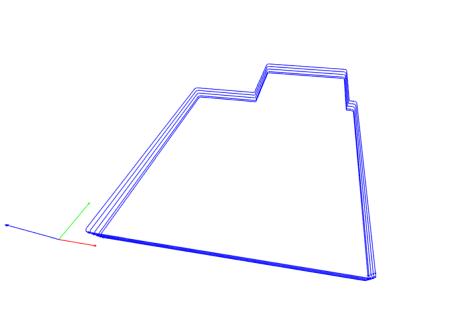
When we calculate the browser opens a window to have a preview. The blue lines are the path the tool will follow and the red lines are the movements the too will do. We can see that the shape is flat, the tool will only doo the outlines of the traces.
I need to add a box to save my file
- Right click > modules > open server module > file > save
- Connect the box to the ouput > file
- link file to file
For the outlines :
Right click > program > program server > srm-20 > png
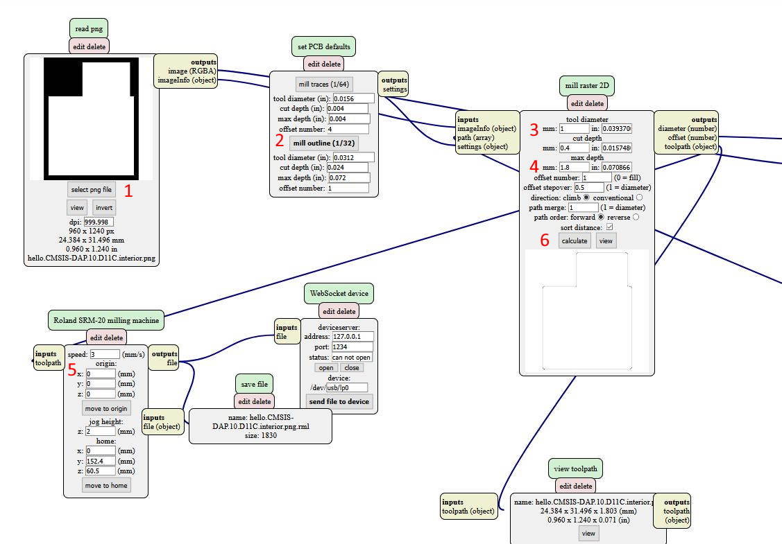
- Select the file for the outline (1)
- Mill outline (2)
- We will use 1.0 mm tool, I want to cut the thickness of a FR1 board (3)
- Max depth is 1.8 mm and cut depth is each deepness cut 0.4 mm. The max depth is the thickness of the PCB board. To cut totally the board, we can’t do it directly because we would break the tool. That’s why we will pass many time on the same line with going a little deeper everytime (here 0. 4 mmm) to cut the shape step by step. (4)
- We cut only 1 time, the offset number, we cut only one path.
- Then the speed is 3 mm/s and set the origin again 0 0 0 (5)
- Calculate and it shows the file and save it (6)
On the preview, we can see that the shape is in 3D, the tool will cut and dig through the PCB, and will do it 5 times, each step for 0.4 mm and will adjust the last path.
At the end I have two files because it is two different operations. All the values were given by my instructor.
The software to use the machine, V panel
V panel is the software we us for the SRM-20 Roland. It do not editing at all, it just make move and read files.
X Y Z are moving with the arrows (1), we can move continue or by measure (x100 = 1 mm). There is some position. Click XY button make x and y the zero (3). For the z don’t do it in continue mode. We play with x100 x10 and x1 (2).
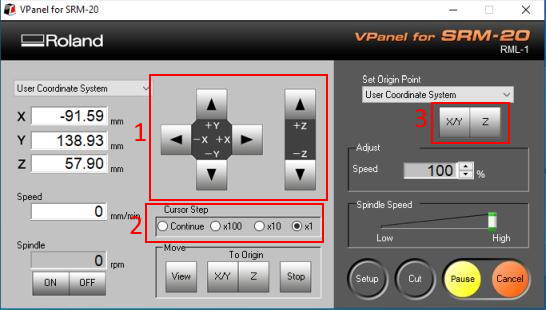
We do the z with the multimeter in the continuity mode, to test the conductivity.
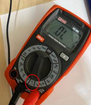
So I touch the plate with one tool and plug the crocodile clip on the milling bit. We it rings we click on z and it make the zero. When it rings it means that electrcity go through the to end and the tool is touching the board.
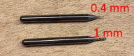
The 1 mm bit is to cut, the 0.4 mm bit is to do the traces.
We will make tests with differents bits.
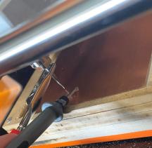
We insert the bit inside the collet.
To change the bit, I hold it with a finger to avoid the falling otherwise it would break. I screw and unscrew to remove the tool.
The door of the device has to be close to start the spindle.
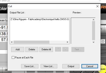
To launch a file click on cut. Add the file, select it and click on output, it will start directly.
Mill of boards
So I have my files, I can start the milling of my boards
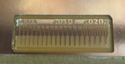
The test board
So first I did a board for the group assignment, to test a tool. I choose a 0.4 mm tool with 1 flute. You can find here the differences between a 0.4 mm bit with 1 flute and 0.4 mm bit with 2 flutes.
Here is the file of the traces of the test board.
Here is the file of the outlines of the test board.
Credits: these two files comes from the fabacademy website for electronic production
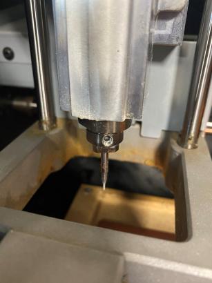
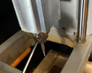
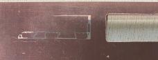
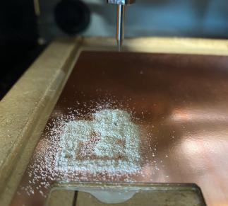
First one of my teammate already stuck a board on the sacrificial layer in the device, so I wanted to use it but it wasn’t flat at all. We can see that the board is not flat because the tool cut only on one side but when it go to the other side it is not cutting. That means that the z is different depending on the side.
I had the idea to remove it, remove the tape and stick it again but when I removed it and remove the tape, but lots of little bits of tapes stayed stuck on the back of the board. So if I wanted to stick again tape it wont be flat.
I took another FR1 board. Then I relaunch my file but as you can see on the picture, the board it still not flat. I measured the z at different places on the board and the z was not the same.
I added some micrometers in the z to go deeper. To do that I put the tool next to the board, outside the board, and set a new z on the software.
I finally reached the right cut but when I wanted to cut the shape, it didn’t go enough deeper. So I add some deepth with the z and cut again but it appear that the cut was not at the same place, even if I didn’t touch the x and y. The sacrificial and the bed layer had moved, it had to be tighten again.
I checked on the .rml file the values and I might have set the depth wrong because it only go until 1 mm. That’s why the shape wasn’t cut. I opened the file .rml with a text editor. On each line the value on the right is the deepness of where the tool is going. Indeed, the tool is not going further -100 (-1 mm)
To fix that problem I get down the bit for 0.8 mm.
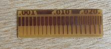
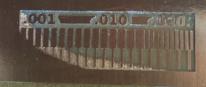
So we can see that an 0.4 mm bit with 1 flute milled here a FR1 PCB. It can mill the traces from 0.004 inch (0.1016 mm) and it can do a gap between to copper lines from 0.016 inch (0.4064 mm).
The programmer board
Here is the file of the traces.
Credits: this image comes from the fabacademy website for programming
Here is the file of the outlines of the board.
Credits: this image comes from the fabacademy website for programming
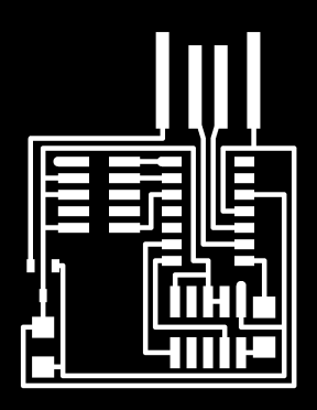
Here is an image to help for where the components will be.
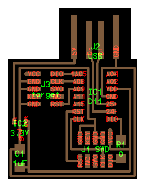
Credits: this image comes from the fabacademy website for programming
And here is the final result that have to be reached.
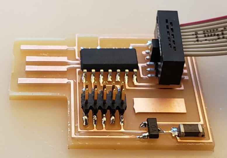
Credits: this image comes from the fabacademy website for programming
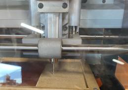
After milling the test board, I did the programmer board. I made the board on the same FR1 sheet I did the test board, so a not very flat board. I started the mill of the board but I set the z on the deepest point of the shape, and when the tool comes to a part with a bigger thickness, the tool broke.
I had to think to a way to mill my board without breaking a tool. To avoid that I milled the board by step. First I milled the lower part of the board and then I launched again the file to mill the upper part. Maybe I could have decreased the speed of the tool.
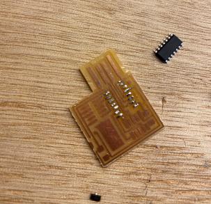
At the end I finally succeed to cut my board.
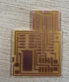
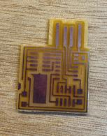
I need to remove the copper in the USB shape.
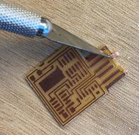
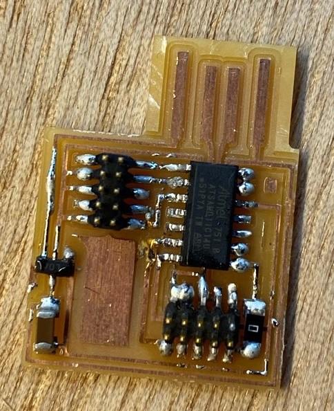
And here is the final result of the board without stuff.
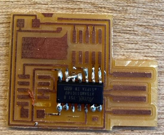
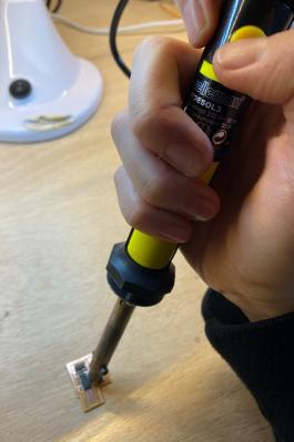
Now I am able to start the soldering. To solder the components I need to go from the center to the outside of the board. I started with the microcontroller but it was not ok, I need to practise the soldering but for now, the legs of the components are touching. I soldered in first the microcontroller but it is a big component and I burnt it a little bit when I soldered the smaller components. I made an other mistake, I warm too much the traces and it unstick the copper from the board. I will check at the end if it is still working.
To remove the excess of tin I use a desoldering pump that warms. To use it I place the end of the pump next to the tin I want to remove.
And when it is melted. I push the button to suck the tin.
Wenn all the components are soldered on the board, I checked with the multimeter if the current go through the traces and the legs of the component.
And it did everywhere, so the board is working.
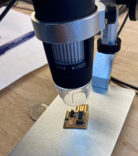
I also checked the soldering with a microscope connected to my computer if all the tin links were good.
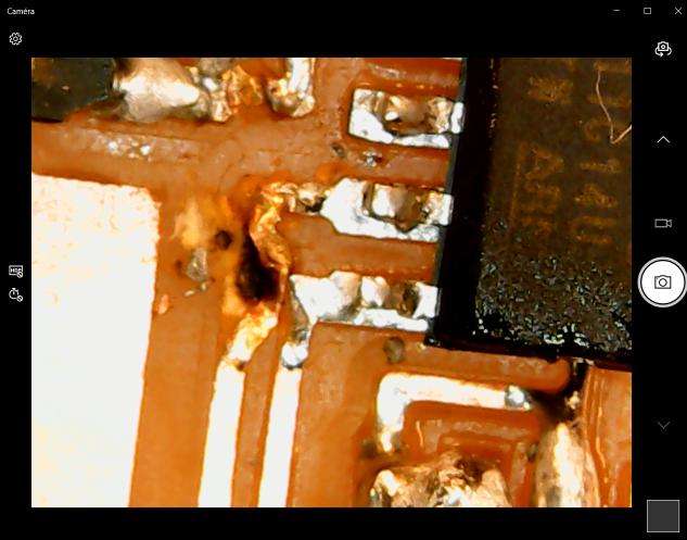
We can see the traces burnt by the desoldering warm pump. I wasn’t really happy of the result because there were heaps of tins and burnt traces so I did again the board. I kind of tin the board before the soldering to see if my components would stick better to the board and it did.
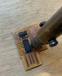
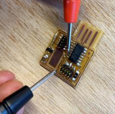
Here again I put too much tin for the soldering but to remove it I didn’t want to use the warm pump because before it burnt my traces. I used a desoldering braid and it worked so much better.
To use the braid I put it on the solder I want to remove, warm it with the solder iron and remove the brain. In my opinion, it does a nice soldering and it is easy to remove for me.
Flash the programmer
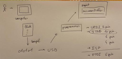
For what I understood now, the goal of a programmer is to make the link between the microcontroller of the electronic board of my project and the computer. The human is writting code on the computer, for example make a light blink. This code is then compiled in a language that can be understood by the microcontroller, like 0 and 1. The microcontroller in the project board has only the function of controlling the project, not to speak to the computer, that’s why a programmer is needed. The programmer has the function of transmitting the message between the computer and the project’s board with the microcontroller
On the programmer board, there is some pins, that make the link, with a cable between boards with microcontroller. The programmer understand oonly one language with only one kind of pin. The UPDI, with 2 PIN, JTAG, with 4, 6 or 10 PIN, ISP, that is an old language and FTDI, with 6 PIN, that is not really a programmer language but still.
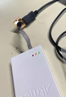
To flash the programmer, I need to tell him that he is a programmer. To do this I use a programmer that can be bought in a store. Here I am using an Atmel Ice programmer. My computer works with Windows operating system, that means that my computer needs a software to see the programmer plug. I need to download Microship Studio for my programmer to be able to talk to the computer (or the opposite).
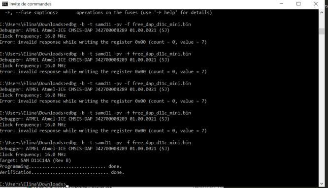
Then I have to download EDBG to write the command line that will flash my programmer. I download the latest verion for windows, then rename the .exe file as “edbg.exe” to be able to use the command line.
edbg -b -t target_type -pv -f binary_file
Using edbg means that I will be able to read the programmer from store (or any programmers) that will itself read the programmer board.
I could use my .exe file like that but I would have to change the “edbg” in the command line. Then the target is samd11, it is the name of the microchip. The binary file is given. Here is the file free_dap_d11c_mini.bin. The file has to be on the same directory as the edbg.exe file.
So now, plug everything on the computer. When the programmer from the store is plugged to the computer it makes a red light, then plug it to programmer electronic board. On this board the programmer from the store has to be plugged in the 10’s pins in the continuity of the USB key. The other pins are to program an other board with this programmer. Then plug the USB key of the programmer to an electrical source, for exemple, the computer. And when it is done, the programmer from the store make a green light.
Now that everything is plugged, I can execute the code line.
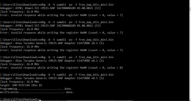
edbg -b -t samd11 -pv -f free_dap_d11c_mini.bin
I used the second board I made, these without the burning trace, but it didn’t work. I plugged the programmer in the other side but it sill don’t work. I realized that when I soldered, I linked two traces that are supposed to be not linked.
I have to desolder it. I took my other board and launch the code, and now it is working.
It means that my programmer board is now a real programmer, I can program other board with it.
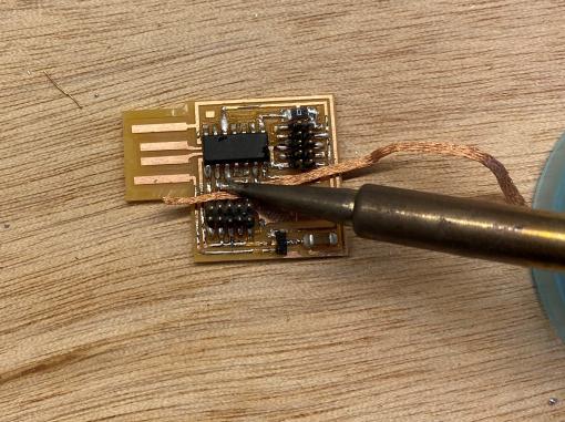
The goal is to make the second board a programmer too. I desolder the wrong stuff, add some tapes behind to make them fit in a USB plug well, without gaps.
To link my two boards I need to build a cable that can fit with the 10 pins plug. To do it I cut a piece of cable, put on the black plugs and press on them.
I did the same as before, plug everything, and execute the line code. The “burnt traces board” has became my programmer and the cleaner board is the board which is programmed. I have to try every side of plugging between the two boards and it finally worked. Now my two boards are programmers.
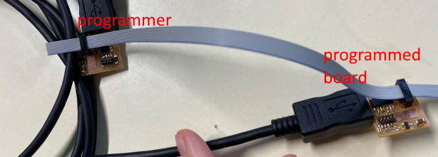
So at the end of this week I built my own programmer, that I will use in my final project to make the link between the code on my computer and the electronic board for my project.
All the files
- traces of programmer board
- outlines of programmer board
- traces of the test board
- the outlines of the test board