7. Electronics design
2nd week dedicated to electronics, after the production which was very interesting place for the desig board. In the documentation that will follow you will discover all the steps to make a board. That’s why I decided to choose KiCAD to design my board.
Use the test equipment in your lab to observe the operation of a microcontroller circuit board (in minimum, check operating voltage on the board with multimeter or voltmeter and use oscilloscope to check noise of operating voltage and interpret a data signal)

Document your work (in a group or individually)
• Individual assignment:
Redraw one of the echo hello-world boards or something equivalent, add (at least) a button and LED (with current-limiting resistor) or equivalent input and output, check the design rules, make it, test it.
Hero Shot
Workfow
- Download KiCAD
- Choose a board on the FabAcademy website
- Download and import the component library for KiCAD
- Create your personal board on KiCAD
- Export svg files
- Go to mods to create the G-code
- Preparing your board and milling your board
- Collecting all your components
- Soldering your components
- Testing continuity
- Flash your board using your microcontroller
- Download Arduino and the MattairTecht package
- Connect your board to a USB port on your computer.
- Select your communication port in Arduino
- Upload your modified code to your board
Individual assignment
In order to carry out the exercise ask who was to redesign a board and by adding a button and an LED I decided to take the “hello.D11C.serial.5V”. This board seems complex to me because there are two power circuits (3.3V and 5V) but these characteristics will surely be useful for my final project.
KiCAD
To redesign a board I decided to take KiCAD. This software is open-source, therefore free and well known in the industry. Moreover after use I find it easy to understand and use even for beginners like me.
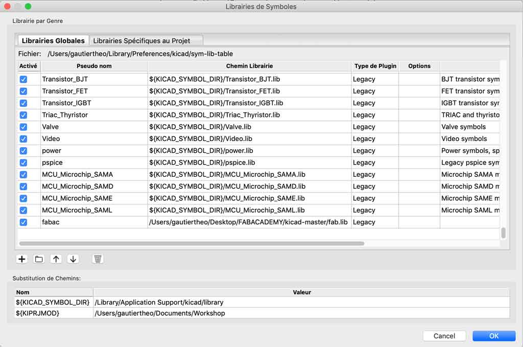
Installation of the library
Before you start drawing the board you need to download KiCAD and the FabAcademy library here. To do this you need to download a compressed folder and then decompress it. Once these steps have been carried out, the link between KiCAD and the downloadable footprints and symbols folders must be set up. To do this, go to :
KiCAD > Preferences > Configure the symbol library > Click on + > Choose a name for your library > Add the path to the folder
Same thing for the footprints library except that this time you have to choose “configure the footprints library”.
Creating a board
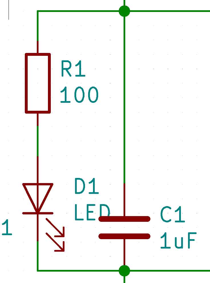
In order to create a board, several components must be inserted and connected to each other. In order to show you how to use KiCAD I will make a very simple electrical circuit. I will only insert a LED with a resistor for the power and ground sources. If you want to make a more complicated schematic you will just have to insert more components but the logic remains the same.
Eeschema
| Step | Illustrations |
|---|---|
| Open KiCAD and create a new project, for the example I called it “Documentation”. |  |
| Open the “eeschema” application to create the electrical diagram of your board. |  |
| When you get to this application you have to insert your components, to do this click on the “place symbol” icon and then click on the grid. | 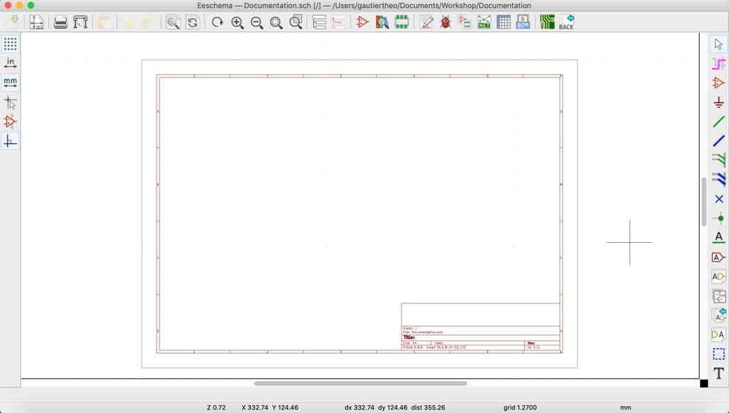 |
| The list of your components appears, you just have to select your component. | 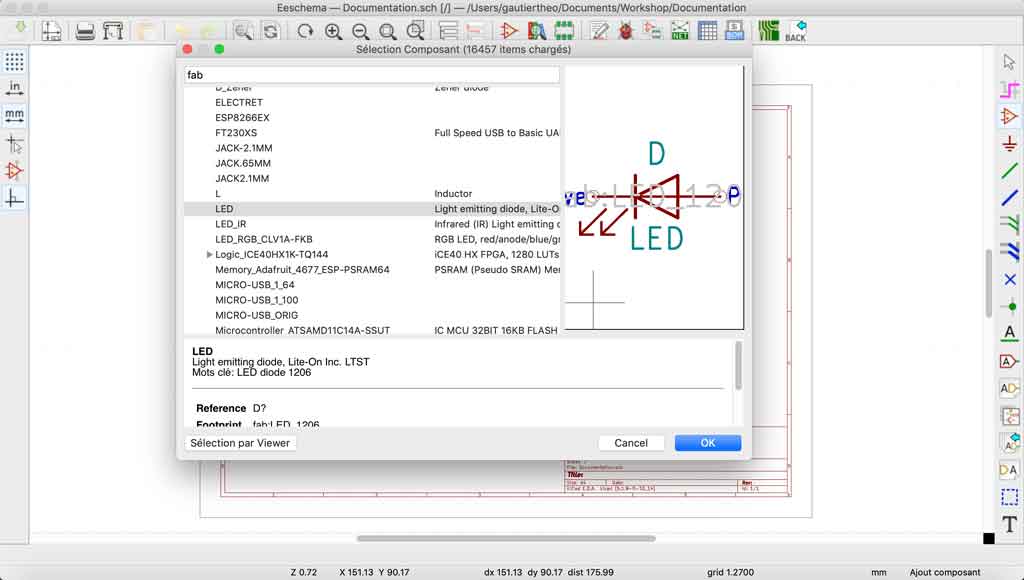 |
| Place your component where you want it and then click on your mouse (left click) to place it. You can rotate your component by pressing the “R” on your keyboard. I will then place a resistor. To do this, you have to perform the same steps, this time selecting the resistor. | 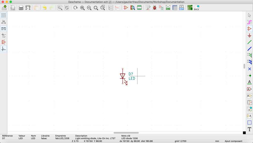 |
| I then want to add a power source, to do this click on the power icon (ground symbol) then click on the grid. | |
| Place your component where you want it and then click on your mouse (left click) to place it. You can rotate your component by pressing the R key. So I will place a ground. For that it is necessary to carry out the same stages while selecting this time the ground symbol | 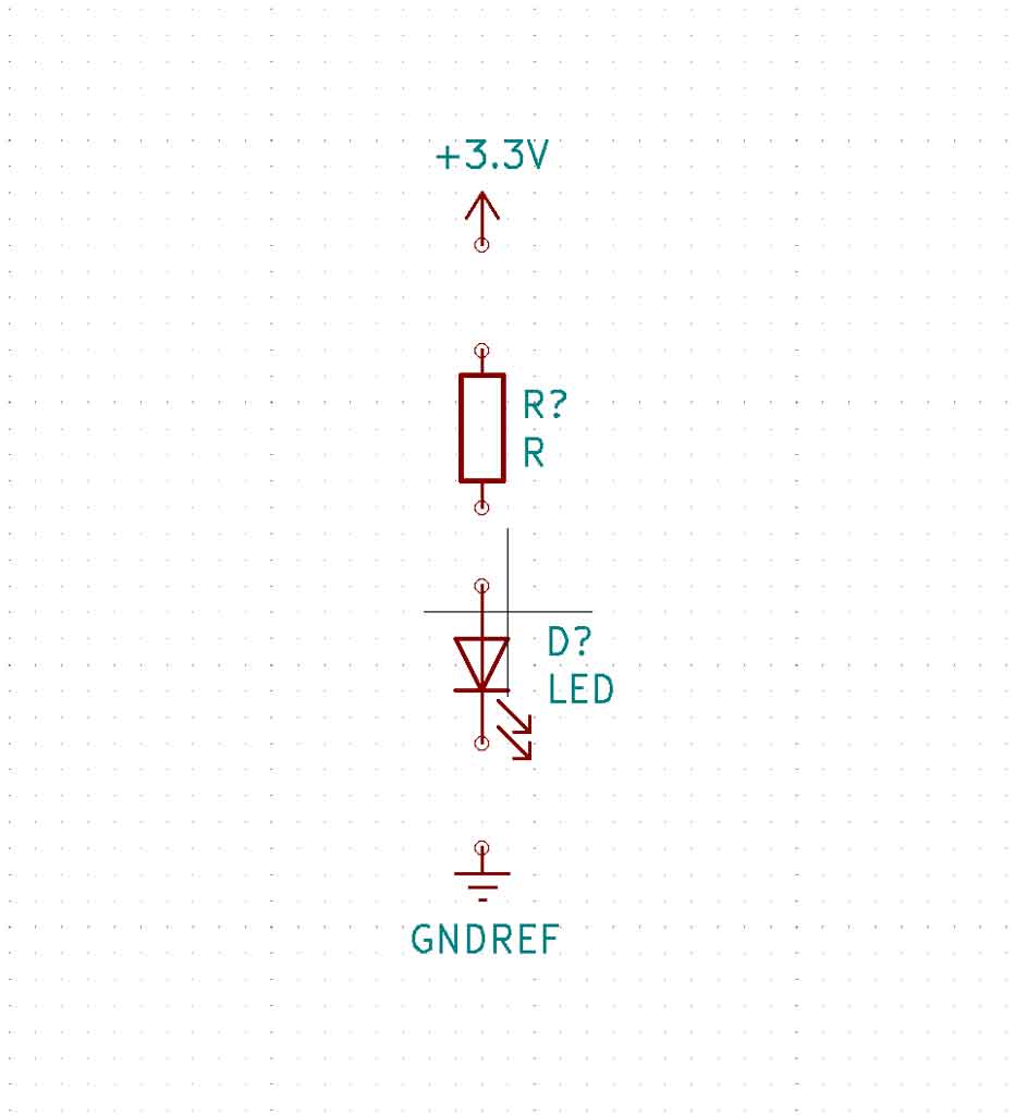 |
| Once all your components have been placed, you need to connect them with wires. To do this click on the wires icon and select the two points to be connected together. |  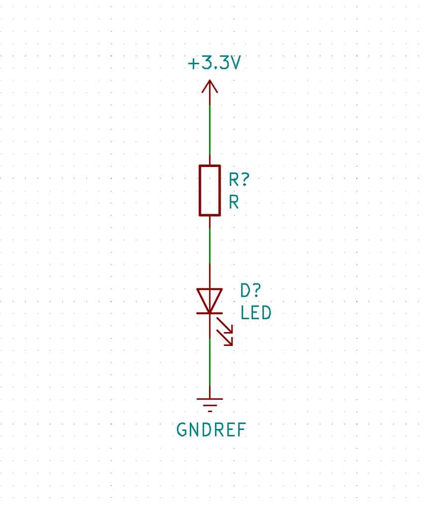 |
| You can name your components by double clicking on them. A window opens and you can modify the name but also edit its value. | 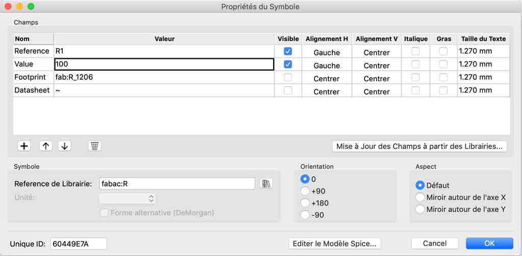 |
| Once you have completed your schema you can save it via the NetList application. |  |
| Register your NetList then open the “PcbNew” application. |  |
Sometimes footprints are not associated with the component. In this case you have to make a right click on the component, then property. Select the menu edit a footprints to match your component and your footprint.
PcbNews
| Step | Illustrations |
|---|---|
| Open the “PcbNew” application to make your tracks on the board. | 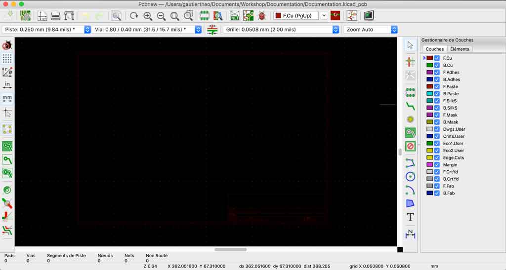 |
| Import your NetList : click on the NetList icon, select your file and then import the NetList.. | 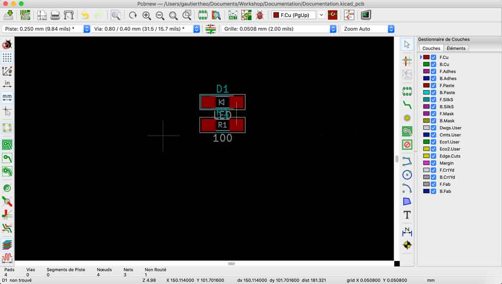 |
| Move your components, turn them to optimise your path | 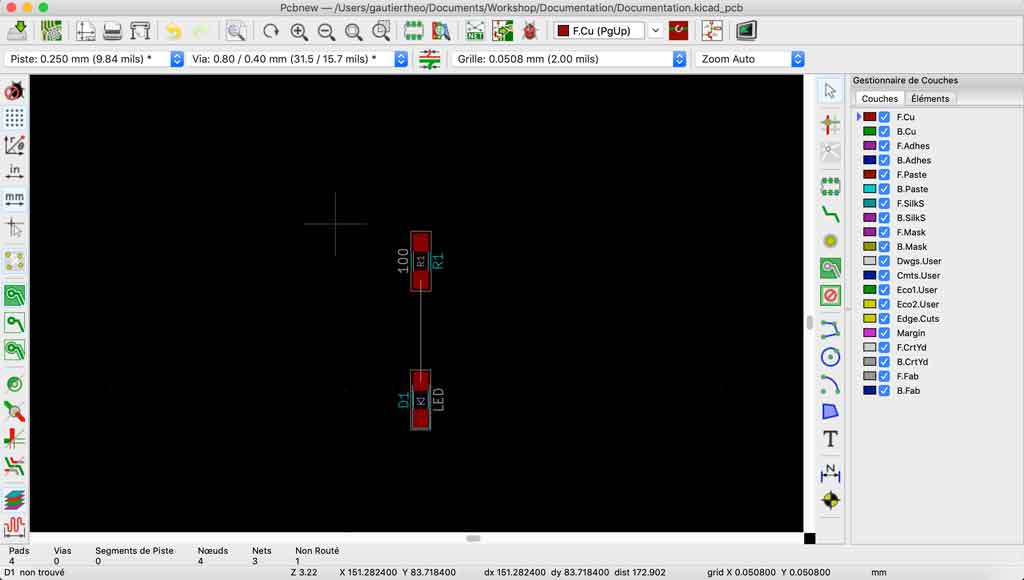 |
| To make the trace, select the “make a trace” tool and then select the two components to be connected. | 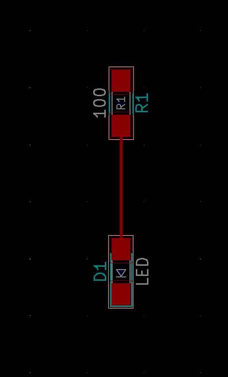 |
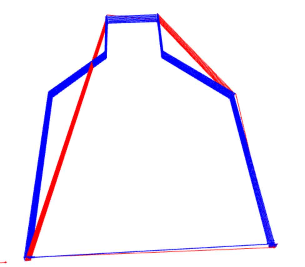
| Now that you have made your tracks, you need to make the location of your outside cut. To do this, select the “edge cut” layer and the polygon tool. |   |
| Design your exterior cut-out | 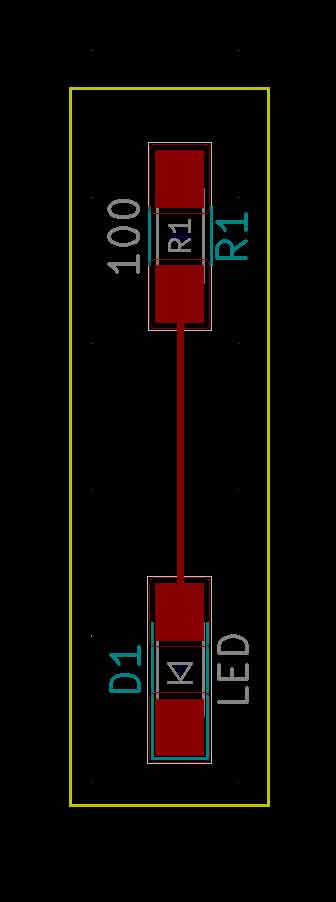 |
| You can now export your tracks and exterior cutout by clicking on File > Export > SVG | 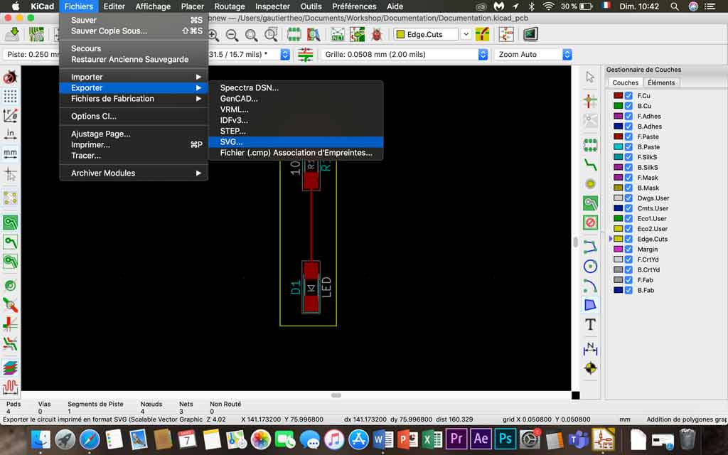 |
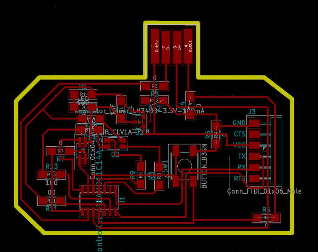
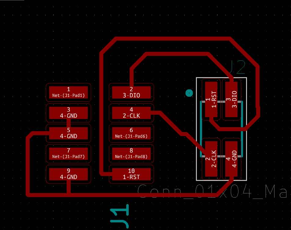
My board
Design with eeschema
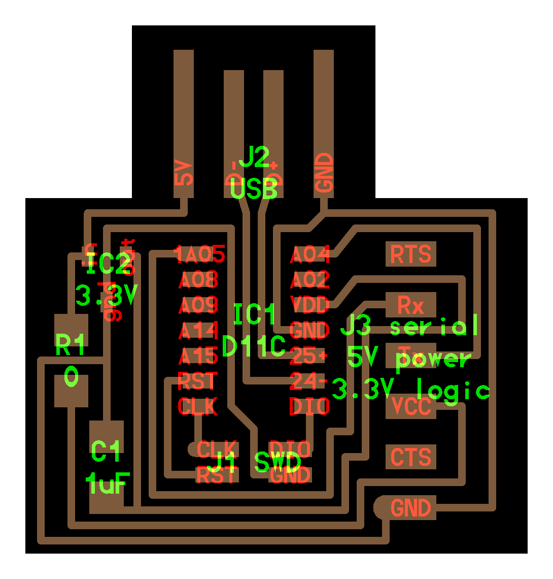
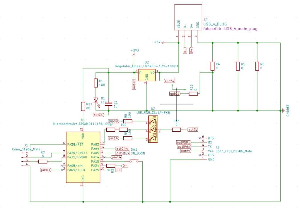
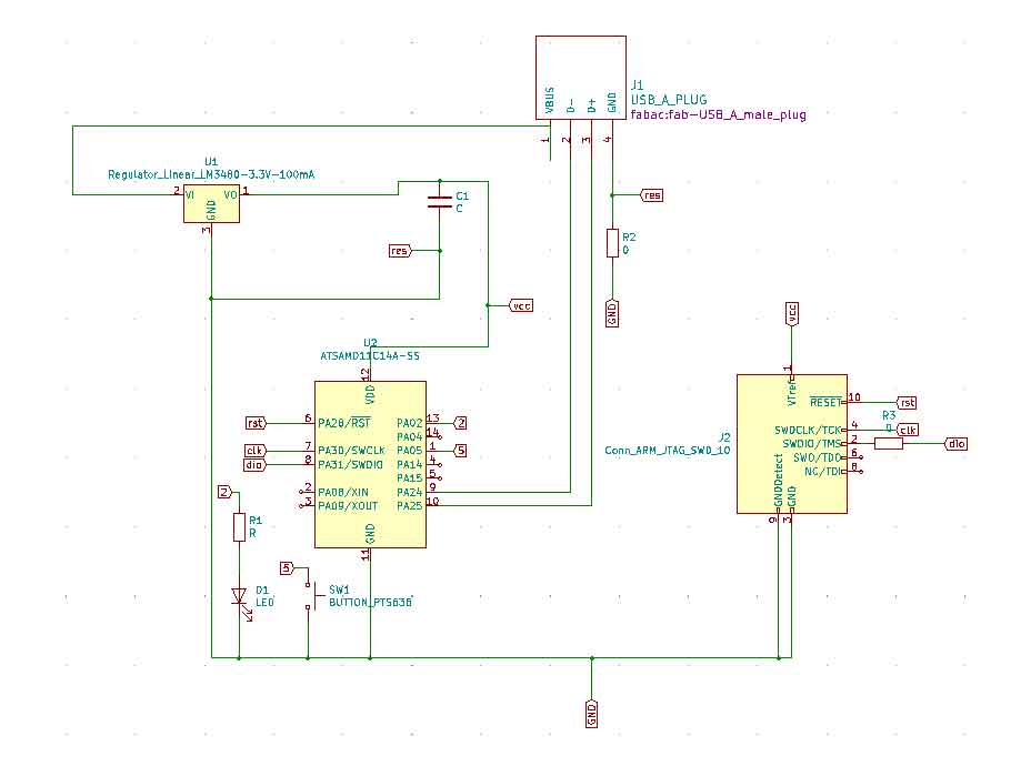
After taking a workshop on KiCAD with our instructor Luc I designed my board. As explained earlier I chose to take the “hello.D11C.serial.5V”. So I started to strictly copy the original board.
Then I added a green LED just after the transistor which allows me to see very quickly if my board is electrically powered.
In order to respond to the exercise ask I added a button on pin 5 of my microprocessor. I also added an RBG LED (LED that can make several colours by mixing the primary colours red, blue and green) which are controlled by pins 3, 13 and 4.

Global electrical schematic
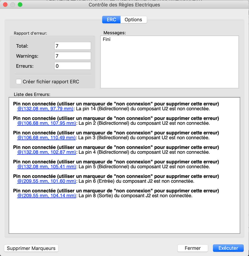
Design rules check
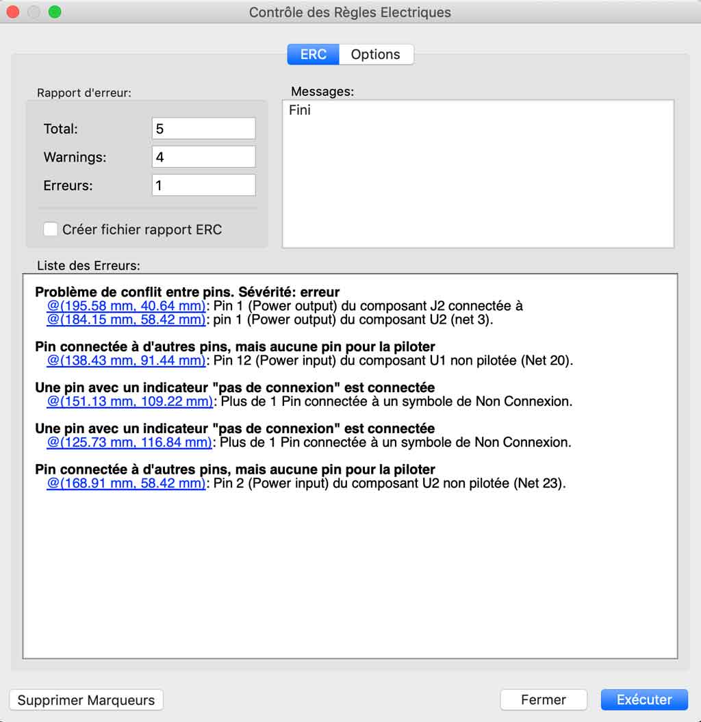
Checking the design rules I realised that I had a mistake and some warnings
Creation with PcbNew
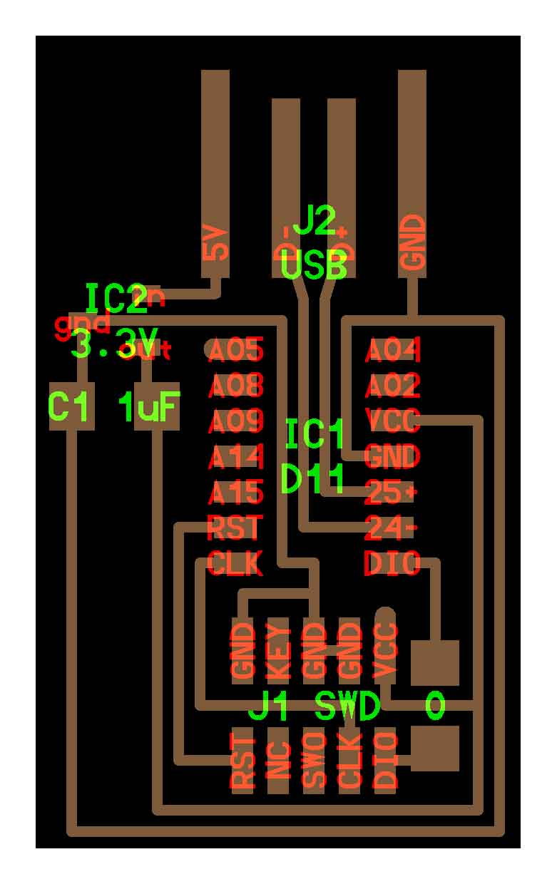
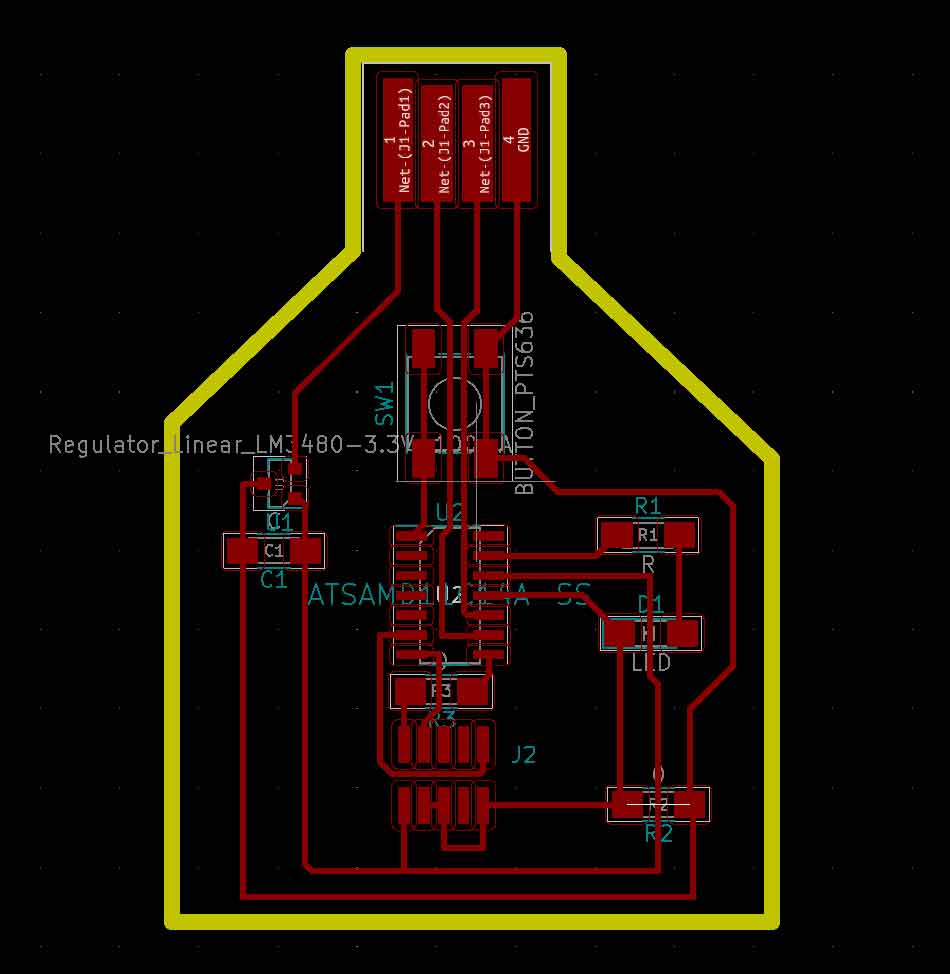
After finishing my electrical schematic I generated a NetList to import into PcbNew. First of all, I set the width of my track. For this I used the group tests we did a two weeks ago. So I set the width of the tracks to 0.4 mm with 0.2 mm of insulation on each side. With this I am sure that my bit can pass everywhere. After more than 3 hours of searching to find the shortest and best way I came to the following result. I am aware that the board could be smaller but caught in the heat of the action I couldn’t see the shortest paths. Also I use a lot of 0 resistance to jump off the tracks but I didn’t manage to do any better.
Why have so much 0 ohm resistance?
0 ohm resistors can be used to pass over a wire. Sometimes you have to connect two components together but you have a trace that blocks you from doing so. To do this, place a 0 ohm resistor and this will act as a bridge. You can then transmit the power to the other side.
When you have finish your own design you can export in svg to import it in Mods.
I then exported the file in .svg to be able to make the traces in mods. Here is the result after using mods. If you want more information on how to use mods I invite you to go to week 05 or click here.
/
Settings traces :
- Board : FR1
- Tool diameter : 0,4 mm
- Cut depth : 0,1 mm
- Max depth : 0,1
- Offset number : 4
- Direction : climb
- Speed : 3 mm/s
- Origin
- X : 0
- Y : 0
- Z : 0
Settings outline :
- Board : FR1
- Tool diameter : 1,0 mm
- Cut depth : 0,2 mm
- Max depth : 1,9
- Offset number : 1
- Direction : climb
- Speed : 3 mm/s
- Origin
- X : 0
- Y : 0
- Z : 0
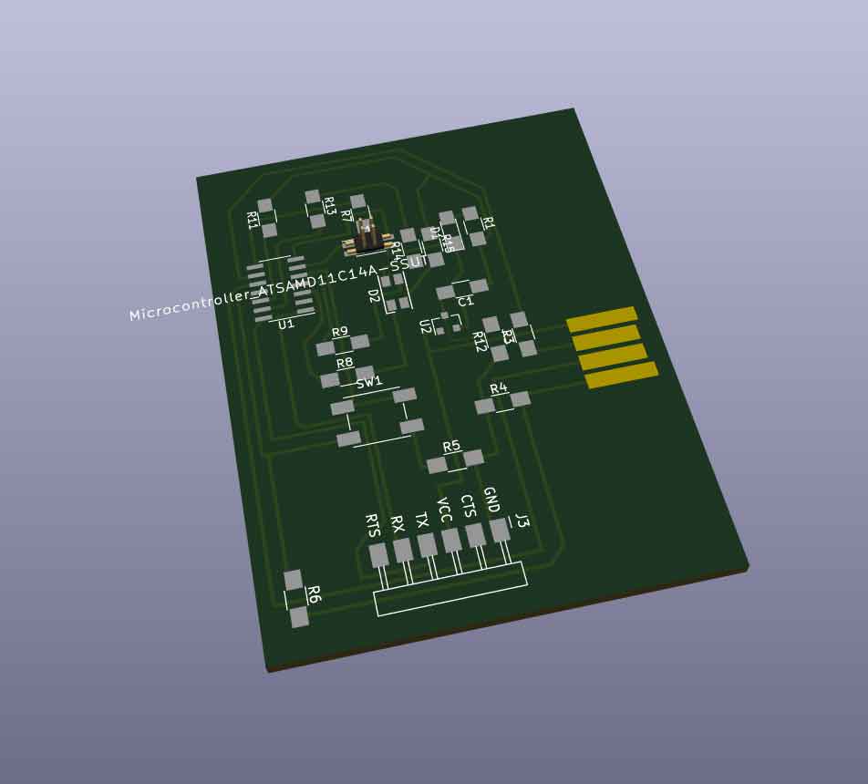
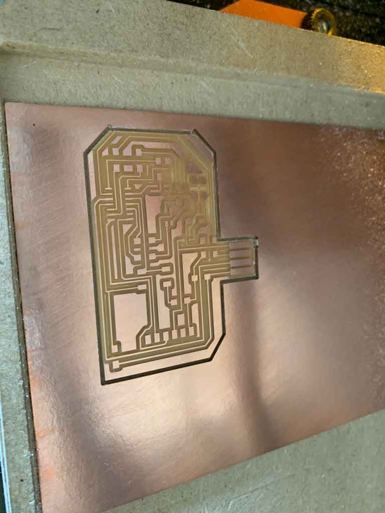
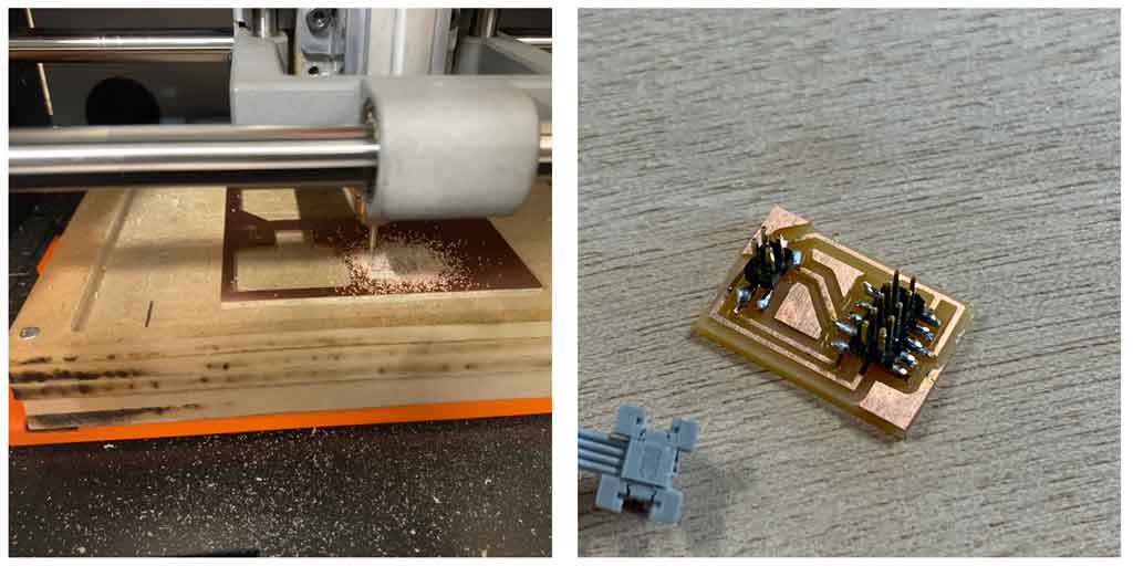
After more than 1 hour of cutting here is the final result
Soldering
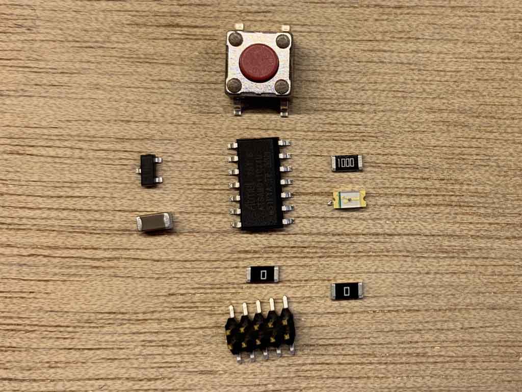
After the design and production step of the board, it is now necessary to solder them on the board. For this I used :
- 1 male connector 2x2 1,27mm
- 1 microcontroller SAMD11C
- 1 button 6mm
- 1 RGB LED
- 1 green LED
- 1 FTDI connector 01x06 male
- 1 capacitor 1 uF
- 1 regulator 3,3V 100 mA
- 4 resistors 100 ohm
- 9 resistors 0 ohm
 Thank you very much Antonio for the photos
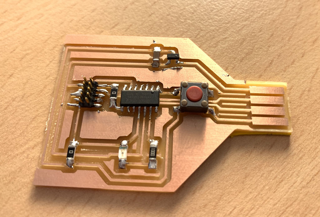
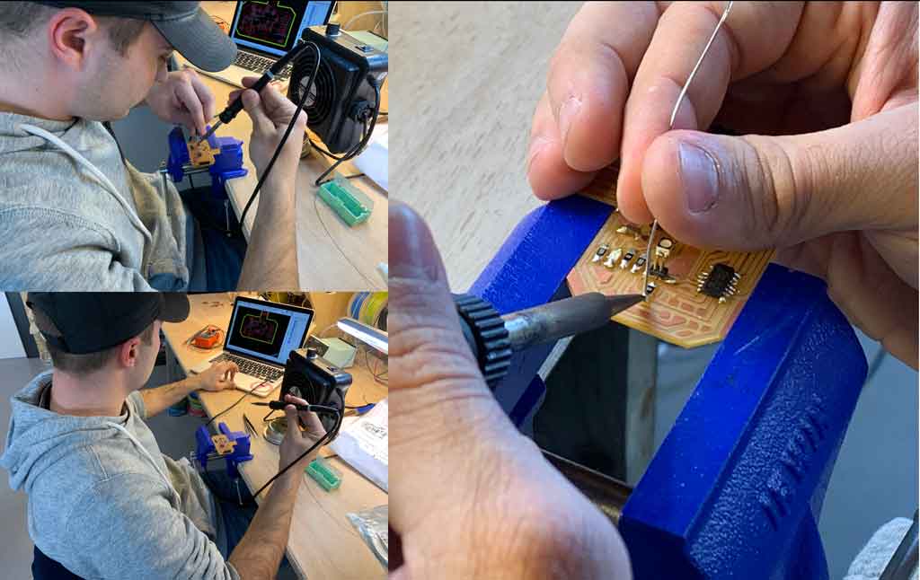
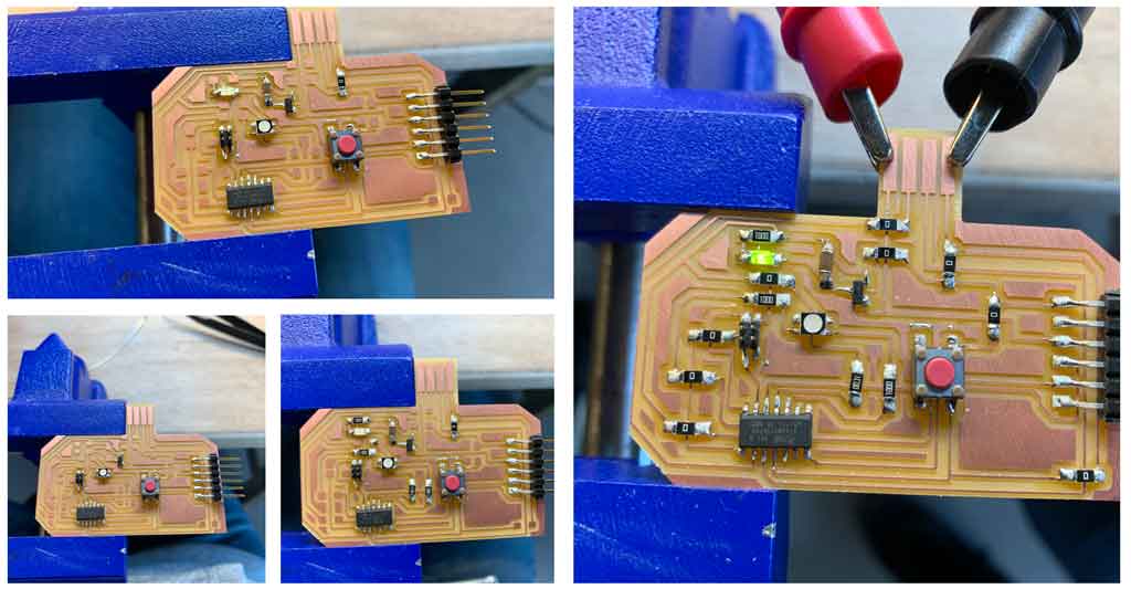
For the soldering I decided to solder the microprocessor first, then the 1.27 pins. Then I soldered the LEDs, then the button and the 2.54mm pins. Finally I placed the resistors, capacitor and transistor last. Here are the steps of the soldering.
Fabrication of the adapter
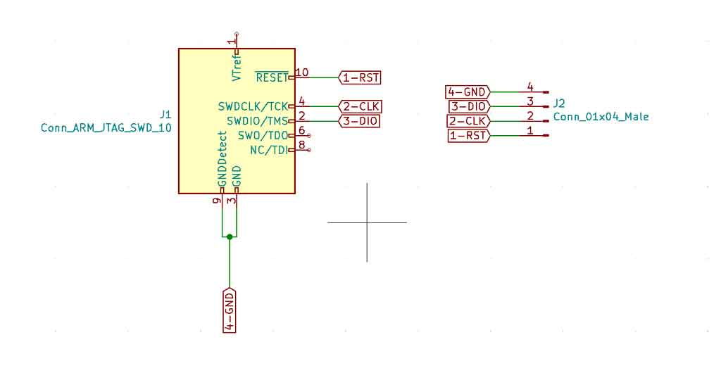
In order to be able to connect my board with my microprocessor I had to make a small adapter. My programmer is equipped with 10 pins 1.27mm while my new circuit is only equipped with 4 pins 1.27mm. So I made this small adapter.
Programming
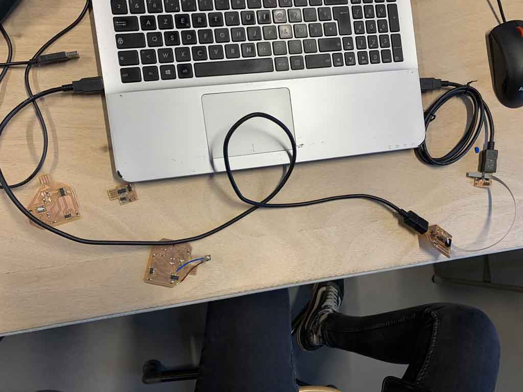
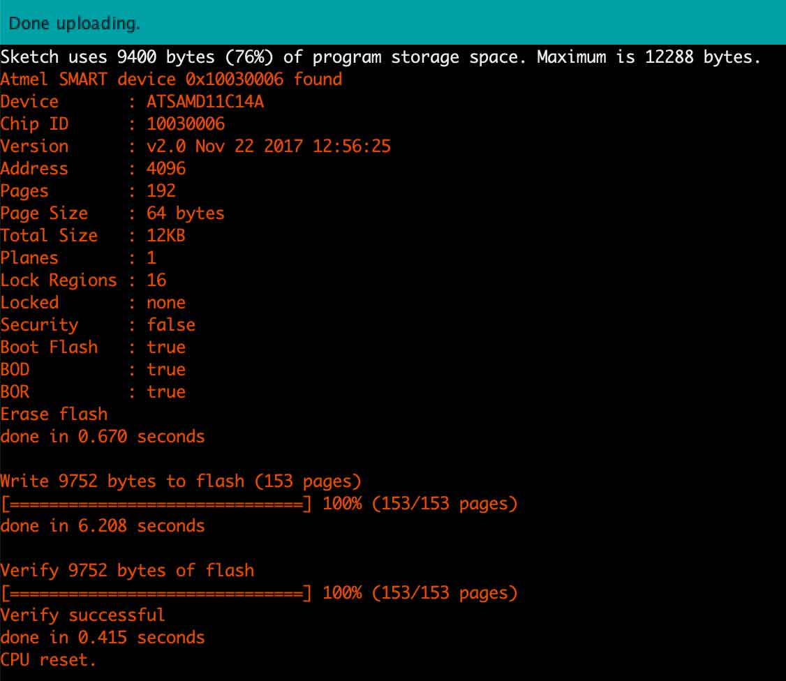
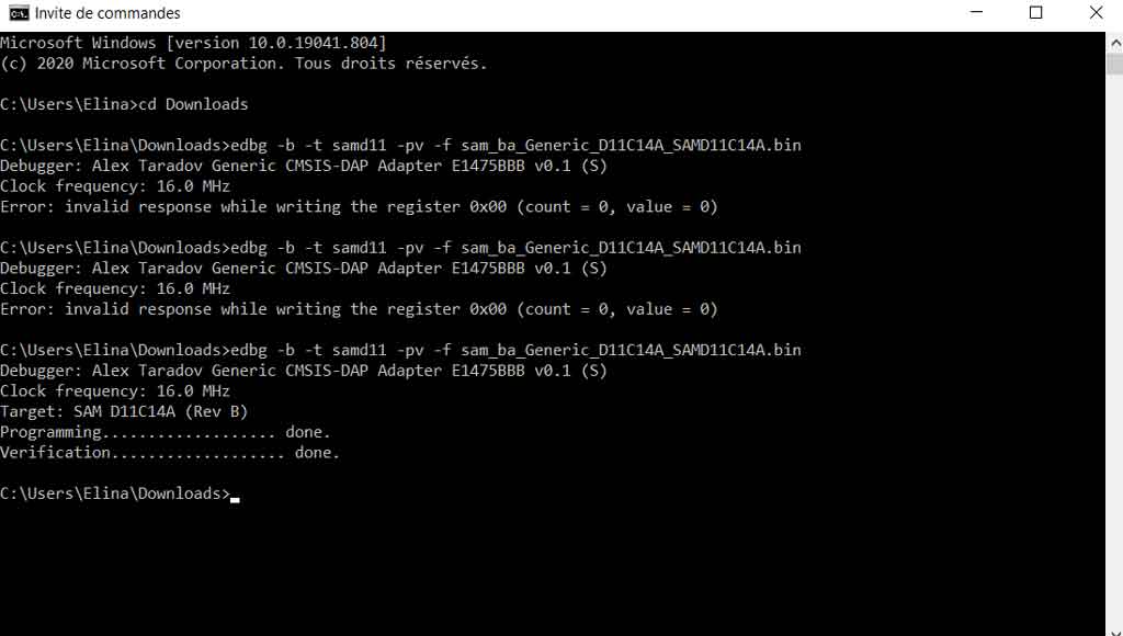
After Elina helped me to flash my board with the bootloader I used the Arduino application to flash my LED. Now that my board has the bootloader I don’t need the cables anymore, I can directly connect to the USB port.
First of all I need to download a pack so that the Arduino application can communicate with our SAMD11C microprocessor. To do this you need to copy this link and paste it into the preferences of the arduino application.
https://www.mattairtech.com/software/arduino/beta/package_MattairTech_index.json
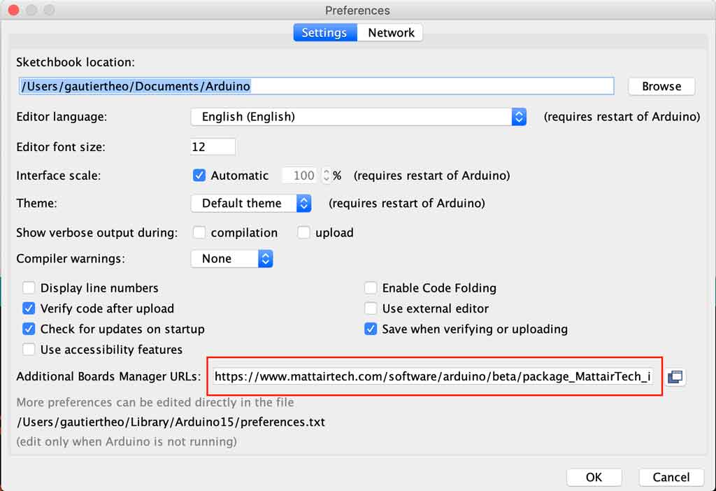
You can then go to tools then manage libraries to download the MattairTech library.
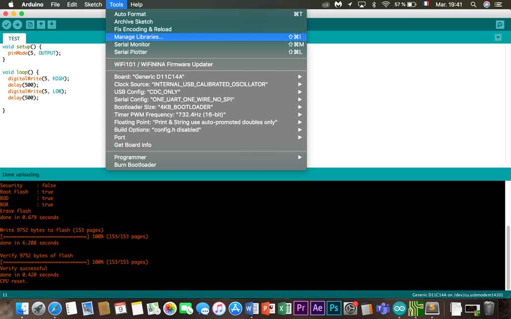
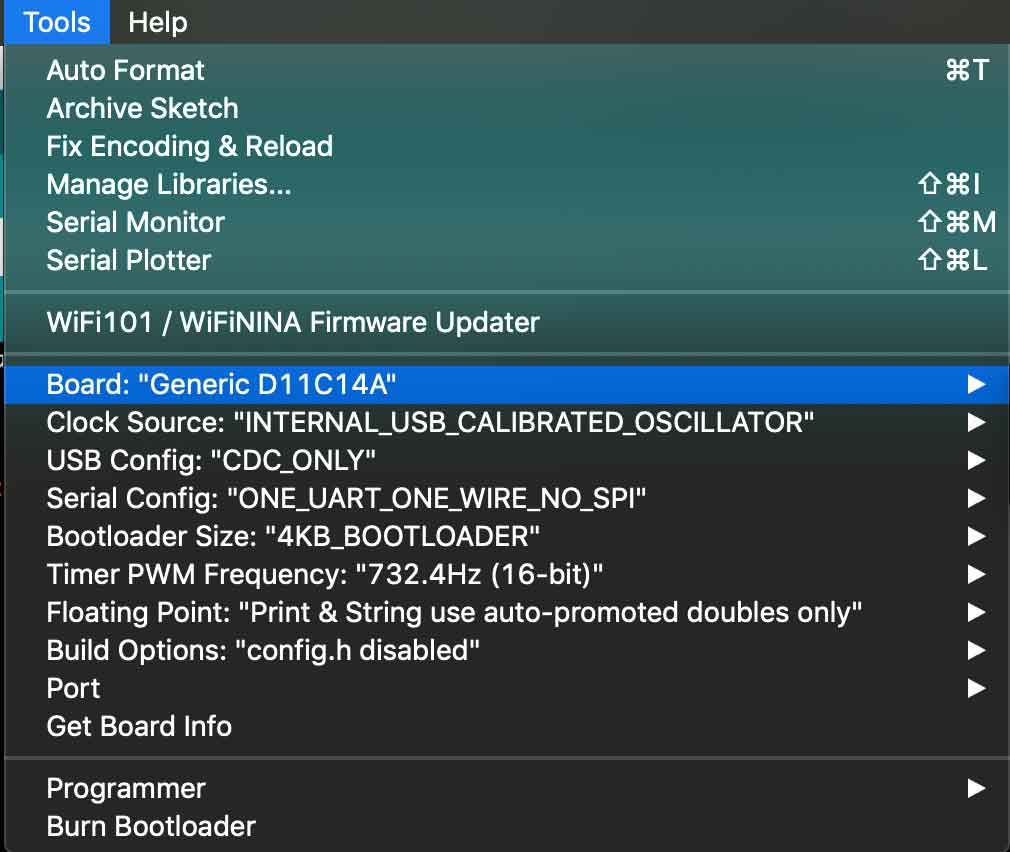
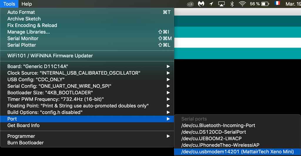
When you are ready you can connect your board to your computer via a USB port. Go back to Tools and select your board. You also need to select your USB communication port.
When you have selected everything you can send your code to your board. For my par I used the default code in arduino to generate my blinking. The only change I added is that I changed the pin out number to match my board. In order to know which number I used for this schema
``` void setup() { pinMode(5, OUTPUT); }
void loop() {
digitalWrite(5, HIGH);
delay(500);
digitalWrite(5, LOW);
delay(500);
} ``
Hero Shot
MistakeS
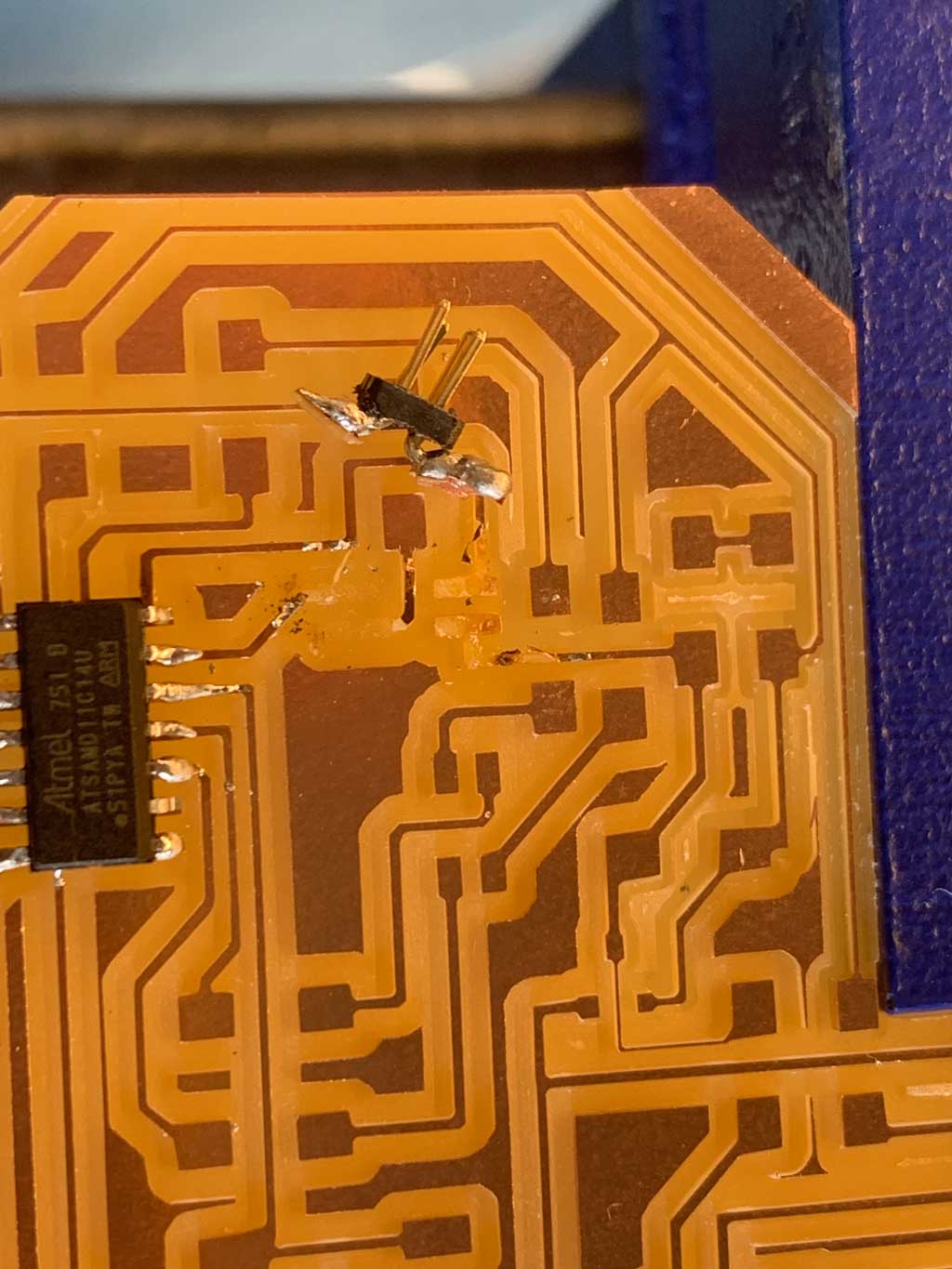
This week big disenchantment Monday morning. After having milled my board on Friday and prepared everything for Monday morning (components, soldering station, chair, lights…) I’m ready to go. Probably in too much of a rush because after soldering my microcontroller I wanted to solder my little 1.27mm pins. While doing this step I wanted (once soldering…) to move the pin which was crooked… big mistake, it totally ripped off my tracks. So I had to start a new board.
After I was soldering all my board and checking the continuity I decided to flash it to put the bootloader on it. Impossible to communicate with the board. I rechecked the schematic, the connections, turned the board around but nothing. So I decided to build a new board, this time very simple. I chose to use the “hello.D11C.echo” as my new board.
I had to start all over again from scratch. So I recreated the electrical schematic to add a LED and a button to the existing components.
I checked the design rules several times so as not to make a mistake again
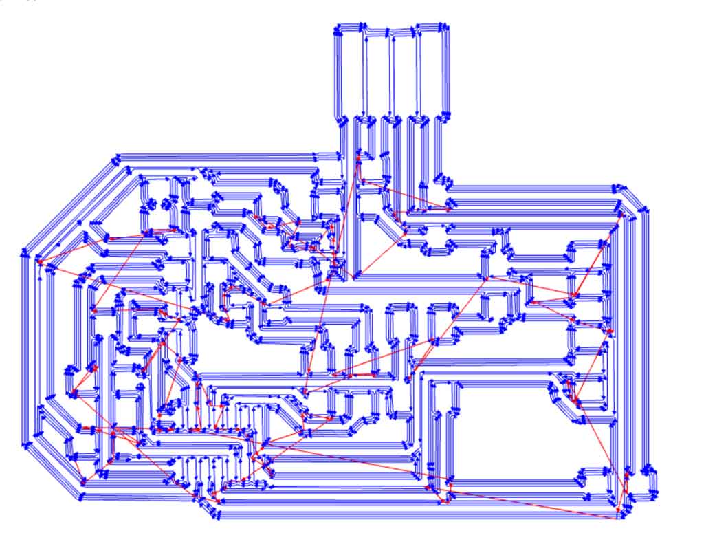
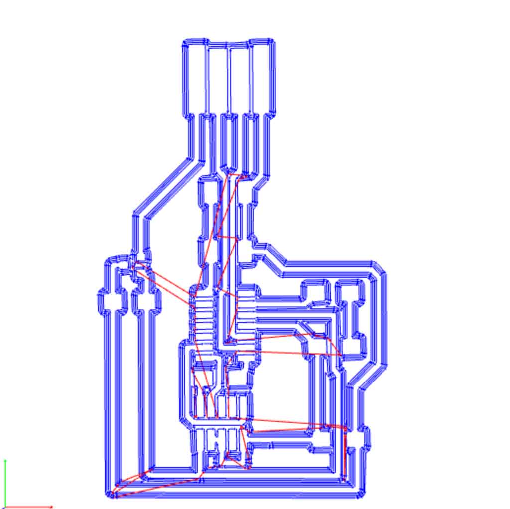
Then I had to start the tracks again as well. So I imported my NetList in PcbNew. Realize again the most optimal paths. Here is the result:
I then exported it in svg to be able to make the tracks in mods.
Settings traces :
- Board : FR1
- Tool diameter : 0,4 mm
- Cut depth : 0,1 mm
- Max depth : 0,1
- Offset number : 4
- Direction : climb
- Speed : 3 mm/s
- Origin
- X : 0
- Y : 0
- Z : 0
Settings outline :
- Board : FR1
- Tool diameter : 1,0 mm
- Cut depth : 0,2 mm
- Max depth : 1,9
- Offset number : 1
- Direction : climb
- Speed : 3 mm/s
- Origin
- X : 0
- Y : 0
- Z : 0
While the machine was making my board I prepared all the components I needed:
- 1 button 6mm
- 1 microcontroller SAMD11C
- 2 resistance 0 ohm
- 1 resistor 100 ohm
- 1 LED
- 1 capacitor
- 1 transistor 3.3V 100 mA
- 10 pins 1,27mm
I had to solder it again
My colleague Elina then helped me to flash my board. On my computer I couldn’t get my board to flash, she kindly offered to try it on her computer, it worked.
Group assignement
The multimeter
For the group assignment we used the multimeter to check the continuity of our traces but also to check the voltages at the terminals of our components. To do this we powered up Theo’s board and measured the voltage, continuity and resistor values at several points.
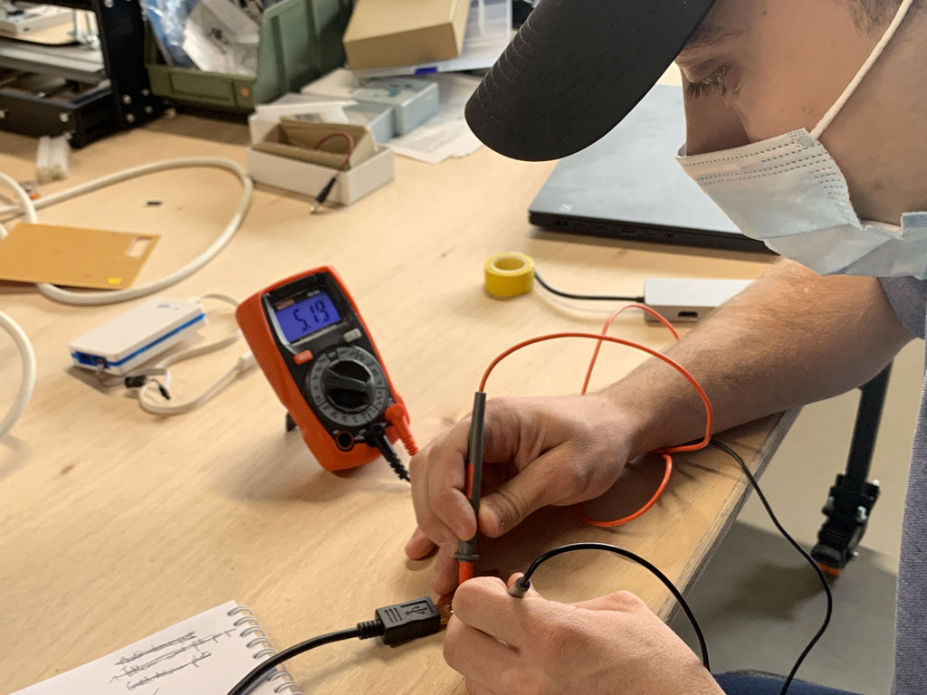
- USB terminal voltage: 5.19 V
- Transistor terminal voltage: 3.3 V
- LED terminal voltage: 1.73 V
- Measured resistance of the 100 ohm resistor: 100.1 ohm
- Measured resistance of 0 ohm resistor: 0.9 ohm
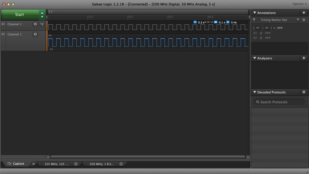
Logic Analyser
We also used a logic analyser to decode the signal sent to the LED. We understand better the functioning of the microcontroller with this tool