
Networking and communications
NETWORKING & COMMUNICATIONS
This is the content we had covered this week:
W13 - Networking & communications
- Purposes
- Wired
- Wireless
- OSI Layers
- Physical Media
- Modulation
- Channel sharing
- Errors
- Networking
Assignment
-
Group assignment: send a message between two projects
-
Individual assignment: Design, build, and connect wired or wireless node(s) with network or bus addresses
HOW TO USE NETWORKS
This week there was a lot of knowledge passed to us. It was too much to sketch it all, so I decided to diagram the parts I found more relatable for my project.
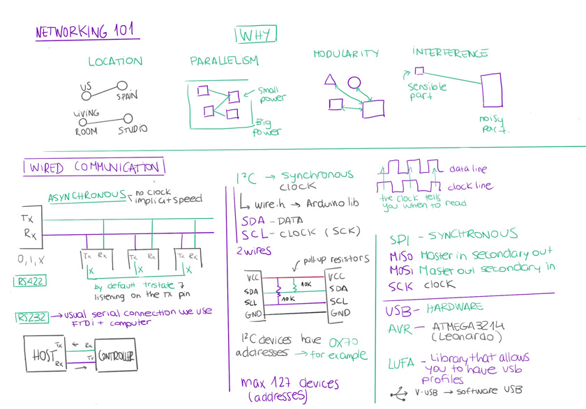
"Networks & wired communication."
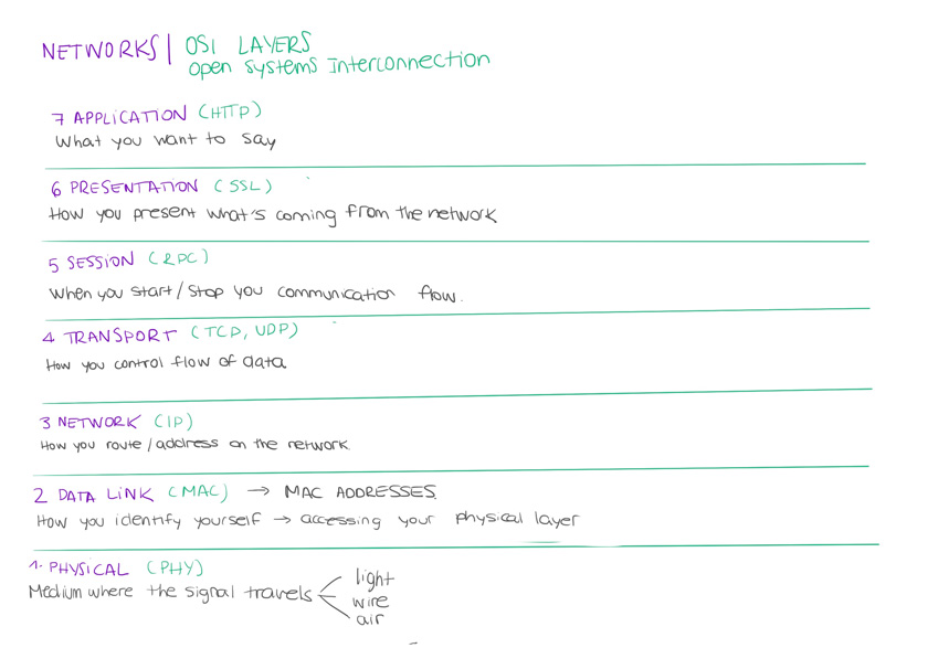
"OSI Layers Diagram."
GROUP ASSIGNMENT
As I’ve been working remotely this week I focused on the in class excerise that used I2C as I had multiple boards that could talk to each other. I didn’t have an ESP32 at hand so the second exercise I could do it, even though I was following the process closely.
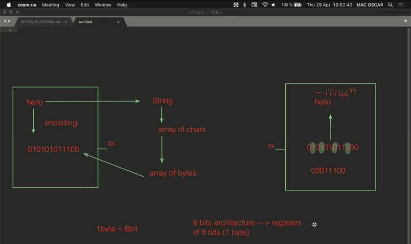
"Oscar's diagram explaining Serial comm."
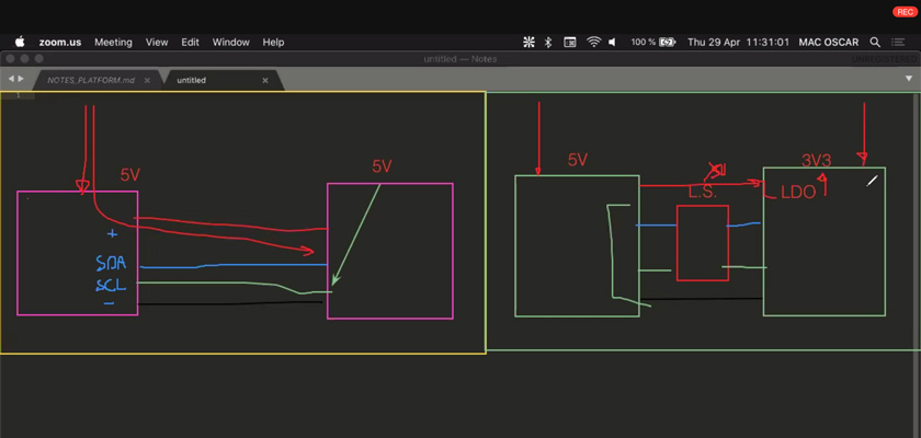
"Oscar's diagram explaining I2C comm. LEFT: same voltage devices. RIGHT: Different voltage devices with a Level shifter in between."
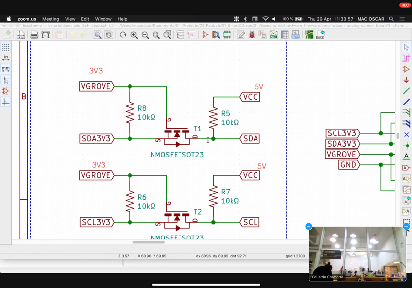
"Kicad Scheme showing pull-up resistors in between SDA and SCL wires."
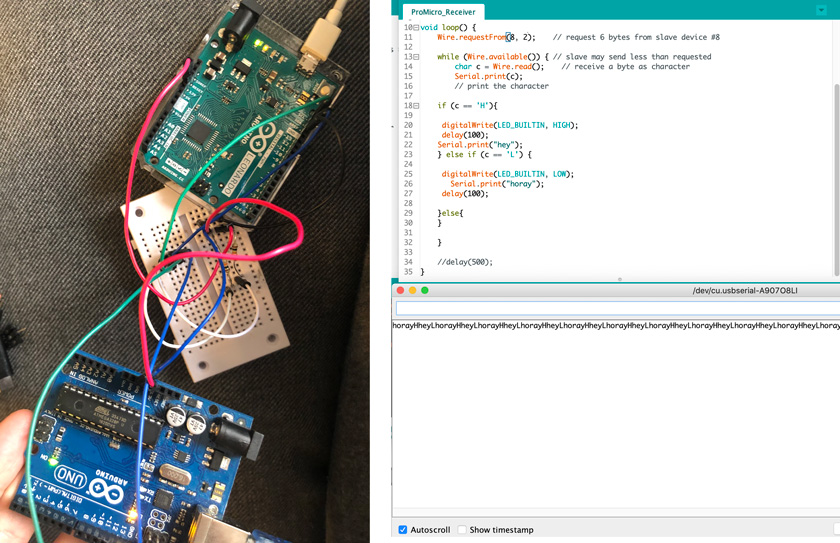
"LEFT: Arduino Leonardo & Arduino Uno connected via I2C. RIGHT: I2C receiver's code showing th serial port message underneath ."
Download Leonardo Sender I2C files
Download Arduino pro micro Receiver I2C files
WHAT WENT WELL
Better Understanding:The exercise was useful to incorporate something that should be part of my final project.
WHAT COULD BE BETTER
Too much theoretical info on the wireless side:I wish I had had more time to try things on wireless. I didn’t have time this week to do so. That’s a weakness for my future self.
INDIVIDUAL ASSIGNMENT
So this is the deal! My ( quite ambitious) final project requires many outputs and after talking to Edu and Josep on the final project review session I decided to try I2C communication. After a bit of research it seems that I’ll be maxing the I2C capabilities with a 100 devices. Will see how that goes.
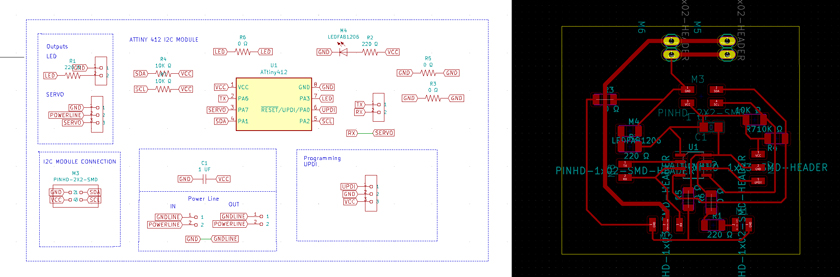
STEP 1: DESIGN NETWORK
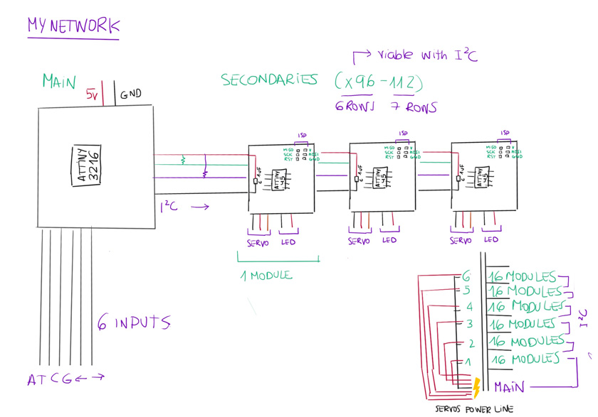
"Diagram showing my Networking proposal using I2C."
So this week, I decided to use as a main board the Tiny Outputs board I designed last week which already included wired SDA & SCL pins.
For the secondary board, the one that will control each individual servo I started from scratch trying to minimize all the elements I needed for both size and consumption.
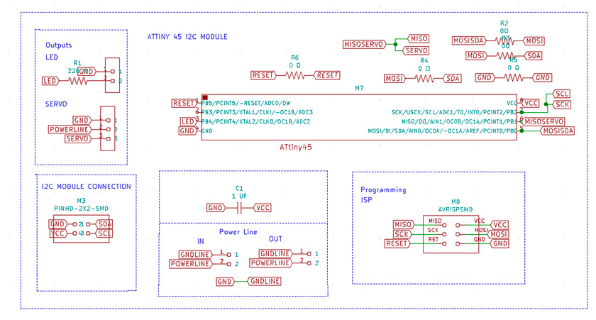
STEP 2: DESIGN SECONDARY BOARD USING KICAD | ATTINY 45
The sections that this board has are the ones that follow:
Powerline: There is a dedicated powerline (5V) to power the servos expecting them to draw certaing amount of current. This line goes in to the servo, and out to the next board’s servo. There is also power ( 5V ) + capacitor to power the board coming from the I2C connection.
ISP connection: to programm the boards. As I’m using an ATTINY45 to power the board, I need an ISP programmer ( Arduino ISP in my case).
Outputs: Servo (Ground, 5V & PWM) + LED (Ground + 5V).
In this case the elements I use for my secondary boards are pretty straightforward as a unit. The most important thing is to understand that multiple nodes will be connected one after the other using I2C. The Main board will also be connected to these nodes through I2C.
"Kicad scheme for my seconday board."
For this one, I decided to use Diego’s info to clean-out the surroundings of the board.
How to clean out the copper of your board by Diego
STEP 3: MILLING SECONDARY BOARD
PCB MILLING PROCESS: FROM KICAD TO THE END
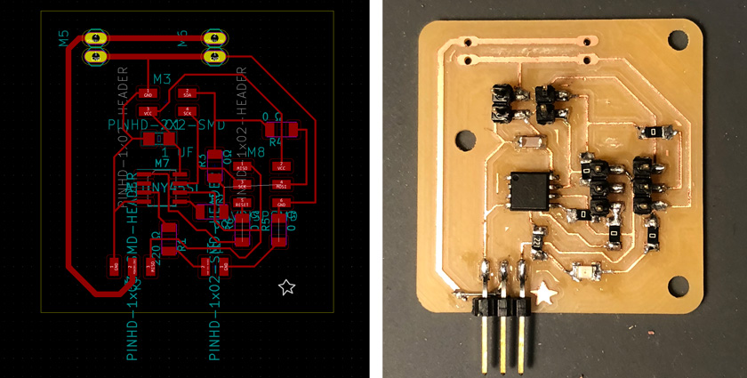
"LEFT: Kicad PCB with all components routed, ready to mill. RIGHT: Finished board number 1."
MILLING TRACES
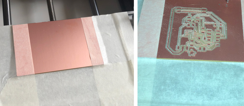
"LEFT: Copper Ready on the G-code cnc machine using Candle CNC. RIGHT: Traces Done usin 1/66 endmill"
To see the whole milling process go here
COPPER CLEAN OUT + HOLES + CUT
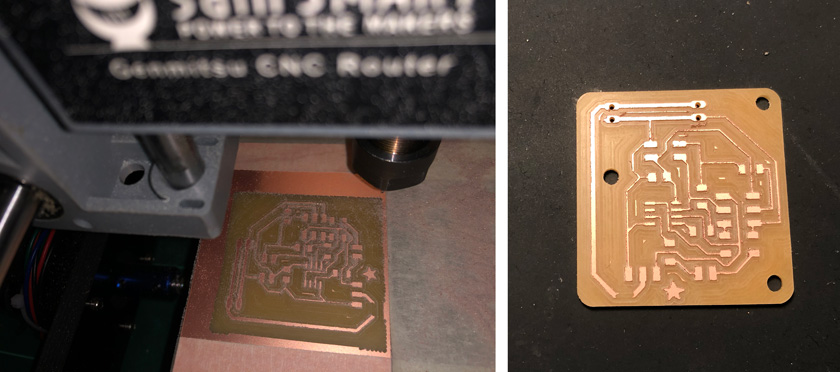
"LEFT: Copper clean out Done. RIGHT: Holes + Board cut Done."
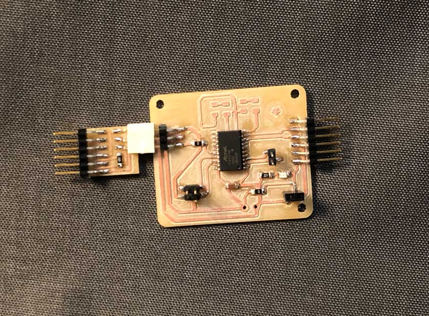
STEP 4: COMPONENTS ASSEMBLY
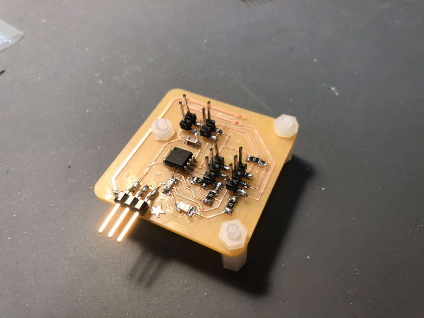
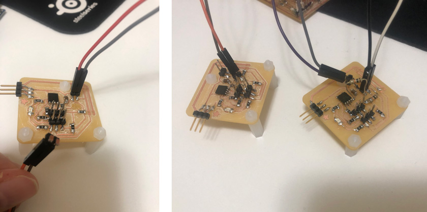
"Assembled secondary board 1"
STEP 5: ISP PROGRAMMING ATTINY 45 | USING ARDUINO ISP
"Arduino ISP programming setup for secondary board 1."
"Attiny 45 | Programming a simple blink using ISP to test board"
Download Blink code test for this ATTiny 45
STEP 6: TESTING I2C CODE WITH MY NETWORK BOARDS
FAAAAAAIL. Nothing seemed to work so I decided to debug things one by one: CODE, MAIN BOARD & SECONDARY BOARD.
STEP 6 BIS: TESTING I2C CODE WITH ARDUINO BOARDS
After trying to use the my boards I went to a controlled & stable setup and simplified the code as much as I could. This seem to work fine.
"Testing I2C code Arduino Leonardo + Pro mini"
Download Secondary Code Receiver
STEP 7: TESTING I2C USING ARDUINO LEONARDO AS SENDER & ATTINY 3216 BOARD AS RECEIVER
Then I thought that there might be something wrong with the SDA & SCL connection on my board.
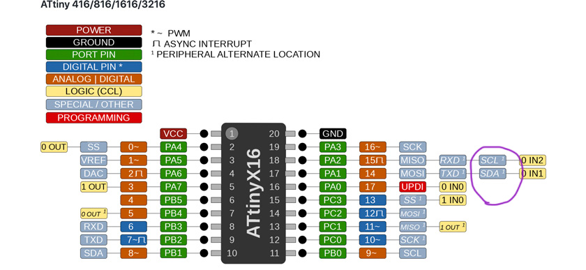
PROBLEM NUMBER 1: I’M USING THE SECONDARY PINS FOR SDA & SCL
When checking the wiring I saw that I was using the secodnary pins, and wasn’t really sure what that meant.
"Assembled secondary board 1"
Spence Konde MegaTinyCore Documentation for the rescue
This is the chunk of documentation that helped me to spot what I was doing wrong:
“Wire.swap(1) or Wire.swap(0) will set the the mapping to the alternate (1) or default (0) pins. It will return true if this is a valid option, and false if it is not (you don’t need to check this, but it may be useful during development). If an invalid option is specified, it will be set to the default one.”
"I2C Arduino Leonardo Sender + Attiny3216 board receiver"
STEP 8: TESTING I2C USING ATTINY 3216 BOARD AS SENDER & ARDUINO LEONARDO AS RECEIVER
" I2C Attiny3216 board Sender + Arduino Leonardo receiver"
STEP 9: TESTING I2C USING ARDUINO LEONARDO AS SENDER & ATTINY 45 BOARD AS RECEIVER
" I2C Arduino Leonardo Sender + Attiny45 board receiver"
STEP 10: TESTING I2C USING ATTINY 3216 BOARD AS SENDER & ATTINY 45 BOARD AS RECEIVER
"I2C Attiny 3216 Sender + Attiny45 board receiver"
STEP 11: TESTING I2C USING ATTINY 3216 BOARD AS SENDER & ATTINY 45 BOARD 2 + FIX AS RECEIVER
"I2C Attiny 3216 Sender + Attiny45 board 2 receiver (10k Ohm resistor fix)"
STEP INFINITE: RESOLDERING STUFF
"Kicad scheme for my seconday board."
WHAT WENT WELL
I2C might work:By having two modules that work independently I hope to make them work one after the other to test a larger network.
WHAT COULD BE BETTER
Delicate setup:There are many components that are quite brittle, and I don’t know why. I’m planning on reduing the board using more through-hole components that might be more sturdy, at least for pins + headers.
Might switch microcontroller:Programming with ISP ( using Arduino ISP) is a wire mess. If I need to program a 100 with this such error prone process I might stress out. I’m considering changing to Attiny412 or another inexpensive one to program using UPDI.
Frustrating debugging:This week there were so many things that could go wrong that it was very difficult to debug: from traces & pads breaking multiple times, SDA, SCL interferences,….
AFTER MATCH | TRYING TO MAKE THINGS BETTER
BEFORE STARTING AGAIN, I EVEN ATTEMPTED TO USE SOFTWARE SERIAL
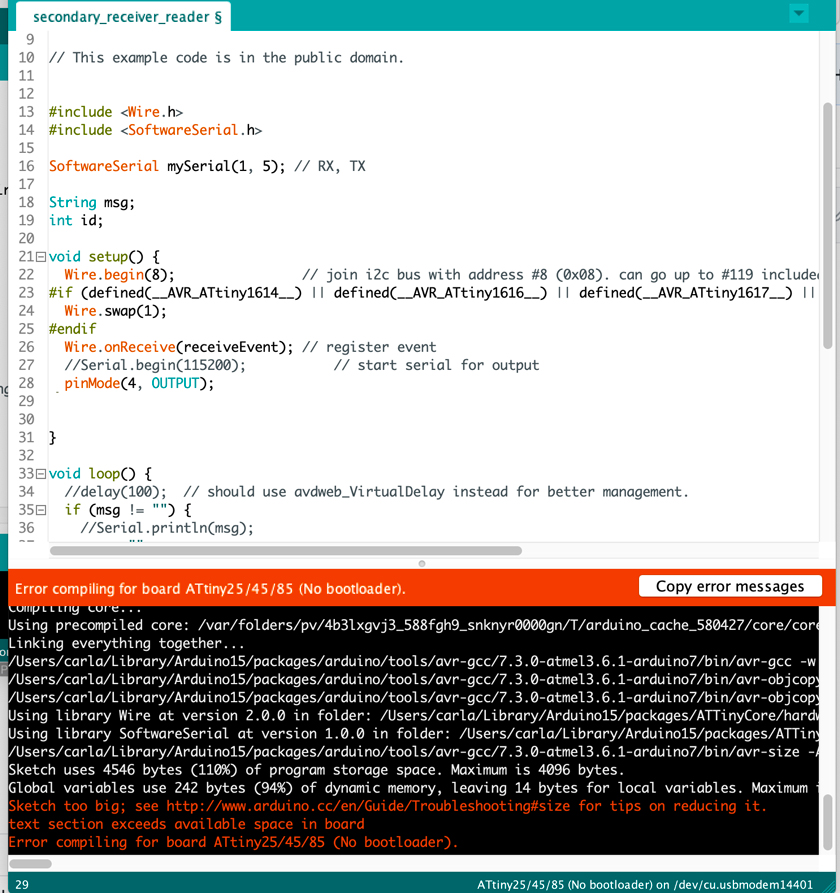
"Software serial too large for the ATTINY45."
I TRIED TO DESIGN A NEW NODE FOR THE 412
I was starting to be concerned that all the problems came from using the ATTINY45. Maybe the specs were too limited for my use case. I considered using the new AVR Tinys which have lots of wire libraries with less dependencies and even no buffers.
See this library the Edu sent us
Unfortunately it was a waste of time because I didn’t realize that we don’t have any new AVR microprocessor with this footprint at the lab when I went to mill it. I was a bit sad because I was looking forward to be able to program my “hundred” secondary boards using UPDI instead of ISP.
"Kicad scheme & pcb design for my seconday board using Attiny 412."
NEW MOVE, STARTING I2C CODE FROM STRATCH
After multiple days of frustration in which the code I was making would work in any commercial board but not my Attiny 45 I2C modules I decided to start the code from scratch again to ensure it would work in my Tinys.
DEBUGGING CODE USING COMMERCIAL BOARDS
As I started the code from stracth I wanted to be able to debug properly so I used commercial boards to be able to get debubbing information from the serial at all times (for the nodes). As for the main board I wanted to have a robust board to try as many things as needed. I know I’ll need to mill another board but in the meantime let’s sort this out!
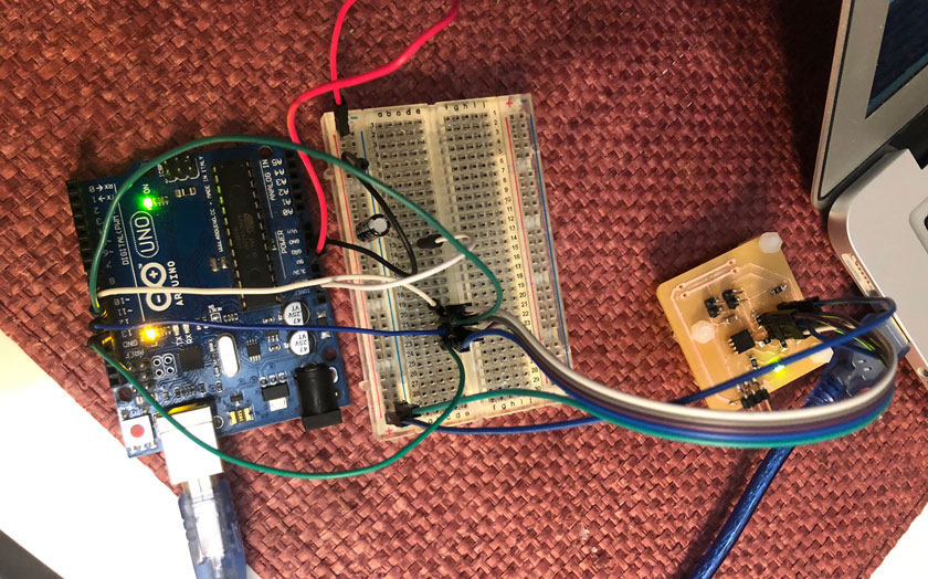
"I2C Leonardo + 3X Arduino Pro mini"
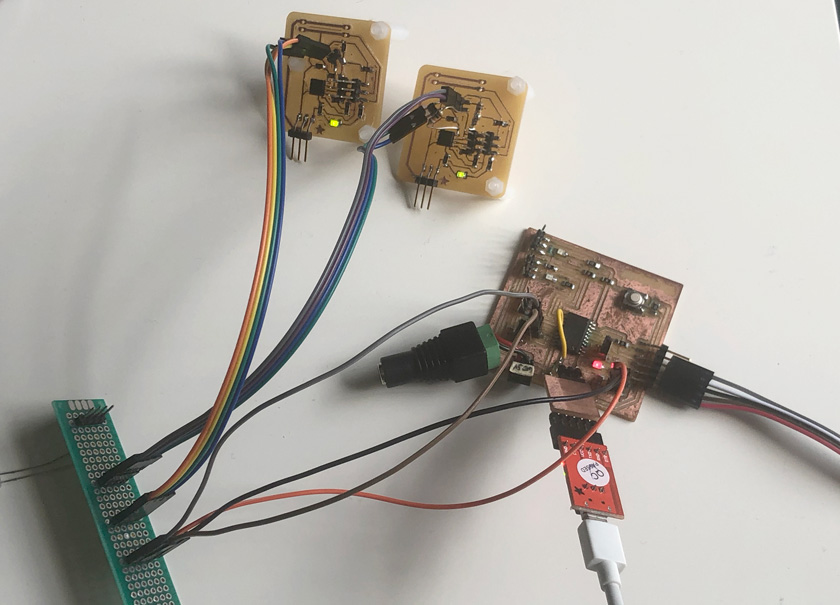
FINALLY WORKING WITH MY I2C NODES!
"I2C Leonardo + 2X Attiny 45 nodes + 1X Arduino Pro mini"
AAAAAAAAAND MY MAIN BOARD & MY NODES ALL TOGETHER YAAAAY!!
This process have been very tough and demotivating as I still don’t know what made the other code not work. However by starting from scratch I have a cleaner and working code.
"I2C Attiny3216 + 2X Attiny 45 secondary nodes"
THE MORE THE MERRIER
As I have only milled 2 Attiny45 nodes and I wanted to try with more, I added one of the Arduino Pro mini aaaaaand it stil wooorks!.
" I2C Attiny3216 + 2x Attiny45 secondary nodes + 1X Arduino Pro mini"
HERO SHOTS
My hero shot for the Networking week is this oen with no doubt. These boards are yet to be improved but for the first time they work as small system that brings me closer to my final project goal.
"Hero shot showing Attiny 3216 main board + two Attiny45 secondary nodes communicating through I2C."
"I2C Hero shot | Attiny3216 + 2x Attiny45"
NEW MAIN BOARD! WELCOME
"Hero shot showing Attiny 3216 main board + two Attiny45 secondary nodes communicating through I2C."
"I2C Hero shot | Attiny3216 + 2x Attiny45 + 1x Pro mini"