4. Electronics Production
This week I manufactured my own in-circuit Programmer to use whenever programming a milled board in the future, manufactured a simple LED blinking board to test this programmer, and also worked with our group to characterize the design rules for the PCB production process on our labs Bantam PCB Mill. (Feb 17)
18-23 minutes
Blinky Test Board
Milling Blinky Board
This week’s assignments of electronic production all revolved around a new machine to me, the PCB Mill. Although there are many different ways of going about creating a PCB, our method of choice was PCB milling due to its cheap material cost, fast turnaround time, and lack of harmful waste products. The process involves using a CNC machine to mill a copper-plated board, leaving traces that can be solder to after milling. Our lab has access to four Bantam PCB Mill, formerly know as OtherMill before a name change. These machines are great, but the software is where the product shines. To control the machine, and send designs to be milled, our lab uses the included Bantam Tools Desktop Milling Machine Software. Our first learning experience of this week was in this software, two of our instructors, Mr. Tom Dubick and Dr. David Taylor covered the interface and workflow for the milling machines.
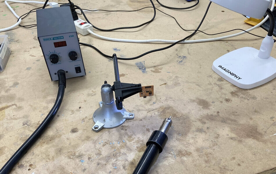
My first project on the PCB mill was a little Blinky Board designed by one of my instructors, Dr. Adam Harris. This board is meant not only to be an intro to PCB milling and electronics production but also to serve as a board to test out the in-circuit Programmer board I make later this week.
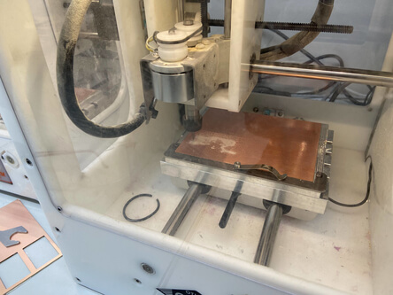
I imported this blinky board file created by Dr. Harris into the Bantam Tools Desktop Milling Machine Software on a computer attached to one of our PCB mills, and began the setup process of the mill before cutting. First I attached my stock material to the bed of the mill. I used a single-sided copper board as my stock and stuck it down to the be with double-sided tape, as clamping materials will cause slights bows in the center, thus leading to imprecise cuts.
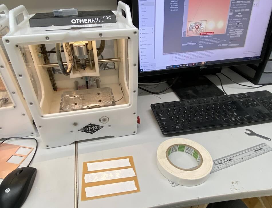
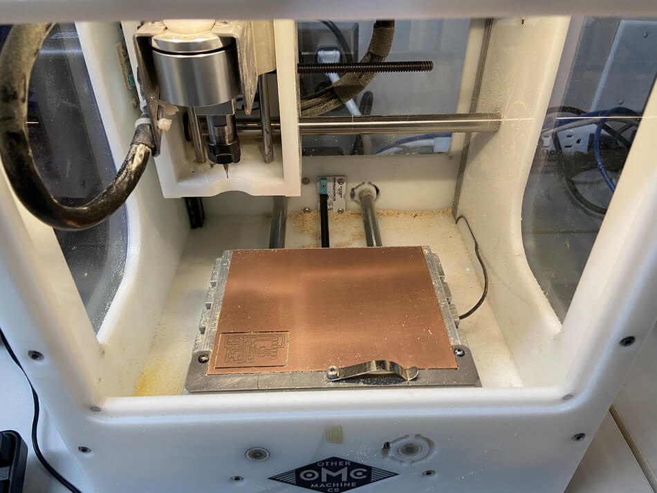
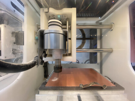
Nextly, I used the change tool feature in the Bantam software, which jogs the gantry of the machine to the center of the machine, and then pops up a selection box to put in your desired tool in the interface. I chose a 1/64” flat endmill bit to cut the traces on my blinky board and installed this bit on the mill before clicking ok on the screen. One of the most convenient features of the Bantam Tools Desktop Milling Machine Software is its ability to find the position of the tool as well as the thickness of the stock material all by itself. I ran these two operations in the interface, and once complete, I had a home machine with set offsets for my stock material, ready to mill. Finally, before milling, I turned off the holes and outline operations, leaving only the trace as that’s the only operation I wanted to cut with the installed 1/64” bit. Below is a video of the entire cut of the traces on my Blinky Board.
Like said in a prior paragraph, the turnaround time from design to physical object when working with small batches is relatively high when milling PCBs, because of the relatively high speeds PCBs can be milled at. The traces on my blinky board only took a little over 2 minutes to cut, and after completion, I followed the same steps I used to install the 1/64” bit used in the first cut, to install a new 1/32” flat endmill bit into the machine. I used this bit for the outline cut of the board, an operation that only took half a minute to finish.
Soldering Blinky Board
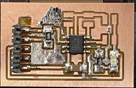
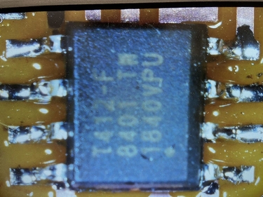
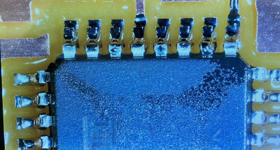
The next step in the manufacturing of a custom circuit board is the ‘stuffing’ of the board or the process of soldering all components to the board. The blinky board I worked on utilized entirely surface mount components, meaning all components were mounted to one side of the board. During our Student Bootcamp week, we completed a Sashakit board as an intro to surface mount soldering. The soldering on the blinky board was relatively simple as it has only an 8 pin chip on it as well as a couple of other small components, however, the board did come with a learning curve. I learned that when milling your own boards from copper, although you remove copper around the traces, copper still remains on the top surface of your board, and with just a little too much solder on one component, this excess copper can become a reflecting pool. Although this mistake isn’t fatal as long as it does not cause any bridges, it doesn’t look as good as the original copper top, and after making this mistake soldering this board I’ve started to learn the balance between too much and too little solder.
Blinky Board Testing
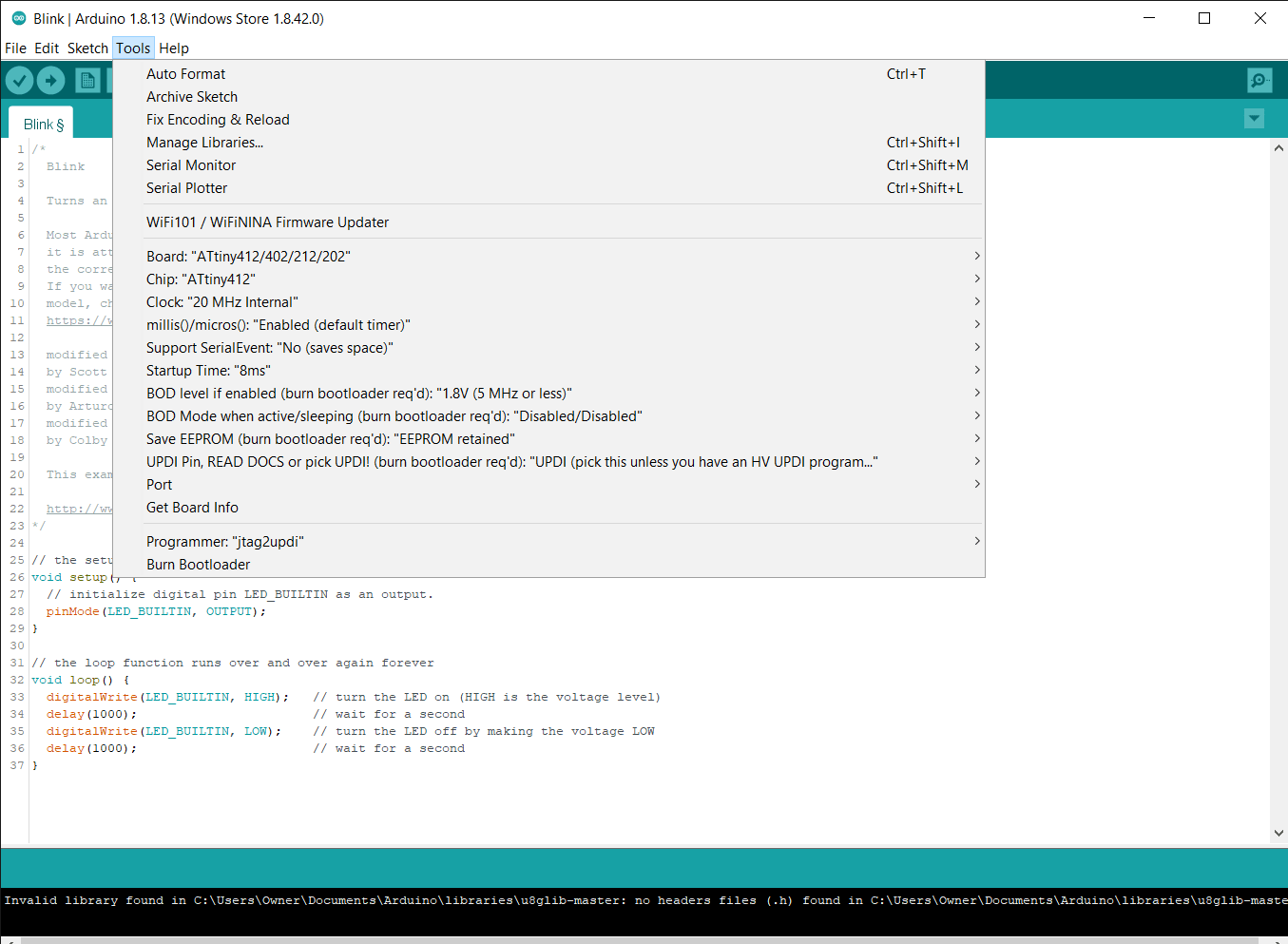
Although we manufactured this board to test out the in-circuit programmer, before serving this function, we wanted to be sure that these boards worked properly and tested the boards by flashing the Arduino Blink example sketch to them to prove the boards working. After a nice explanation from Vincent Zhou, a Fab Academy grad, during my attempts to upload code to my Sashakit discussed on my Student Bootcamp page, I knew the gist of how to upload code via a programmer through the Arduino IDE. Following the same steps I used to program my Sashakit, I attempted to upload the Blink example to the little blinky board using an Arduino Uno clone as the programmer, but my efforts were to no avail. This seemingly simple process of getting this board to blink was actually a process involving hours of troubleshooting. Luckily in my case, the hardware aspects of my board were fine, and I never had to worry about re-soldering any components, or re-milling aboard, despite the little reflecting pool of excess solder I had in the middle of my board. My issues in this process originally stemmed from the lack of any programmer sketch on my Arduino Uno, a step I had forgotten from Vincents workflow. I compiled and uploaded this jtag2updi sketch on the Arduino Uno to complete this step, and then tried uploading the blink sketch to my blinky board via UPDI again. Unfortunately, every attempt I made at uploading this code would upload until the progress bar hit 99%, and then the IDE would send an error message saying,
avrdude: jtagmkII_getsync(): sign-on command: status -1
This error seemed to be universal among the rest of my classmates, as no one seemed to be able to upload the Blink example to the blinky board successfully. After troubleshooting the message for a while, Dr. Adam Harris, one of our instructors, had us hook up the UPDI output pin to a led to see if there was even any signal going to our boards upon an upload attempt. Each one of us tried this test, and none of us even got a flash from the led. From here I knew that the issue was to do with the programmer software itself, as without the led flashing, there was no communication between the Arduino Uno and my blinky board. To start troubleshooting this, I started back from the beginning, and upload the blink skets to the Arduino itself to be sure the board was working. This sketch uploaded and ran successfully, so I moved on to re-downloading and reuploading the jtag2updi code to the Arduino. It was here that I realized that upon downloading and opening this file, the code was being moved into a separate folder inside the master folder, and did not have access to the files needed to successfully upload the programmer code to the Arduino. To address this issue, I moved the code file from the generated folder back into the original downloaded folder and then renamed this folder from jtag2udpi-master to just jtag2udpi, the name of the generated folder where the code was moved. Then I restarted my Arduino IDE and reopened this code, this time being sure it stayed inside the correct folder. I uploaded this code to the Arduino Uno and then attempted the led test recommended by Dr. Harris again. This time to my relief, the led was very dimly lit well connected to the 6th digital pin of the Arduino and after clicking the upload button in the IDE, the led pulsed very quickly. Because of that test, I could be sure that the Arduino was now going to communicate with my blinky board, and I rewired the Arduino to the blinky board by attaching 5v to 5v, GND to GND, and UPDIR on the blinky board to Digital 6 on the Arduino, then oped back up the Blink example in my IDE and re-uploaded via the upload using programmer feature in the sketch menu of the IDE. This attempt gave me a successful outcome, and the IDE finished the upload without any errors, but annoyingly, my blinky board still wasn’t flashing. At this point, I was concerned with the hardware of my board, and the possibility of my led being reversed, but in one last software attempt Dr. Harris had me switch my led pin in the Blink code from output pin 5, which he has specified earlier, to pin 0. I reuploaded this edited code (shown below) to my Blinky Board, and as shown in the video below, it finally flashed.
// the setup function runs once when you press reset or power the board
void setup() {
  // initialize digital pin LED_BUILTIN as an output.
  pinMode(0, OUTPUT);
}

// the loop function runs over and over again forever
void loop() {
  digitalWrite(0, HIGH);   // turn the LED on (HIGH is the voltage level)
  delay(500);                       // wait for a second
  digitalWrite(0, LOW);    // turn the LED off by making the voltage LOW
  delay(500);                       // wait for a second
}
In-Circuit Programmer
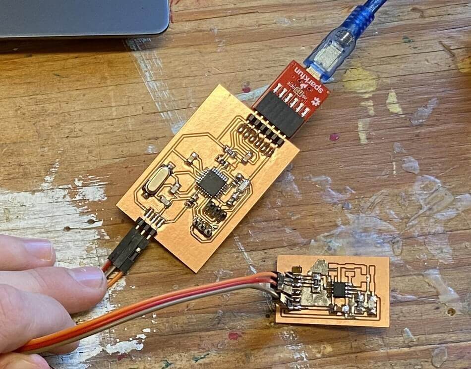
Board Manufacturing
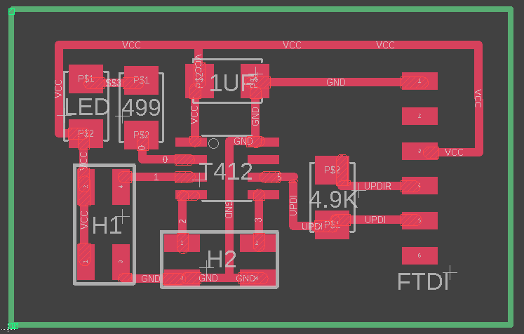
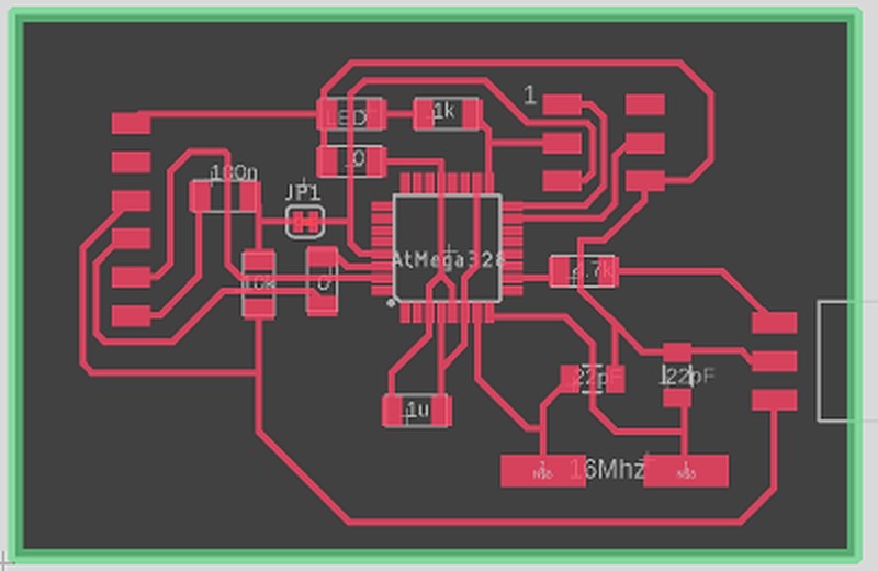
After starting to learn the PCB manufacturing process by making the blinky board talked about above, I spent the second half of the week manufacturing, programming, and troubleshooting my in-circuit programmer. The board I made was designed by Dr. Adam Harris, and uses UDPI to program boards, lowering the number of needed jumpers from 6 (the number needed for ISP communication) to three, one power, one ground, and one data. The board is loosely based on the Sashakit, a board we made in our Fab Academy Student Bootcamp. The programmer uses an ATMega 328, and because of that could be classified as an Arduino Uno, an ability I took advantage of while programming the board. Below is a circuit diagram of this programmer board designed by Dr. Harris.
To mill this board, I followed the same process I took to mill the blinky board. I started by importing the in-circuit programmer board file into the Bantam Tools Desktop Milling Machine Software and positioned the file in the bottom left corner of the workspace. Next, I installed an engraving v-bit on the tool to mill my board’s traces and used the machine’s built-in locating feature to locate the bit. After this, I used the softwares Bit Breaker function to probe the thickness of my material, and I was ready to cut my board’s traces. During this cut, I ran into my first problem with the milling machine itself, a broken band. The spindle on the gantry of the machine uses two rubber bands to spin the tool, and because of the constant stress on these bands, they may sometimes snap. Lucky enough for me, during my cut, only one of my bands snapped, and even with one band gone, the machine can still operate and finished milling my board’s traces. My classmate, Charles DeMey ended up replacing the bands on this machine before milling his in-circuit programmer board.
This board was a little more time-consuming to solder than the prior blinky board due to the larger chip and addition components, but after learning from my first board, I had no huge pools of solder on my programmer board. Unfortunately, this first board I milled and soldered had a faulty chip that gave no output out of any pins. Found this out after finishing the soldering of my board and moving onto board testing. After troubleshooting an error message I received after attempting to upload the Blink example sketch to the programmer board, I took a multimeter to the board itself and found that even when attached to a sufficient power supply, the chip gave not output from any pins. After making this discovery, I had to replace the broken ATMega 328 chip on my board with a working one. I used a reflow station to heat the pads holding the chip to my board, while using a clamp to angle the board upsidedown, making use of gravity to pull the faulty chip down after melting the solder holding it to the board.
Although this process removed the faulty chip from my board, it unfortunately also melted some traces with it, as I gave the reflow a little too much heat. After this mess up, I followed the same steps talked about above and remilled another in-circuit programmer board. While milling this board, I experimented by increasing the Trace Clearance value on traces operation, removing some unwanted copper, and making the soldering process a bit easier. On my original milling operation, I used an engraving v-bit with a .25mm trace clearance, while on my second I used the same bit with a .45mm trace clearance. I found this clearance value to remove enough excess copper to make the soldering easier, while still leaving solid traces. I also found that using an engraving vbit to mill traces on this board left a really clean look on the board, opposed to the 1/64” bit that I used while milling my blinky board, which had a little bit of a rougher look to the traces. I do believe the engraving bit along with the changed Trace Clearance affected my second board, making it even easier to have clean-looking soldering joints, and I’ll definitely continue to use these techniques in the future.
Board Testing
Once manufactured, my programmer board needed to be programmed. Before proceeding with the actual uploading of the boot loader and programmer code to the board, I first did some tests to make sure there were no hardware issues, so I could be sure that any troubleshooting that would have needed to be done was solely on the software side. After my failed first board, I started off by powering the board with 5v through an Arduino Uno and using a multimeter to see if I was getting a voltage from the pins of the chip. Lucky for me] my second chip seemed to be working, so next, I moved on to testing the board itself. I hooked up my programmer board to an Arduino Uno with the ArduinoISP sketch flashed on it, connecting the ISP pins on my programmer to 5v, ground, and digital pins 10-13, as shown in the diagram below.
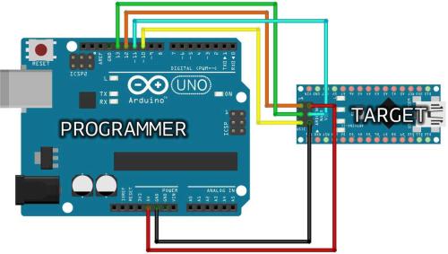
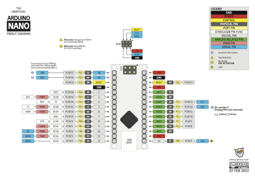
Although this diagram pictures an Arduino Nano, I was able to use an image of the pinout of the Arduino Nano along with the circuit diagram of my programmer to align the pins properly.
Programming
After connecting the programmer to the Arduino Uno via ISP, I was able to use the Arduino IDE Upload Using Programmer feature to upload the blink sketch to my programmer board. Although the code uploaded to the board successfully, the led on my programmer didn’t blink because I had the wrong led pin set in the Blink example sketch. After a bit of looking I found that although labeled as pin 17 on my AtMega 382 chip, the pin I was using to control my Arduino was referred to as pin 13 by the IDE. This is because on the Arduino Uno itself, pin 13 controls the led, and because I used the Arduino Uno board profile to upload code to my programmer, I had to take this into account. After changing this pin from 17 to 13 in my sketch, and reuploading it to my programmer, my led flashed and I could confirm my programmer had no hardware issues. Nextly I moved onto flashing the actual programmer to my programmer board. I left my board connected to the Arduino via ISP, and used the Arduino IDE Burn Bootloader feature to flash the Arduino bootloader to my chip. Next, I compiled the same jtag2updi code file I used to upload code to my blink board, and uploaded this to my programmer. All the troubleshooting on this jtag2updi file on my previous blinky board work came in hand here, and I was able to upload the same file to my programmer board through and Arduino Unos IDE. I tested that this upload was successful by attaching my programmer board to power and attaching an led to the UPDI pin of the board. This led was dimly lit, proving that the code uploaded properly, and the UPDI pin has no shorts and can communicate as an output. Our board design has a small feature in the reset trace allowing the trace to be cut once the programmer has been programmed, so after this successful test, I cut the trace with an Exacto blade. This trace is cut to prevent the programmer from ever being reset, as once the jtag2updi sketch has been uploaded, I want to keep that file on my programmer board, and without this trace being cut, any code I try to put on a chip through my programmer would just replace the jtag2udpi sketch on my programmer itself, and not upload to the desired chip. I then moved on to testing my programmer itself. I used the blinky board I manufactured earlier in the week and wanted to upload the same Blink example sketch but instead of using an Arduino Uno, I used my in-circuit programmer board. Before attempting this, I first reset the code of the blinky board, as the blink sketch I had uploaded with the Arduino to test the board was still on it, and I wanted to be sure my programmer could send the code to the board. After this, I attached my blinky board to my programmer with a 5v, ground, and data (UDPI) pin, and also my programmer to my computer with an FDTI chip. This FDTI chip attaches to the 6 headers on the side of my board, facing upsidedown, a bit that I found out after troubleshooting why my board wasn’t powering up for a while.
Once the programmer was connected to my computer, I changed my board type to the 412 chip, the chip used on the blinky board, and also changed the programmer to jtag2udpi so the IDE could communicate with my programmer. Then I used the Upload Using Programmer feature of the IDE to upload the blink sketch to my blinky board via my programmer and, as shown in the video below, I was able to successfully upload this code to my blinky board.
Summary
Being my first time following the PCB production process, I learned a lot this week, from milling machine prep, all the way to new techniques for my surface mount soldering. I enjoyed the process of using the PCB mills, and feel more comfortable with the process after this week. In addition to that, I believe I gained some more skill when it comes to surface mount soldering of copper-coated boards, as although my first blinky board of the week had some little reflecting pools, I was able to better control the amount so solder used on my in-circuit programmer, a practice that I will keep in mind while continuing the course.
Group Work
In addition to this week’s personal assignments, we had another group assignment. The assignment was to characterize the design rules for the PCB production process on our labs Bantam PCB Mill We documented this whole process on our Fab Academy group page with a little help from some of my classmates. In this week’s group assignment, I worked with my classmate, Graham Smith, to generate the test files, complete the machine testing, and document our steps taken, and results found on our group site. Click here to view our group documentation site, with this week’s assignment on it.
Downloads
- Click Here to access and download all of my files from this week