6. Electronics Design
This week I learned the steps before PCB milling, using Autodesk EAGLE to create my PCB schematic and millable board file, and then manufactured and tested this board. (Mar 3)
21-27 minutes
Button Blinky Board
Eagle CAD Setup
To complete this week’s Electronics design assignment, I used Autodesk EAGLE to create a schematic and board file for a little board containing an ATTiny 412 chip as well as an LED and a Button. Although I was not experienced with EAGLE, I had a little prior knowledge of the interface due to some work we did in our Electrical Engineering class. I worked through Part 1 and Part 2 of the Autodesk EAGLE Live: Getting Started with EAGLE video series for an assignment in this Electrical Engineering class, and I found it helpful to look back on these intro videos while refamiliarising myself with the EAGLE workspace this week.
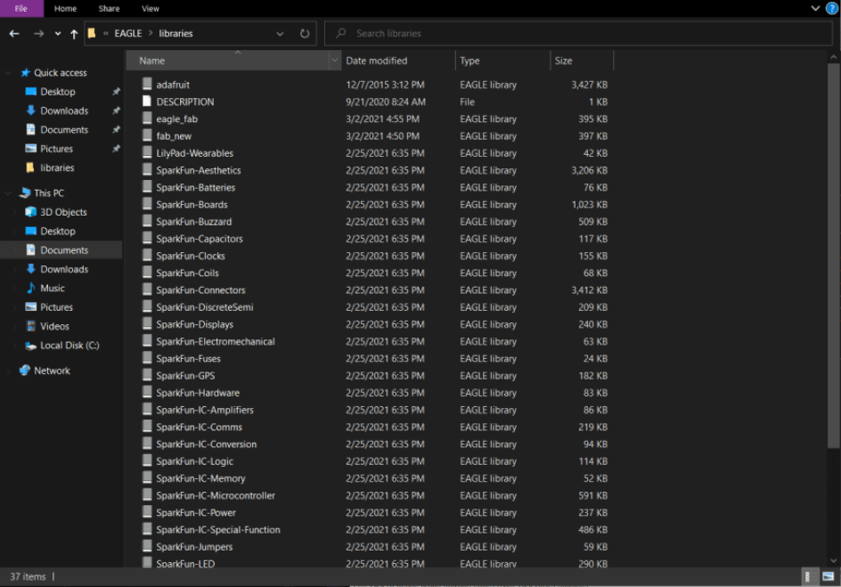
Before starting any design work in EAGLE, I had to set up some parts on the interface to work with the parts and tools accessible to me. I started by installing the Fab EAGLE Libary, a library containing EAGLE footprints for parts we have access in our lab, as well as the Adafruit and SparkFun libraries, which had some additional needed parts. After downloading all of these libraries, I unzipped all of my downloaded folders and moved all of the .lbr files contained into the EAGLE libraries folder, found under the softwares files system on my computer.
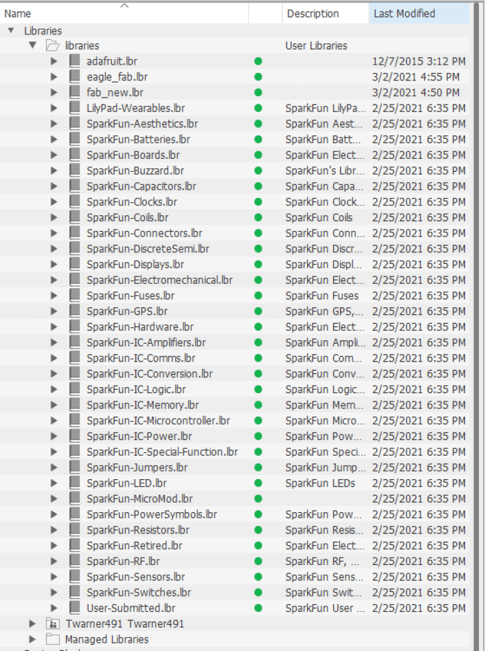
Upon importing all of these new libraries, EAGLE updated its interface to include these new files under the folder in the interface. Before moving on, I was sure to select all of these folders and click use, confirming this action by being sure the dot next to the library name was green.
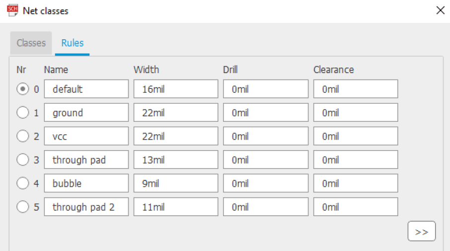
With all these libraries installed in EAGLE, I moved on starting a new schematic of this button blink board I designed. Before starting on the schematic itself, I edited the designs Net Class Rules by going to the Edit tab and selecting Net Classes, whitch pulls up a pop up winodw allowing me to set parametric rules for different net-type I setup.
Eagle CAD Design
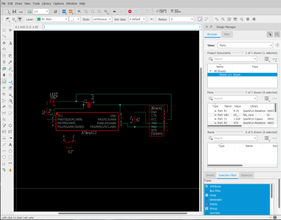
Once all of this setup work was completed, I moved onto creating my first board of the week. The board I designed is based on the little Blinky Board designed by one of my instructors, Dr. Adam Harris, that we made in our week 4 assignment. This blinky board uses an ATTiny 412 chip to blink a small LED on the board and features an FTDI header to connect to a programmer.
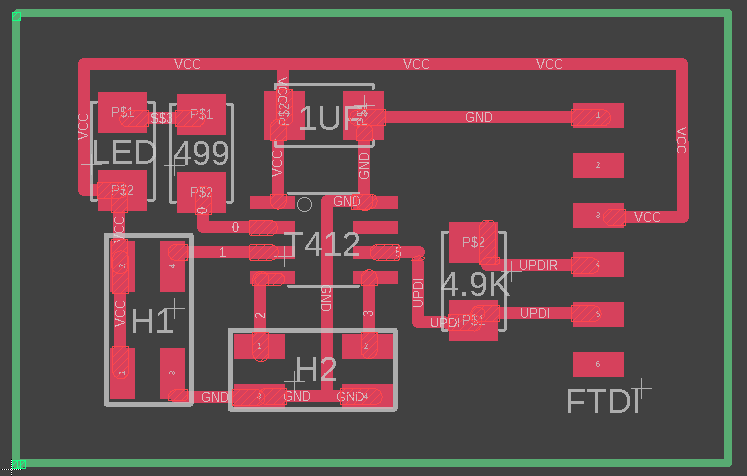
Using this Blinky Board diagram as a reference, I created my schematic in EAGLE featuring an ATTiny 412 and some FTDI headers just like the Blinky Board. I first started by adding in all the components needed on this blinky board from the library I had installed previously. I added each of these components by first locating the correct part in one of the libraries, and then clicking to add the part to my schematic itself. This board only required seven components, making this process pretty pain-free, and with all of them added, I moved on to set values on these components. On the parts in my schematic that required a value, I used EAGLE’s Info tool to open up an options menu for each part, and typed out the correct value for each component. Finally, I used EAGLE’s Wire tool to connect all of these separate components and complete my Button Blinky Board’s schematic.
With this schematic for my Button Blinky board finalized, I moved on to generating a board file from my schematic, so I could then work on the board’s layout. I generated this board file directly from my schematic, by clicking the Switch to Board button in EAGLE, and then by clicking Yes when prompted to generate a board from the schematic.
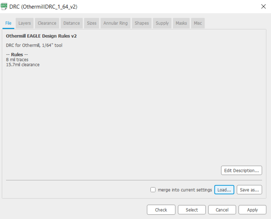
Before doing any work with this new file, however, I had to set design rules for the file corresponding with the machine and bits I would be used to mill the board. I used one of our labs Bantam PCB Mills along with a 1/64” Endmill bit to mill the traces on my board, and therefore had to take these into account when setting design rules for my board design. I followed this guide by Bantam Tools themselves while setting up these design rules, making use of a preset design rule found in that article, the DRC for Othermill, 1/64” tool, and loading these design rules into the design rules tab in EAGLE with the Load button. This preset defined Layer, Clearance, Distance, Size, Annular Ring, Shape, Supply, and other miscellaneous settings in my EAGLE board file.
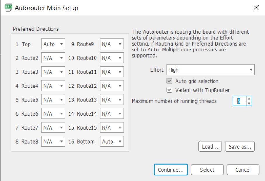
With these design rules set, I was finally ready to tackle the process of board layout for my Button Blinky board. I first used the Move tool in EAGLE to orientate all of the board’s components in the board’s workplace. Next, I moved onto the routing of traces on my board. Autodesk EAGLE is equipped with a powerful Autorouting tool that I took advantage of during this process. Although this tool is incredibly powerful, It still cannot match human trace routing but was plenty sufficient for this small Blinky Board. After clicking to run the Autorouter tool, I filled out all settings, leaving Top and Bottom layers on the Auto, and all others on N/A, and also set the effort to the High setting, addressing 5 threads to run the operation, before clicking continue to run the auto-routing script generated.
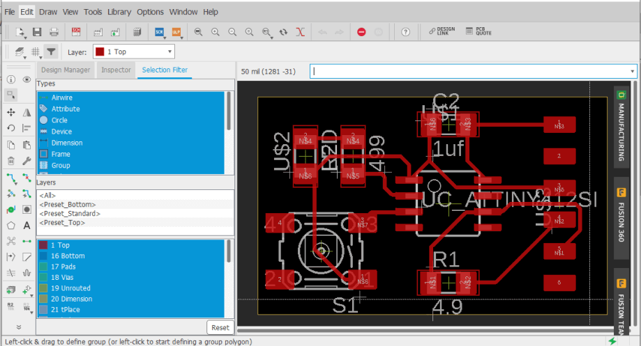
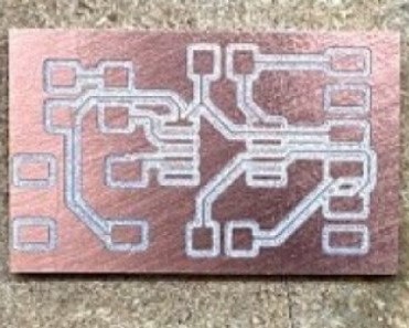
Because of the simplicity of this board, the autorouter didn’t take much time at all to complete and converted the rat’s nest generated by my boards schematic, into a nice-looking board with well-run traces. Before I could call my board finished, however, I had to set the size of the board’s outline. I did this by selecting layer 20 of my design, the Dimensions layer, and then dragging the yellow rectangle using the Move tool to surround the board’s components tightly.
Milling
Once my design work for this blinky board was complete, I could move onto the board’s manufacturing process, starting with milling the boards itself. I followed the same steps I used to produce my boards in week 4’s electronics production class to manufacture this board. I first save my EAGLE board design as a .brd file and moved that file onto a computer attached to one of our labs PCB mills. Here I was able to import the .brd file into the Bantam Tools Desktop Milling Machine Software, and set up the settings for this milling job. I used the softwares Tool Change function to jog the gantry to the center of the machine for easy bit access where I installed a 0.005 PCB engraving bit onto the spindle, and then select the preset tool profile for the newly attached tool in the softwares popup window. After this, I used some double-sided tape to attach my stock material to the bed of the machine, in this case, a single-sided copper PCB blank. With this new tool attached and the stock material in place, I located the tool and my stock material with the softwares Bit Breaker function, selected the Traces feature to be cut, and set a trace clearance of .035mm under the advanced tab in the GUI. I found in my testing in week 4 that a trace clearance between 0.3mm and 0.5mm leaves optimal trace width to prevent tears, while still leaving ease in the soldering process.
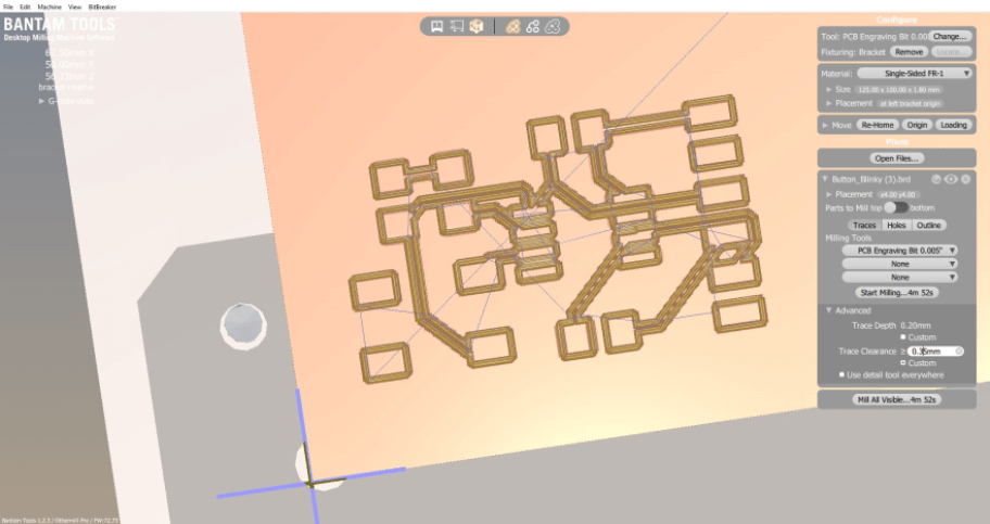
The milling of the board’s traces was successful on the first attempt, so after its completion, I changed the tool to a 1/32” bit and then followed the same setup steps take above to mill the board’s outline. In my Eagle design, I had set a rectangular board outline under the Dimensions layer in my board file, allowing me to run the same board file I used for milling traces, by just disabling the Traces feature and enabling the Outline feature under the files settings on the right side of the screen in the Bantam Tools Desktop Milling Machine Software. I ran the selected Outline feature on the milling machine, and successfully cutout the rectangular board shape around my traces.
Soldering
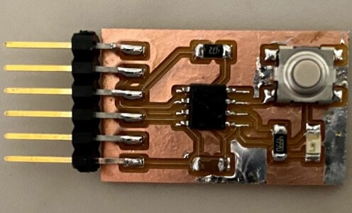
Due to the simple nature, and low part count of this board, the “Stuffing” process of the board went by with no major pains. After the milling operation of the board was completed, I washed off the board with soap and water to remove any excess grease/debris on the copper, dried it, and moved on with the soldering process. Like all other boards I soldered before this one, I followed the process of working from the inside out, starting in the middle by soldering the ATTiny 412 chip to the board, and working my way out, soldering the resistors, capacitor, and an LED, before moving onto the taller button and pin headers. Unfortunately, on a couple of these components, I had a little too much solder on my iron and left some little solder pools on the copper surface of the board. I’ve found throughout all of the surface mount soldering I’ve done in the class so far that using solder flux while soldering allows me to get clean and aligned solder joints. I like to use a syringe of flux with a fine end tip to apply flux to the board’s pads, before sticking down a surface mount component. I used this flux method for each of the 6 components on my boards, as well as for the board headers.
Testing
Despite these little solder pools, I had no hardware issues with this board, and after soldering, the board was recognizable through my laptop and programmer, and therefore I was ready to test my board through programming. This process was where most of my troubleshooting this week took place, due to an error in my original board schematic. While designing my Button Blinky Board, I planned on taking advantage of an internal pull-up resistor inside the ATTiny 412 chip to use with my board’s button. Before designing the board around this practice, I found the datasheet of the chip and confirmed the presence of a pull-up resistor on the chips pin 1, the pin my button would be attached to. When first attempting to program my board, I edited the generic Arduino IDE Blink example for my boards LED, and also added a couple of lines of code setting up my board’s button as an input with a pull-up resistor, and an if statement turning on the LED when the board’s button was pressed. That code looked like this
// the setup function runs once when you press reset or power the board
void setup() {
  // initialize digital pin LED_BUILTIN as an output.
  pinMode(0, OUTPUT);
  pinMode(1, INPUT);
  digitalWrite(1, HIGH);

  }

// the loop function runs over and over again forever
void loop() {
if(digitalRead(1)==0){
  digitalWrite(0, HIGH);   // turn the LED on (HIGH is the voltage level)
  }
else{
  digitalWrite(0,LOW);
  }
 }
}
with the line
pinMode(0, OUTPUT);
setting up my boards LED as an output attached to pin zero, and the two lines
  pinMode(1, INPUT);
  digitalWrite(1, HIGH);
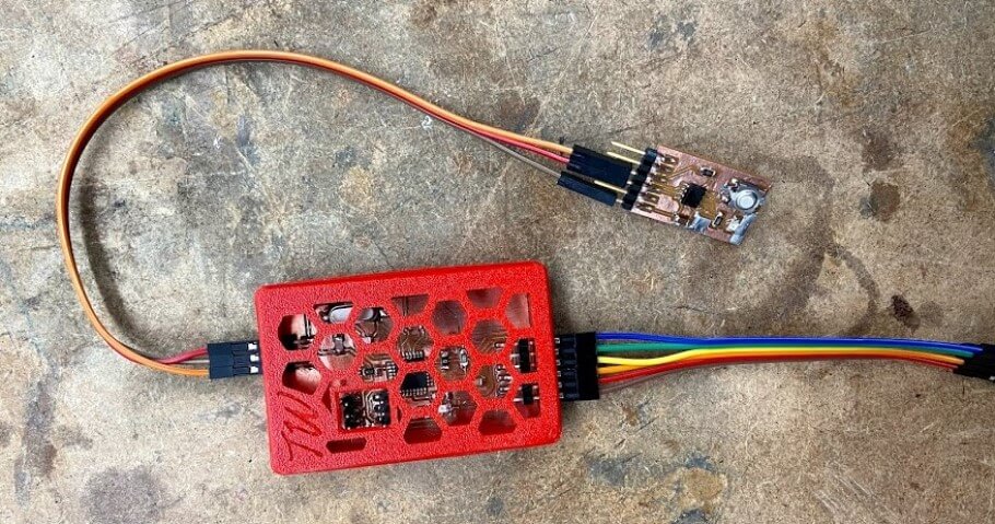
addressing pin 1 as my board’s button input pin, and activating the ATTiny 412 chips internal pull-up resistor. The process of turning on such resistor involved writing a high value to digital pin one. Due to the addressing of this pin as an input, the theory of this code is that the 412 chip will be confused by this request, and infer that that high value should run to the pin’s pull-up resistor, thus turning it on. With this code flushed out, I attached my newly made button blinky board to my UPDI in-circuit programmer I worked on in week 4’s electronics production class and then connected my programmer to my laptop through the programmers FTDI headers.
I uploaded this code from the Arduino IDE through my in-circuit programmer board to my button blinky board using the IDE’s Upload Using Programmer feature. Luckily enough, this upload worked the first time, however upon uploading the code, the LED on my board remained on at all times no matter the state of the button, unlike the intention of my code to turn the LED on when the board’s button was pressed. Originally my fear was a short somewhere on the board, connecting the button terminals. However, after some investigation under a microscope and with a multimeter testing continuity, I found no hardware issues anywhere on the board and moved onto software troubleshooting. My next guess at an error was the possibility I had addressed the boards button to the wrong pin on the ATTiny 412, but after a look back at my schematic, I found this to not be the case. I was stumped here and called on the help of one of my instructors, Dr. Adam Harris, who had me experiment to be sure the pull-up resistor connected to the button pin was activated. While doing this, I rewrote the two lines addressing the button and turning on the pull-up resistor to
  pinMode(1, OUTPUT);
  digitalWrite(1, LOW);
to measure the output pin connected to the button with a multimeter to check any resistance. Weirdly enough, however, after changing these two lines, and reuploading this code (attached below) through the programmer, my button blinky board worked as intended, turning the board’s LED on and off in correspondence with the state of the board’s button.
// the setup function runs once when you press reset or power the board
void setup() {
  // initialize digital pin LED_BUILTIN as an output.
  pinMode(0, OUTPUT);
  pinMode(1, OUTPUT);
  digitalWrite(1, LOW);

  }

// the loop function runs over and over again forever
void loop() {
if(digitalRead(1)==0){
  digitalWrite(0, HIGH);   // turn the LED on (HIGH is the voltage level)
  }
else{
  digitalWrite(0,LOW);
  }
 }
}
This success confused me due to the lack of engaging the chips pull-up resistor at all, and also the fact that I had set the button, an input component, as an output. I probed the entire board again using a multimeter in hopes of finding an answer for this success but this was to no avail. It wasn’t until I looked back through my original circuit schematic with Dr. Harris that we realized that the button on my board was attached to the VCC line over the board’s Ground. The circuit was making use of the internal resistance of the 412 chip in combination with the button being set as an output to receive button data, and flash the light. Although this attachment of the button to VCC was a flaw in my original board schematic design, the error could be worked around through software, and my blinky button board worked as intended, turning the boards LED on and off in correspondence with the state of the board’s button, as shown in the video below.
Summary
Being my first time completing the entirety of the PCB production process, from board design to board stuffing and testing, I learned a lot this week. I found it super helpful to begin my Eagle work for my button blinky board along with the rest of my group mates and one of our instructors, Adam Harris, as we could bounce ideas and best practices off each other. I began to pick up the Eagle interface over the course of this week, and after the completion of this week’s assignment, began some more work in the interface on a final project board, documented below. Overall this week, I became much more comfortable with using Eagle and also bettered my surface mount soldering skills, finding my liking of flux, and figuring out the right amount of solder.
Group Work
This week’s group assignment was to use our lab’s test equipment in your lab to observe the operation of a microcontroller circuit board (in minimum, check operating voltage on the board with multimeter or voltmeter and use an oscilloscope to check noise of operating voltage and interpret a data signal). I worked with two of my groupmates, Drew Griggs and Graham Smith, on this week’s tests. Starting, one of my instructors, Tom Dubick, gave us an overview on the functions and usage of an oscilloscope. Using this tool, we probed the PWM signal in a simple Arduino circuit, where a servo is controlled by a potentiometer. We observed the PWM through a difference in voltage across the servos data and ground pins. In addition to this testing, I used a multimeter to probe my blinky board made in the electronics production week of this class, measuring voltage across an LED, while running a blink sketch and also testing the continuity of the diode. Click here to view our group documentation site, with this week’s assignment on it.
Downloads
- Click Here to access and download all of my files from this week
Final Project Board Work
In addition to completing this week’s board design assignment, I also started work on a potential board for my final project.
Design Work
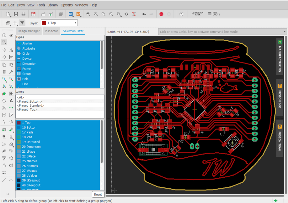
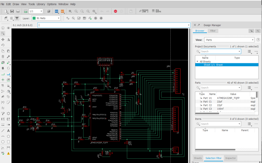
I started this final project board design process following the same steps I used while creating my Button Blinky board and began the process by creating a schematic of my board. Throughout the schematic creating process, I referenced a prior Fab Academy final project, the Sashakit “an Arduino compatible, fabbable board, and also an improved version of Fabkit.” (Quote from the Sashakit I found that looking at the labeled schematics and board designs for the Sashakit give me the information I needed to dive deeper into the workings of a microcontroller. Before starting any work in Autodesk EAGLE, I used the Sashakit schematic to find the parts needed on an Arduino-like board, and the connections of some of these components to the board’s chip. I also took some time to write out my needs on a final project board and was able to use all of this pre-work to start creating my final project board schematic. Unlike my blinky board, instead of starting this schematic by laying out piece by piece the needed components, and then connecting them, I worked system by system, adding components as I went until I had a finished schematic. I found this approach to be more assistive in my understandings of how the components interact with each other and also allowed me to do some additional research on the different needed sections while working on them. I finished all major sections of my schematic following this approach, and the only editing that I had to go in to add later were 0-ohm jumper resistors, a component I used to connect traces at intersections while designing my final project board.
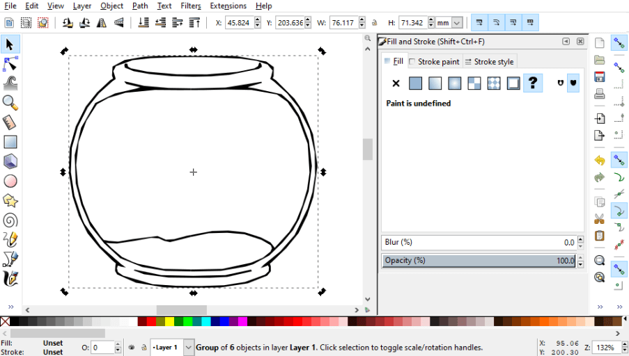
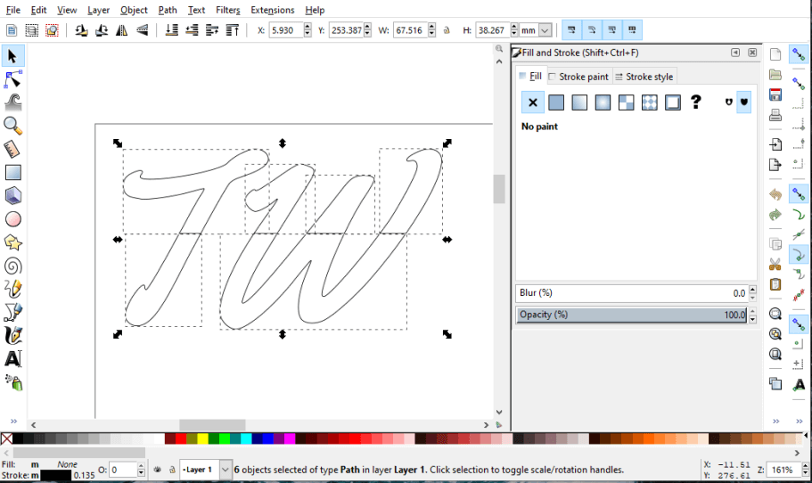
With this schematic done, I moved onto generating my final board file, following the same steps taken while generating this file for my button blinky board. Unlike the generation for the blinky board, however, I wasn’t entirely happy with the default generation for my final project board, as I wanted it to have a little more flair, so I set off to add a custom board shape, and some icons to my board design before routing any traces on the board. After doing some research on this process, I found this good article on Importing Custom Images into Eagle, a process easier said than done. Although this process of importing images and shapes into EAGLE is entirely possible, the software cannot handle the importing of any closed polygons or shapes with complex curves of any kind, and therefore any images/icons you want to be imported require a good bit of prep work. I completed this prep work in Inkscape on my desired board shape, a fishbowl, as well as on a little fish icon, and a TW logo for some more personalization. The prep work process for all these images was the same in Inkscape, starting with tracing the bitmaps into SVGs of these images after opening them in Inkscape. This step was to dive by right-clicking on the imported bitmap and selecting the Trace from Bitmap tool. This process generated a scalable vector graphic of the imported bitmap, that I could then start to alter so it could be imported into EAGLE. My workflow of altering this graphic started by resizing the Inkscape page by going to
File > Document Properties
and the selecting the Resize page to drawing or selection button under the Custom Size window. After this, I converted the graphic into a path by selecting Object to Path under the Path tab and the top of the Inkscape GUI, and ungrouped all parts of this path by selecting everything in the design, right-clicking, and then selecting Ungroup. Nextly, I navigated to
Extensions > Modify Path
Where I used the Add Nodes tool to add excess nodes to my design. Under this same menu, I removed any complex curves that EAGLE would not be able to handle by using the Flatten Beziers tool with a flatness value of 8. Finally, to address EAGLE’s inability to import closed polygons, I used the Division tool under the Path menu to cut any closed polygons in half, and then separated all of these nodes by using the Break Apart tool under the same menu. This process adds some unwanted dividing lines, that can be removed once imported into EAGLE, but these lines allow for the successful importing of these shapes in the first place, so are required.

Once all this pre-work in Inkscape was complete, I saved each of these altered files as a .dxf file to my computer from Inkscape. To import these .dxf files into EAGLE, I found making use of the import-dxf plugin for EAGLE worked the best. After installing this ULP into EAGLE following the instructions provided by the import-dxf Github, I opened my final project generated board file in EAGLE and ran the command
run import-dxf
This line opens the import-dxf interface, where the desired .dxf file can be selected, and then imported into a specific layer of a board design. I imported my fishbowl .dxf into layer 20 of my design, the Dimensions layer, to replace the generic rectangle board profile, and then ran the same command to import both the fish icon, and the TW logo, but to the Top layer over the Dimensions. Because these shapes are on the Top layer of my board design, they will both be milled as traces instead of being included with the outline shape of the board. With all of this importing work done, I had a template to start routing the traces of my board around. Although I made use of EAGLE’s Autorouter tool to complete my button blinky board earlier this week, I opted for the hand routing process for my final project board, as after attempting to autoroute a coupe, times, I just wasn’t happy with the results. This also gave me the ability to utilize parts like 0-ohm resistors as jumpers over weird interceptions of the board, a technique I took advantage of while routing the traces on this board. This hand routing process was relatively tedious and pretty time-consuming, but I think the results look great and work much better than the autorouter generated traces with the weird constraints put in place by the odd board shape.