7. Electronics design
This week the assignment was to redraw an echo hello-world board circuit, adding minimum a button and a LED. It is necessary to check the design of the circuit, make it; and to test if it is working properly. Bellow the circuit and components of the hello-world board that should be updated adding a button and a LED.
Circuit Design - Eeschema
Version 1
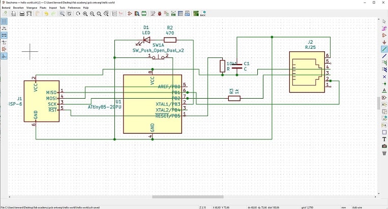
The software used to create the circuit was Kicad. Kicad has a schematic capture software called Eeschema (documentation) that enable to design circuits lines and add components. It provides useful features like ERC (Electrical rules check) that helps to control incorrect or even missing connections in the circuit. I began to draw the circuit adding the basic components: RJ25, ISP-6, Attiny-85, LED, button, capacitor, and resistences.
After placing the components in a good position to provide a good view, I have added the lines of the circuit, connecting the pins of the components in the position to connect them, as seen in the image bellow.
Version 2
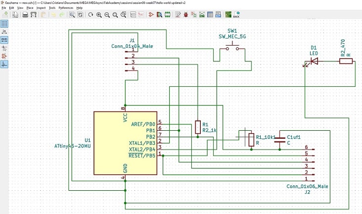
The footprint of the components used in the circuit schema version 1 was different from the real components we have available and would sold in the board. I have updated the footprint of the circuit schema to match the correct components were were using to sold the board. I needed to replace the position of the components in the schema to help the design of the board. Bellow the same circuit using the correct footprint of the components.
Circuit Design - KiCad
Version 1
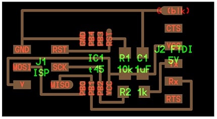
KiCad uses the drawing from Eeschema to generate an interface to place the components in the final board that will be create and the lines. After this step, a file can be generated to send it to the milling machine to mill the board with the circuit. It was not easy to find the best lines for the circuit since KiCad does not provide a easy framework to select the correct components for the board. I took sometime to find a better solution for this and then be able to draw the lines. Then I had to think how to connect the pins of the circuit without having cross lines. Bellow, the resulted board drawing at KiCad.
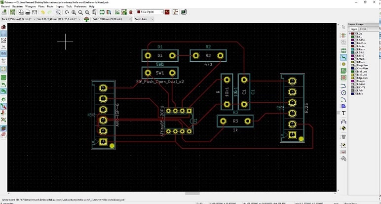
Download the ZIP file containing the KiCad files of the circuit.
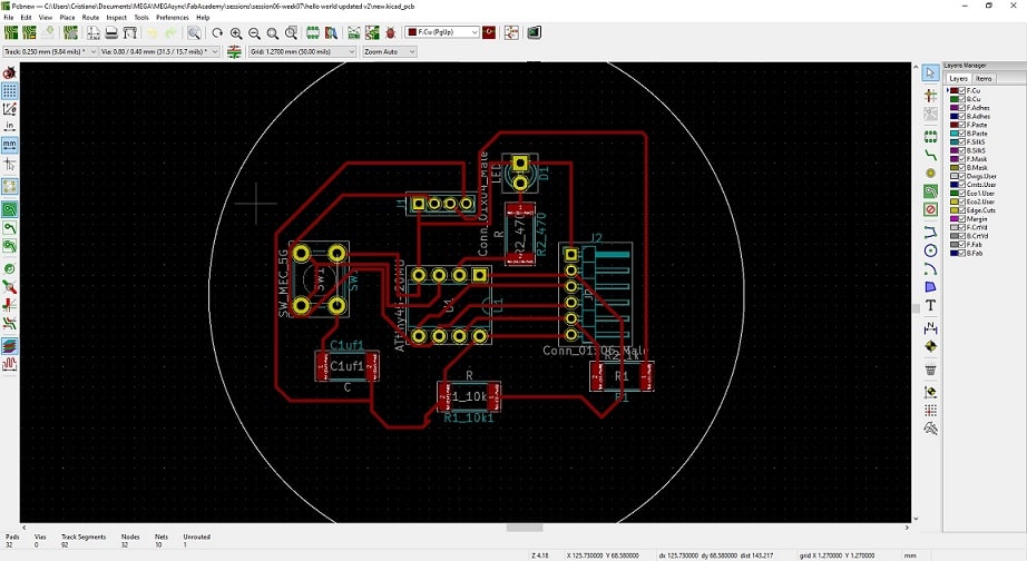
Version 2
Consequently after the changes in the footprint of the circuit schema, the design of the PCB had to change as well. I needed to redraw the lines of the board to match the new schema. Moreover, the size of the board version 1 were quite big and some components could not be solded on it. In this new version, the dimensions of the board were changed to generate a smaller board which would enable to sold the components. I took care for the lines have a good width to avoid problems during the milling process.
Milling board
Version 1
From the drawing board created at KiCad, it was created the files that could be used by the milling machine to mill the board. To create the file use the menu Export next to Printer in the tool bar. In the window open, select the desired layers to export and enable the checkbox “Negative plot”. This flag will create the file that will be used in the milling machine. The important layer to select is the F.Cu, where the components and lines were placed.
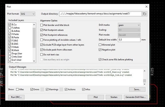
Export window to generate file to milling machine
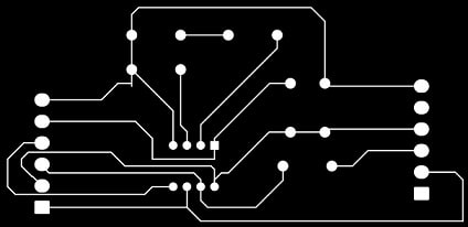
Image used to mill the board (Version 2)
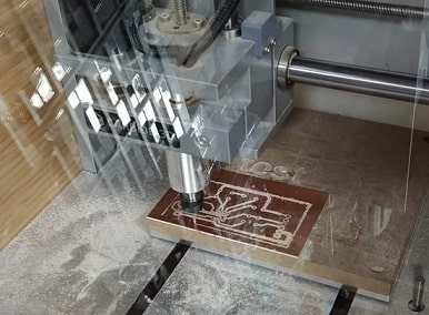
Milling machine creating the board
Before milling the board, make sure the board that will be milled is fixed in the machine.
Otherwise the board can move and you need to restart the milling process from the scratch.
Download the SVG file used to mill the board.
Version 2
Using the same procedure used for the board version 1, it was generated the lines of the board version 2. This is the new lines used to mill the hello world updated board.
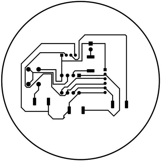
Image used to mill the board (Version 2)
Download the SVG file used to mill the board version 2.
Soldering the components
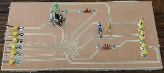
Version 1
For this it will be necessary the following list of components:
- one LED
- three resistences: of 470, 1k, and 10k ohm
- one capacitor of 1µF
- jumper for RJ25 and ISP-6 (12 in total)
- and attiny85.
All components were added to the board, except the attin85 because it is necessary an extensor that we were out of stock in our lab.
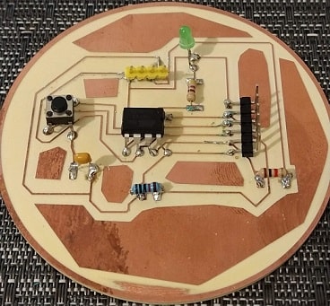
Version 2
The following components were reused to sold the board version 2: (i) LED; (ii) three resistences (470, 1k, and 10k); (iii) capacitor of 1µf. It was used a button with four connections (although they are mirrored). The ATtyne85 was exchanged by ATtiny45. The jumper ISP-6 used was folded ones and the FTDI was normal jumpers (4 pins).
Programming the board
Version 1
Unfortunatelly, it was not possible to program the board since the Programmer was not ready yet because of error during compilation of its source code. This will be done as soon as we can figure out the error in the Programmer.
Version 2
To upload the code in the board, it was used Arduino as interface between the computer and the hello world board version 2. The configuration needed to Arduino works is explained at 5. Electronics production, section Programming board > Setup Arduino. The connection used between the board and the arduino, is also explained in the previous link. Important to use the correct order of the jumper ISP-6 from your board in the arduino, otherwise it will not upload the code. Bellow there is the order of the jumper ISP-6 from top to bottom in the previous image (board version 2).
| J1 - ISP | Attiny | Arduino |
|---|---|---|
| GND | GND | GND |
| RST | PB5 | D10 |
| MOSI | PB0 | D11 |
| MISO | PB1 | D12 |
| SCK | PB2 | D13 |
| V | VCC | V |
The LED is connected in the PB3 connection from the ATtiny45 and the button is connected in the PB4. To program the board we need to use these constants in the code and change/read their values.
The program to be loaded requires to implement two methods: setup and loop. The former one is executed uniquely once when the board is connected to electricity. The second one is executed constantly while the board has electricity. You might use the function delay to be able to notice changes in the LED or button, otherwise some changes will not be noticed because of the speed of processing time. For this assignment, I have tested the following two simple codes.
Simple blink code
This code blink the LED each second. The first thing needed to execute the code is initialize the output LED, done with the function pinMode. Notice the use of the function delay(1000), it receives the time in miliseconds. The variable LED was added to point to the ATtiny pin of the LED. The function digitalWrite changes the state of the pin to HIGH or LOW, respectivelly has electricity or not.
int LED = PB3;

void setup() {
  // initialize digital pin LED_BUILTIN as an output.
  pinMode(LED, OUTPUT);
}

// the loop function runs over and over again forever
void loop() {
  digitalWrite(LED, HIGH);   // turn the LED on (HIGH is the voltage level)
  delay(1000);                       // wait for a second
  digitalWrite(LED, LOW);    // turn the LED off by making the voltage LOW
  delay(1000);                       // wait for a second
}
Button turn LED on
The second code uploaded turn on the LED when the button is pushed. The setup function initialize the push button as INPUT, and the LED as output (using the respective ATtiny pins). By default, the button has a closed circuit, which means that is constantly sending electricity where its connection. When the button is pushed, it opens the circuit, which means it stops to send electricity. The status of the button is gotten using digitalRead function. If the value read is low (meaning the button is pushed), the program turn the LED on (digitalWrite using HIGH value). Otherwise it turns the LED off (LOW value)
int pshbutton = PB4;
int LED = PB3;

void setup() {
  // put your setup code here, to run once:
  pinMode(pshbutton, INPUT_PULLUP);
  pinMode(LED, OUTPUT);
}

void loop() {
  // put your main code here, to run repeatedly:
  if (!digitalRead(pshbutton))
    digitalWrite(LED,HIGH);
  else
    digitalWrite(LED,LOW);
}