7. Electronics design
Assignment
- Group project
- use the test equipment in your lab to observe the operation of a microcontroller circuit board
- individual project
- redraw an echo hello-world board, add (at least) a button and LED (with current-limiting resistor) check the design rules, make it, and test it
- extra credit: simulate its operation
Group Assignment
- Use the test equipment in your lab to observe the operation of a microcontroller circuit board
Introduction
Before starting this week’s assignment, I initially decided to simulate the possible results on Proteus, due to its intuitive use. I choose to test three components. - Resistor - Arduino - LED
In the image below we can see the electrical circuit of the proposed system:
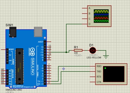
Image1 - Electrical circuit schematic
To perform the reading and verify the microcontroller functioning, an oscilloscope and a virtual terminal are being used, each one connected to the output of the Arduino board in the simulator. It is worth mentioning that there is no need to connect the GND of the board to the GND of the simulation as this is already done internally automatically by the library used in the simulation. After designing the circuit, it is necessary to load a program to the Arduino board to test its operation, this program was made in the Arduino IDE. We must look for the path where this file is located. After being compiled the file is in the “.hex” format.
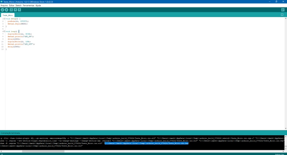
Image2 - Arduino IDE
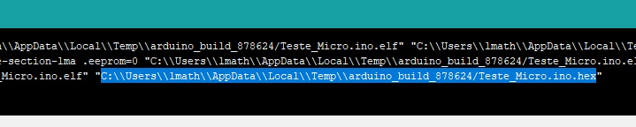
Image3 - Path where the .hex file is saved
After this step, back to Proteus the Arduino is selected and the Edit Component window opened, in the parameter “Program File” we put the path copied previously.
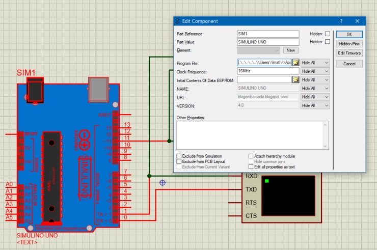
Image4 - Add address in the “Program File” parameter
Activity
With the circuit assembled and the program loaded, the simulation starts, I divided the simulation into three situations that I will measure using a virtual oscilloscope and a virtual terminal.
-
Step up when a logic level pulse 1 is sent.
-
Step down when a logic level pulse 0 is sent.
-
Behavior of the signal when a message is sent over the Serial.
Situations 1 e 2
As you can see in the previous images, the test program is a “Blink LED” program which uses the Serial to indicate the status of the LED, this status is shown in the last line, the green line of the oscilloscope. As expected, the output signal resembles a pulse train because of the constant changing of the LED status.
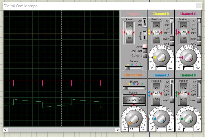
Image5 - Digital Oscilloscope 1
Situation 3
Subsequently, I tried to understand the behavior of the micro serial output, exemplified in the pink line presented in the previous situation, where it is possible to notice some pulses, when expanding the oscilloscope sample, different pulses can be observed in the same output in a triangular shape. It is known that the Arduino makes use of waves in PWM (Pulse-Width Modulation) in this situation, a form of digital signal that makes it possible to obtain analog behaviors by manipulating the duration of each state of high logic level.
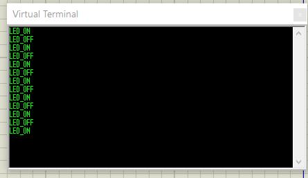
Image6 - Virtual Terminal

Image7 - Digital oscilloscope 2
Practical test
For this activity, I choose to do the tests with an Arduino UNO board available in the laboratory. I used a simple LED transition program with the information in the serial of which LED will be lit. I choose to make a circuit with 3 blinking LEDs, causing a transition effect together with the Serial informing which Led would be on. Different from the simulation in Proteus, where I made a circuit with an LED and an activation button.
Image8 - Pratical test
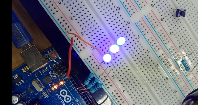
Image9 - LEDs on protoboard
To check its operation, I positioned the oscilloscope probe on the Arduino’s RX/TX terminals using jumpers.
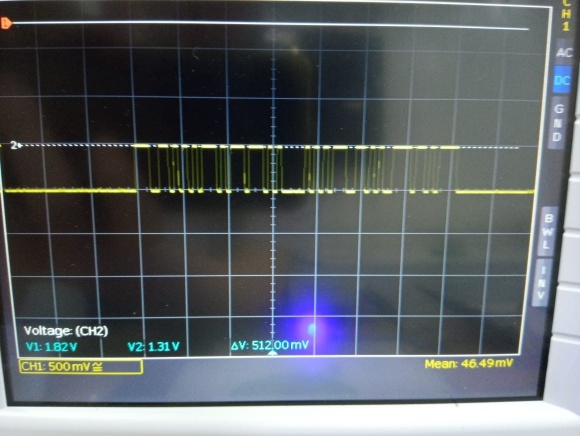
Image10 - Real Oscilloscope
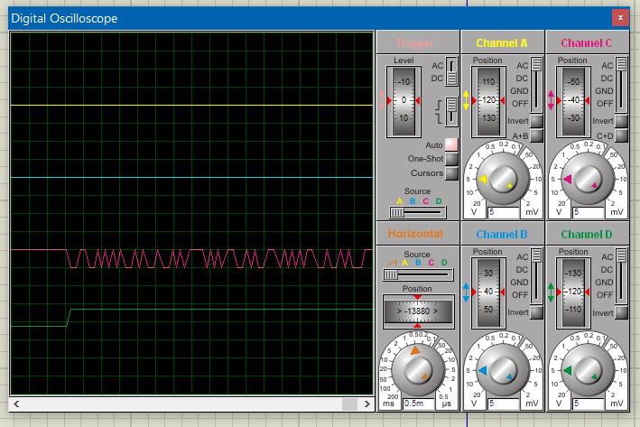
Image11 - Oscilloscope Simulation
The waveform in the real oscilloscope is a little bit different from that observed in the simulation and is more like a pulse train because the sampling rate of the real oscilloscope is optimized in comparison to the simulated oscilloscope in Proteus.
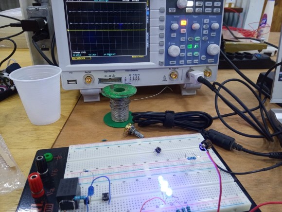
Image12 - Circuit used for the test
Individual assignment
- redraw an echo hello-world board,
- add (at least) a button and LED (with current-limiting resistor)
- check the design rules, make it, and test it.
In the Electronics Production assignment, I described the necessary steps to design and produce a PCB layout using Proteus software (redesign and produce an in-circuit programmer). In this week assignment I will briefly show these steps again using the ATtiny45 electrical diagram in the figure below as a reference and adding a Led and a button to the circuit.
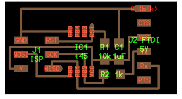
Image13 - Board Design
Before I started, I decided to study the ATtiny45 Datasheet to understand the pinout configuration and learn which outputs was the correct ones to connect the button and the Led.
It was a good exercise to find this info in the Datasheet.
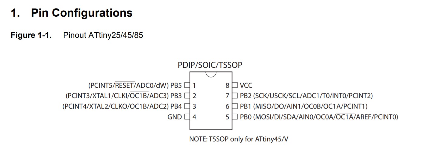
Image14 - Pin configuration
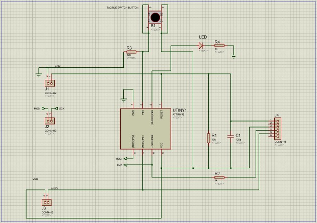
Image15 - New PCB schematic
Due to Pandemic situation I had difficulties in getting SMD components, only the ATtiny45 was SMD the others components was all PTH. Because of that in the SRM-20 machine we add one more step to prepare the holes of the board.
As can be seen in the image, there is a short circuit between some terminals of the push-button, this can be done because internally these pins are already connected, I made the connection because in Proteus it would make easy to designing the PCB.
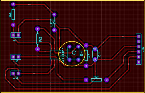
Image16 - PCB on ARES
In the situation without the short circuit, it would be necessary to make adjustments to the schematic, in my case, just rotate the push-button would be enough, however I added the button with LED only after making the base circuit, and rotating the components at that time meant that there was not enough space, so I opted for the first solution, integrating the button’s internal short circuit to facilitate adjustment.
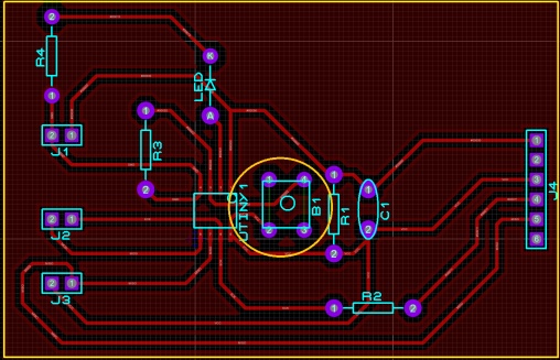
Image17 - Button
Due to the schematic short circuit of the Button component, the circuit design of the PCB became easy to implement
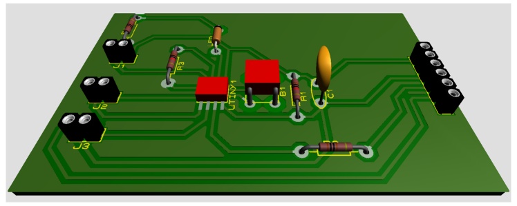
Image18 - Design of the circuit
This was the design of the board, following these production rules:
Image19 - Production rules
Ilustration
With the same steps done in the Electronic Production Week I add the Sumaúma name in the PCB

Image20 - PCB with Sumaúma printed
MOD configuration
For the MOD configuration, I tried to better study some functions that I already knew and explore new ones
Output
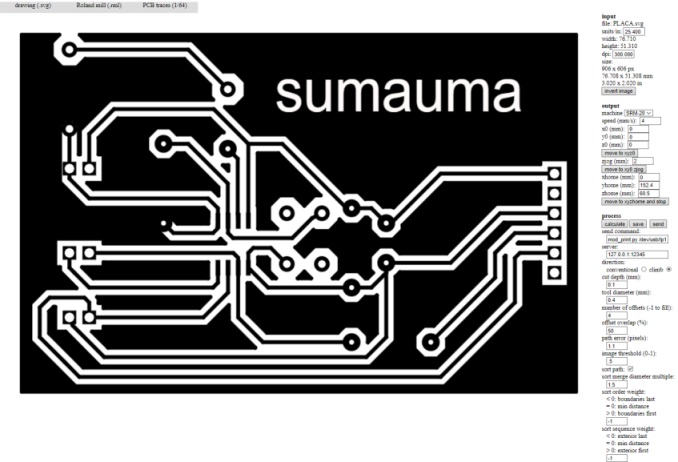
Image21 - MOD configuration
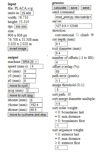
Image21.1 - MOD configuration 2
a. x0, y0 and z0: Position of the origin axis of the “rml” file within the axis defined on the machine (SRM - 20)
b. zjog: distance/height traveled on the Z axis when moving from traces to traces, on the module this traveling is indicated by the red lines on the image bellow.
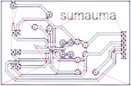
Image22 - Traces
c. xhome, yhome and zhome: When the machine finishes production, the drill will be moved to the coordinates indicated in that configuration. If set to (0, 0, 0) you risk breaking the drill at the end of the process. It has occurred to me a few times in previous projects, but now I have been able to correct it.
d. number of offsets: Indicates the number of layers that will be milled, it is possible to remove unnecessary islands as indicated in the image below, as I chose to choose only 1 layer (the image on “home” is with only 1 layer).
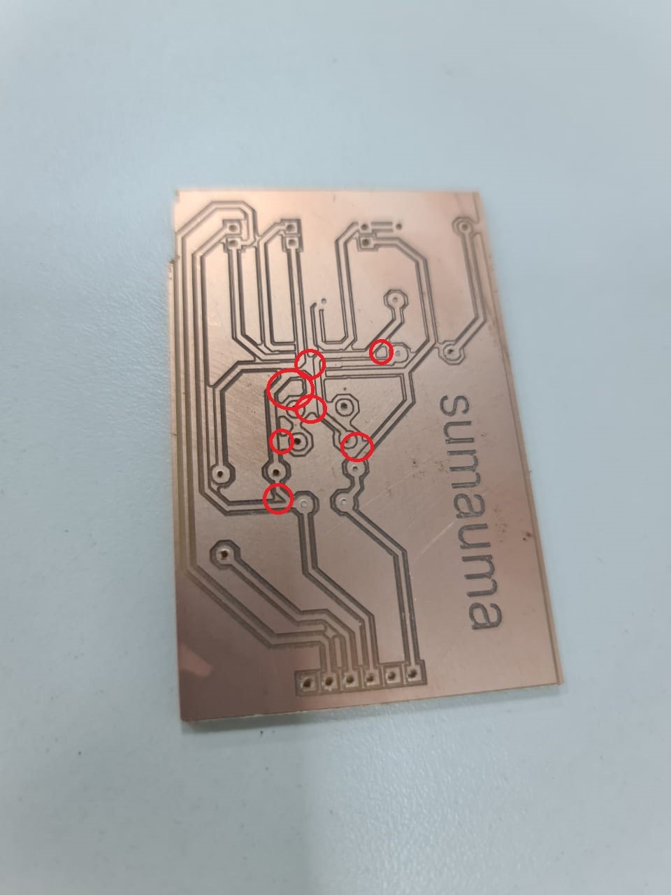
Image23 - Note: Because I used only 1 layer in the offset configuration, these marked regions were kept on the board. By increasing the value to 3 or more layers, these regions would have been removed in the process.
e. Offset overlap(%): Indicates the separation of each offset layer, depending on the tool diameter and offset number, different values could take the same result.
f. Path errors (pixels): Indicates the interval between the pixels of the circuit mask for the generation of the movement vectors of the drill, I did not do the practical test by varying this value so I cannot say how this would interfere in practice.
g. sort path: by checking this option, the process is optimized by using vectors. Unchecking the option, the process is done line by line, as shown in the image below.

Image24 - Path errors(pixel): 0.1
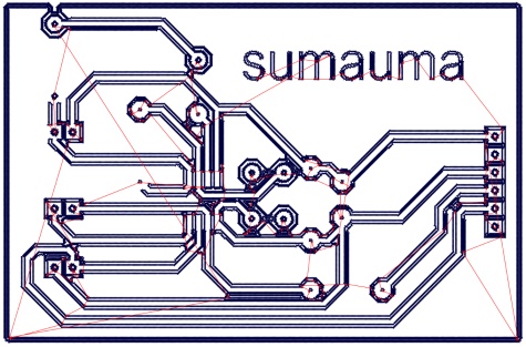
Image24.1 - Path errors(pixels): 0
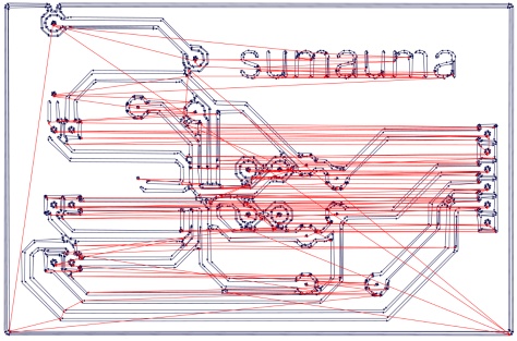
Image24.2 - Sort path Unchecked
Once the “rml” file is prepared, simply upload it to the machine and select cut to start production.
In total, 3 processes were carried out:
- Traces
Settings: - x0, y0 e z0: (0, 0, 0) - zjog: 2 mm - xhome, yhome e zhome: (0, 152.4, 60.5) - Cut depth: 0.1 mm - Tool diameter: 0.4 mm - Number of offsets: 1 - Offset overlap(%): 50% - Path errors (pixels): 1.1 - Sort path: checked
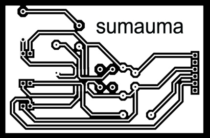
Image25 - Trace mask
Image25.1 - Trace path
- Holes
Settings:
- x0, y0 e z0: (0, 0, 0)
- zjog: 2 mm
- xhome, yhome e zhome: (0, 152.4, 60.5)
- cut depth: 1.6 mm
- tool diameter: 0.4 mm
- number of offsets: 1
- Offset overlap(%): 50%
- Path errors (pixels): 1.1
- sort path: checked
Note: In this process, I set the mill speed to 10%~20% so the quality of holes is good enough and the process doesn’t damage the board.
Image26 - Hole mask
Image26.1 - Hole path
- Edge
Settings:
- x0, y0 e z0: (0, 0, 0)
- zjog: 2 mm
- xhome, yhome e zhome: (0, 152.4, 60.5)
- Number of offsets: 4
- Offset overlap(%): 50%
- Path errors (pixels): 1.1
- Sort path: checked

Image27- Edge mask

Image27.1- Edge path
Final PCB
Before soldering the PCB I did the circuit continuity test of the PCB, everything look fine.
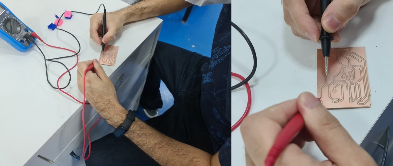
Image28- Continuity test
I prepare de component list and check with the multimeter if all components are OK
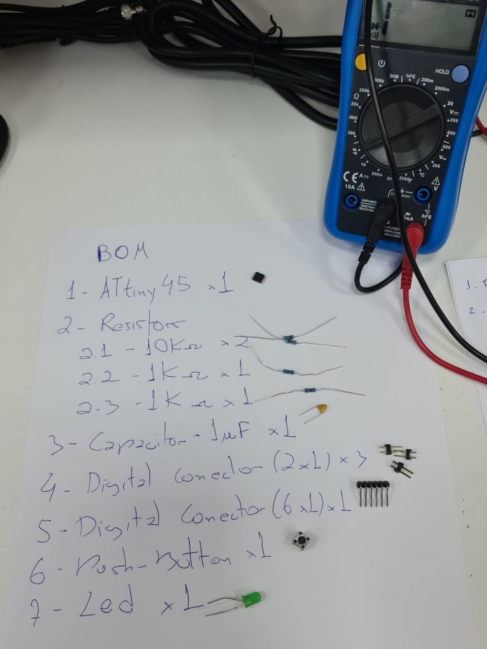
Image29- Components List
So after checking the circuit continuity and the component I started soldering the PCB
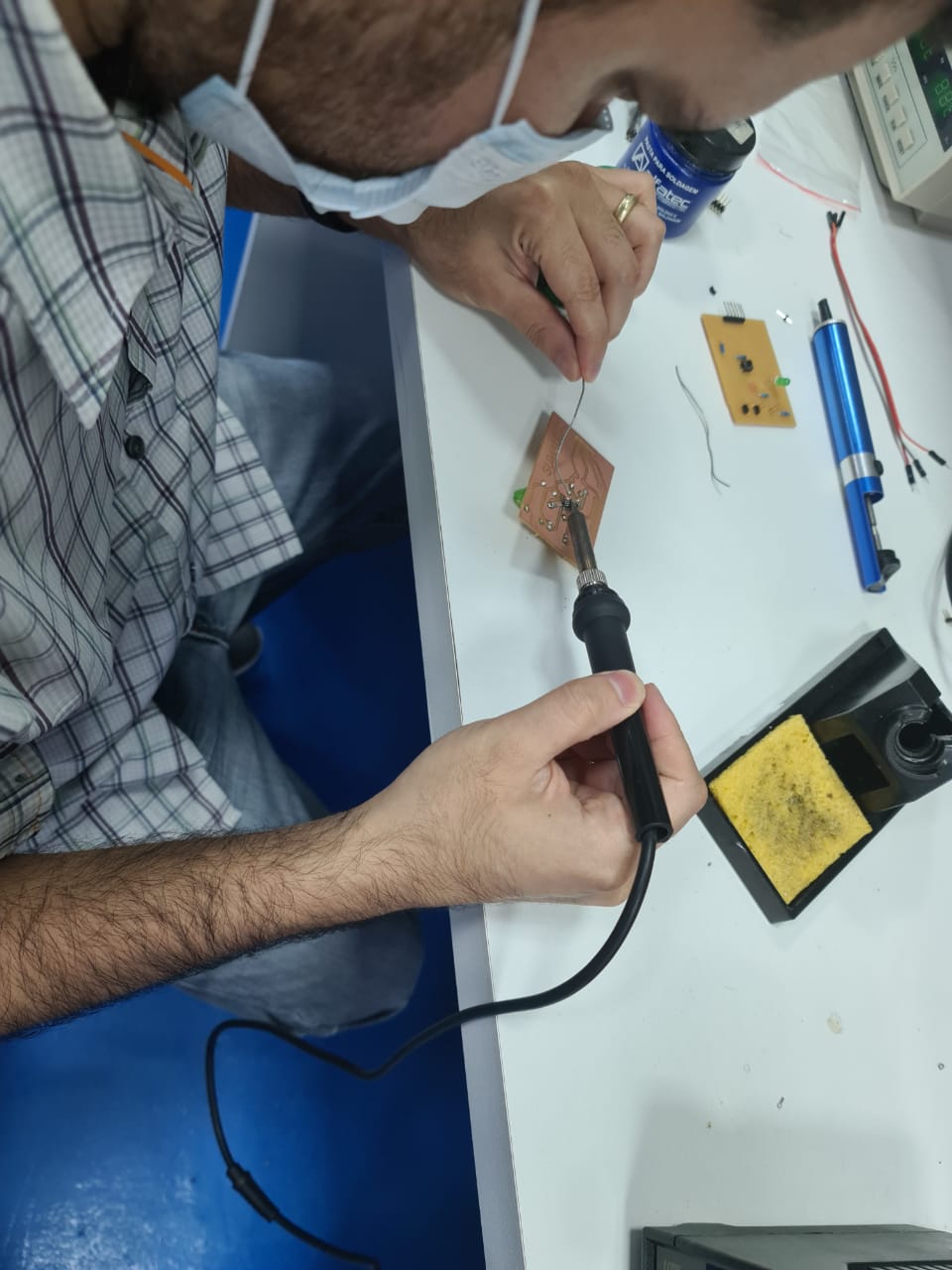
Image30- Soldering
The result of the soldering can be see below.
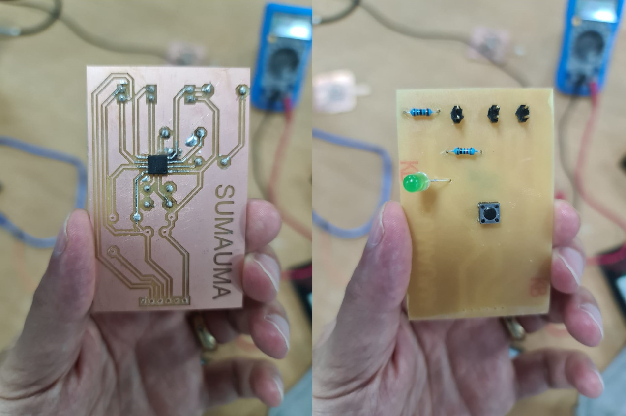
Image31- Result
Programming
Due to some problem in the electronic production assignment week the in programmer board still not working properly, and using spiral management I decided to programming of ATtiny45 using Arduino IDE, it is easy to install. After opening Arduino IDE, it was necessary to do the following steps:
I learn this procedure by watching three youtube nice videos 1, 2, 3.
- Click on file and then on preferences.
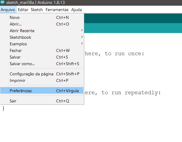
Image32- Preferences
- Add the library URL.
- Click OK.
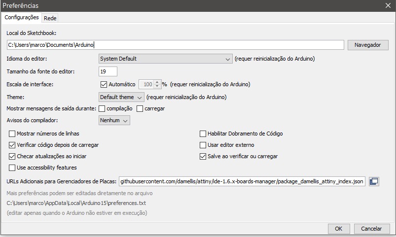
Image33- Add library
After adding the URL, it is necessary to go to “tools” and then select “card manager”.
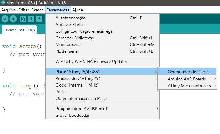
Image34- Card Manager
In the “card manager” window, we type the model of the card we want to add, in my case it is ATtiny, and then confirm the installation of that card, in my case the install option is not available because I already installed it.
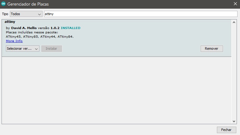
Image35- Card Manager window
Arduino as a ISP programmer
To load the code of ATtiny45 using ISP, first is necessary to turn the Arduino into an ISP programmer, to do that I followed the steps below:
-In archives we click on examples and select ArduinoISP.
Image36- ArduinoISP
This will open a file that will be uploaded to the Arduino and will allow it to work with an ISP programmer.
Image36- ISP programmer
Before writing the code, it is necessary to check if the IC (ATtiny45) is selected right and if the Arduino COM port is enabled. The Arduino used as an ISP programmer was the Arduino UNO and was on the COM 8 port as shown below.
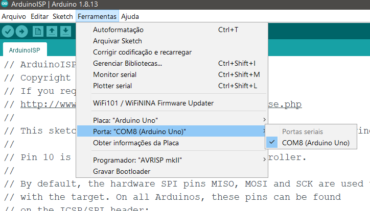
Image37- COM8
IDE Arduino for ATtiny45
With the card installed, the board model is selected in “tools” and then in ATtiny Microcontrollers. In this activity an ATtiny45 was used which corresponds to the first option.
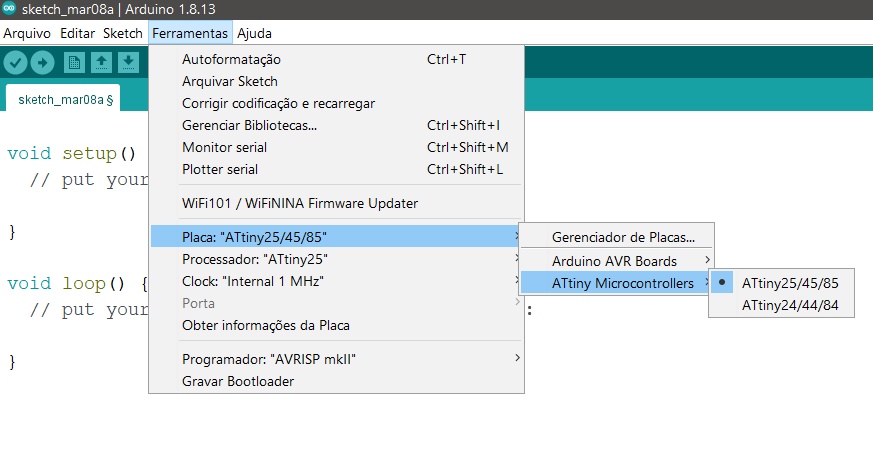
Image38- Selecting ATtiny45
It is necessary to go to “tools” and change the processor to ATtiny45 too.
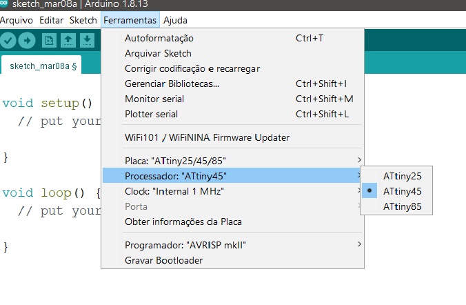
Image39- Selecting ATtiny45 2
Again, in “tools”, it is necessary to change the clock to External 20 MHz.
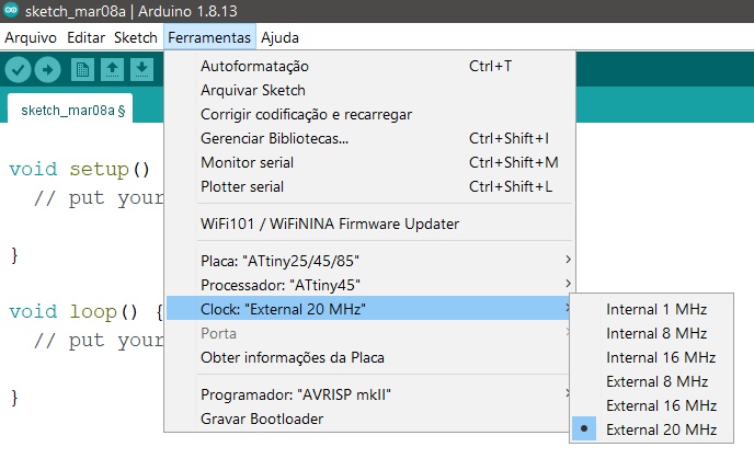
Image40- Selecting External 20 MHz clock
Finally, the programmer was modified to Arduino as ISP because ISP communication was the way used to program our ATtiny45.
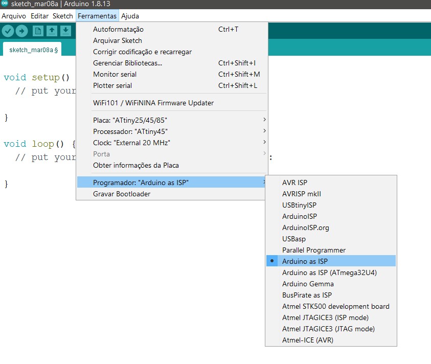
Image41- Selecting ArduinoISP as the programmer
Now we are ready to do the programming and the connection of the Arduino with ATtiny45:
- First the Arduino and ATtiny45 ISP pins were recognized.
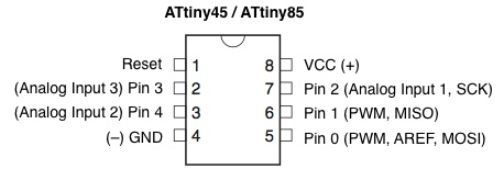
Image42- ATtiny45 pin configuration
Image42.1- ATtiny45 pin configuration 2
Table with connection for SPI pins.
| Arduino UNO | ATtiny45 | Description |
|---|---|---|
| GPI012 | Pin1 | MISO |
| GPI011 | Pin0 | MOSI |
| GPI013 | Pin2 | SCK |
| GPI010 | Reset | SS |
It is necessary to connect the Arduino’s VCC and GND pins to the ATtiny45 to be able to power it. After connecting the SPI and power we will move on to programming and testing the operation of ATtiny45.
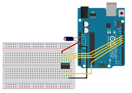
Image43- Connections on protoboards
Now I am ready to make some tests :)
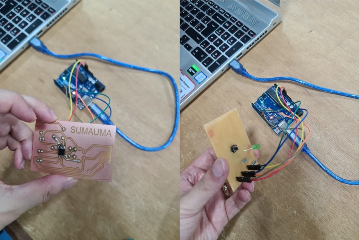
Image44- Arduino ready
Button Pressed to lightup the LED.
In this program an LED were used, and it will light up when a button is pressed and go out when it is not being pressed. The code has the int’s led and button that represent the ports of the ATtiny45 where the LED and the Button are connected, as the button is a value that will be read by the Arduino then it is declared as an input and as the led will be a value written on the Arduino pin then it is output. DigitalRead was used to read the pin value of the button and turn the led on or off.
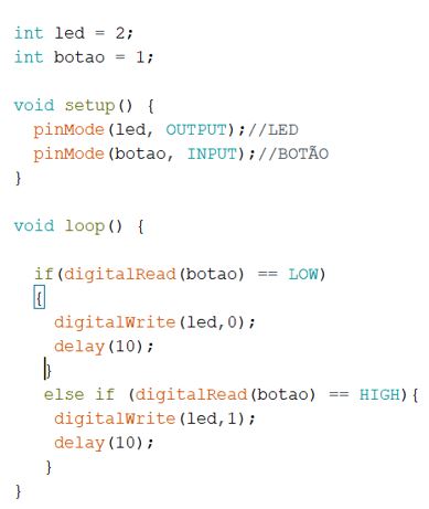
Image45- Code
Blink test
To do the Blink test, the Arduino sample model was used, which is available in “files” as shown in the image below.
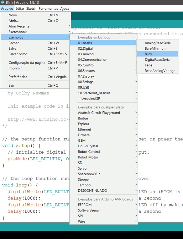
Image46- Blink test sample
In this code, it is only necessary to identify the pin where the LED is connected and modify it, in my case it is on pin 2 of ATtiny45.
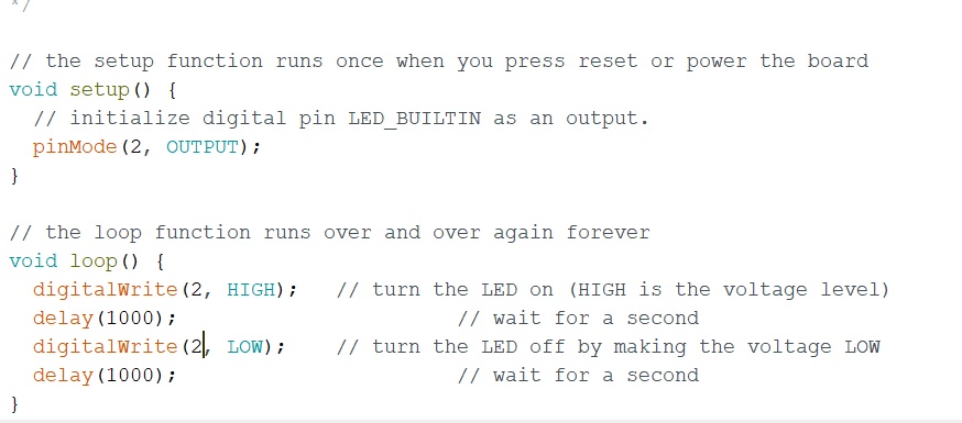
Image47- Blink code
ECO test
After the Blink test, I will do the ECO test with the available code.
Note: Unfortunately, in the output week, the pcb burned, but in that same week I made a new board and used a power supply to power the PCB.
Conclusions
This week I learned a lot about Electronics Design, it was the most challenging week of the course so far.
- All the files done in this week assignment can be find in the repository