Electronics Design
———-
Group assignment:
- Use the test equipment in your lab to observe the operation of a microcontroller circuit board (in minimum, check operating voltage on the board with multimeter or voltmeter and use oscilloscope to check noise of operating voltage and interpret a data signal)
- Document your work ( link to group assignments )
Individual assignment:
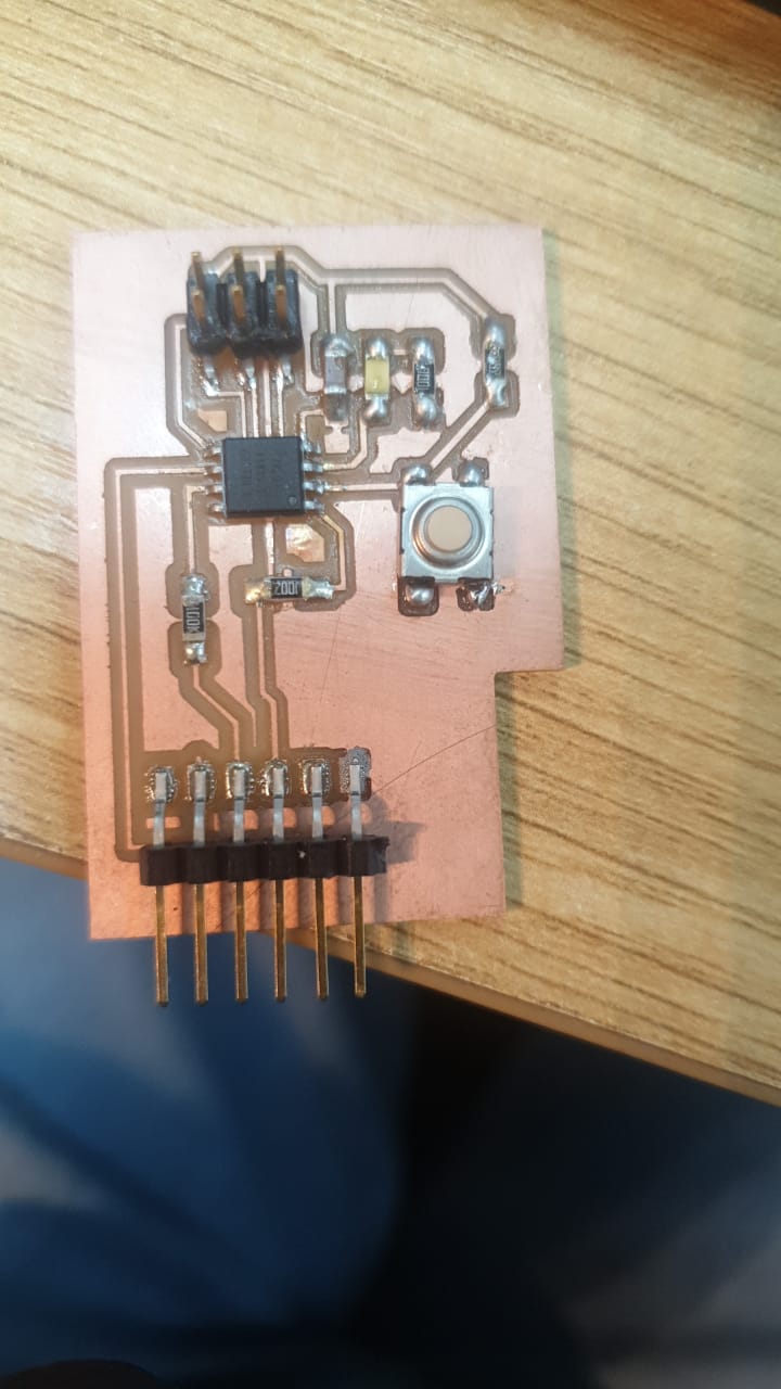
- Redraw one of the echo hello-world boards or something equivalent, add (at least) a button and LED (with current-limiting resistor) or equivalent input and output, check the design rules, make it, test it.
One of the reasons I joined fab academy is to learn electronics design, so this week is a chance to develop my electronic skill I am so excited about the number of things I am going to learn here.
in this week lecture Nail showed us some of the software for electronics design, one of the top software that he recommended is Eagle and Kicad so i will start by experimenting booth of them then decide which one iam going to stick with and in order to do the comparison i will spend one houre on each software
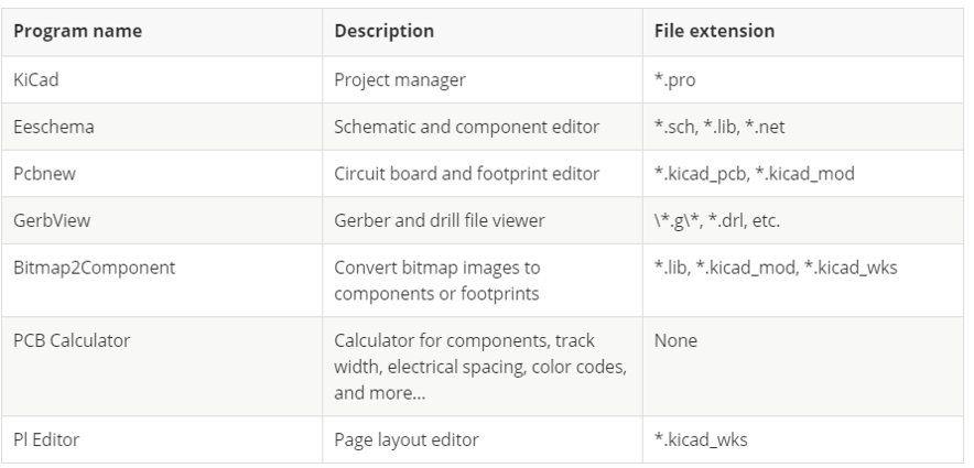
1- KiCad EDA
KiCad is an open-source software tool for the creation of electronic schematic diagrams and PCB artwork. Beneath its singular surface, KiCad incorporates an elegant ensemble of the following stand-alone software tools:
Downloading and installing KiCad
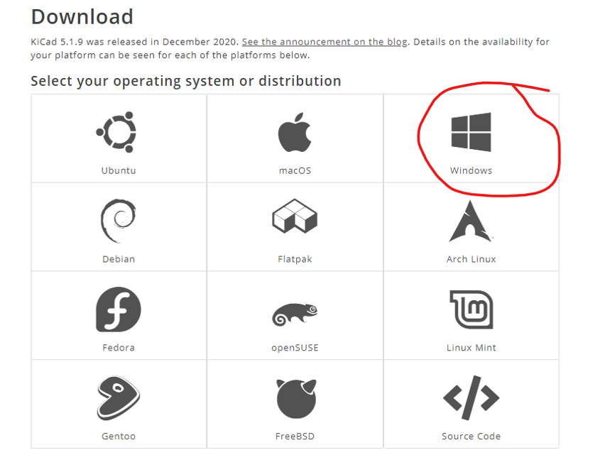
KiCad runs on Cross-platform it works on GNU/Linux, Apple macOS and Windows. You can find the most up to date instructions and download links Here, for me i have windows device so i downloaded windows version.
After Downloading the software now its time to install it, the software require 5 Gb so make sure you have enough space in your hard drive, for me I don’t have that space on my C drive so I installed it on the D drive
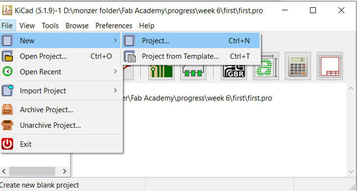
Start new project
Now you are ready to lunch the software, from the main menu start a new project
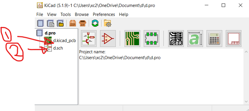
once you open a new project KiCad is going to create tow file for you
- PCP layout Editor
- Schematic Layout Editor
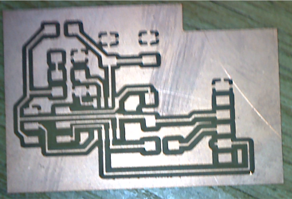
Choosing the hello-world board you can find them HERE
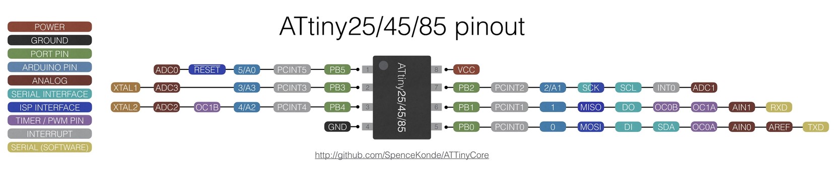
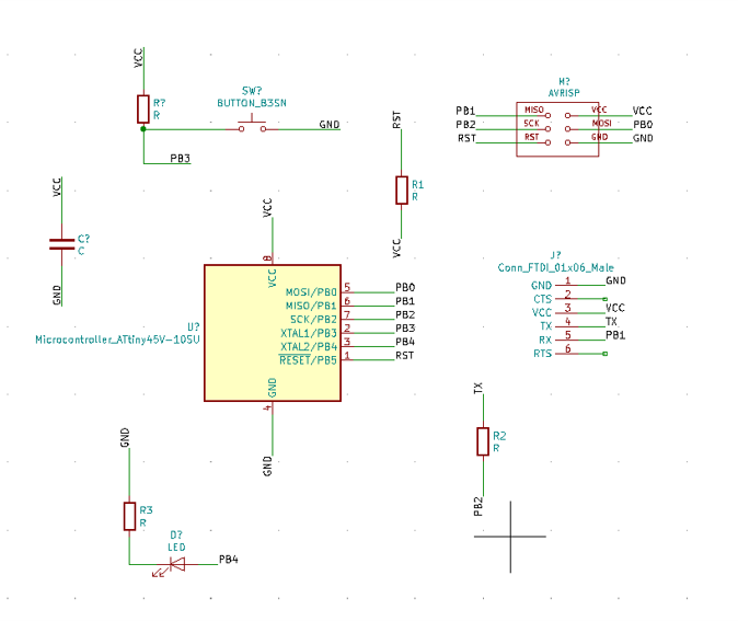
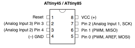
Before starting to drow your circuit you need to choose the hello-world board that you want to work with, for me the chip that i have is ATtiny45
Next is to check the list of component and instruction of how to use it
so I downloaded all the files and saved them in my laptop the component are :
- ATtiny45
- 2x3 pin-Header AVRISPSMD
- LED
- Push-button
- FTDI-SMD-Header
- Capacitor 1uF
- Resistor 10K Ohm
- Resistor 1K Ohm
- Resistor 240 Ohm
- Resistor 100 Ohm

Then i looked for the datasheet and pinout of the chip to understand it better i got the pinout frome Here and find other information from HERE
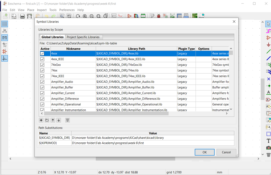
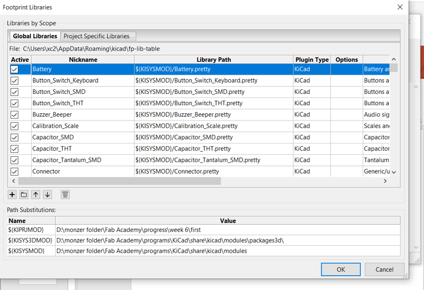
Next you have to download the fab liberary for KiCad HERE
After downloading the library you have to upload it to Kicad liberary in order to be able to use them in the schematic
Adding Symbol to Schematic
By clicking a on the schematic board you can add new symbol or just Click A and then search for attiny45 and by right clicking you can see the datasheet and specification of the symbol
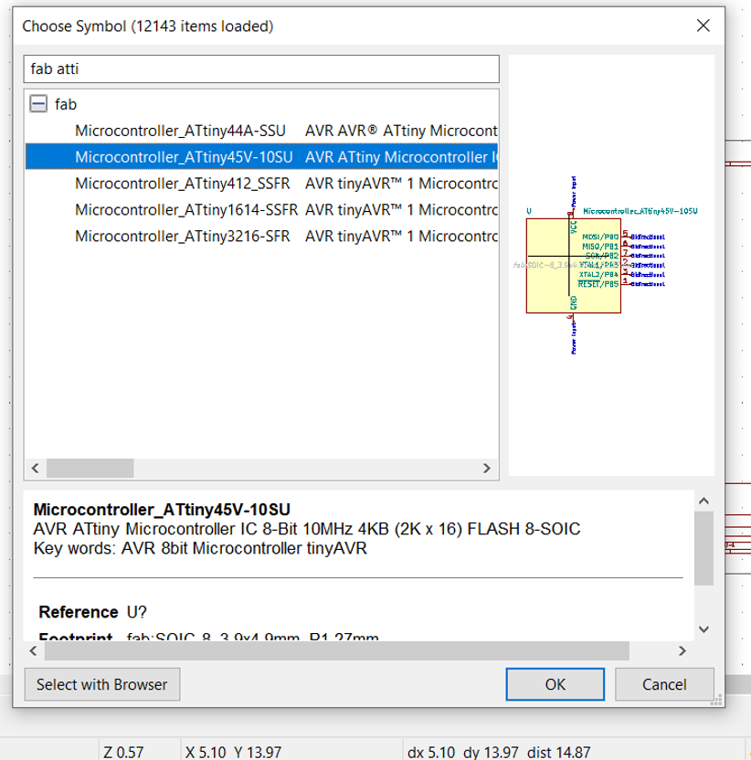
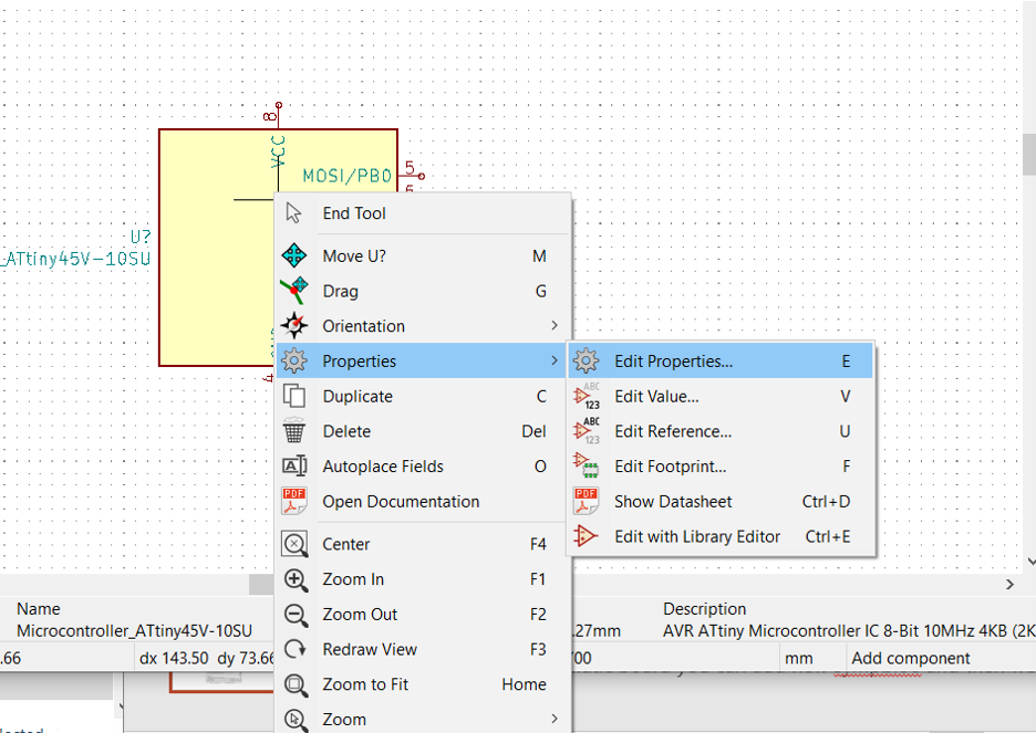
Adding Symbol to Schematic
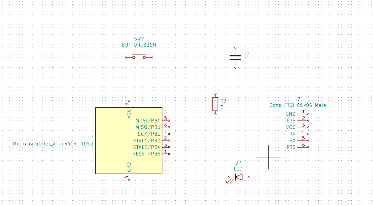
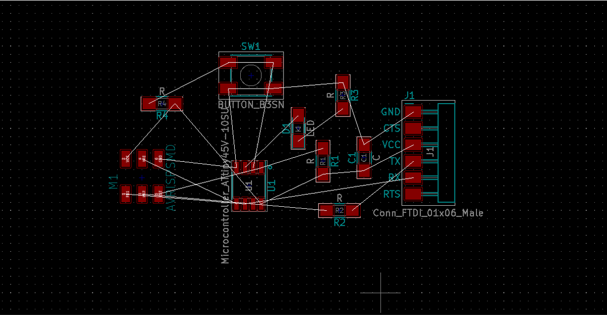
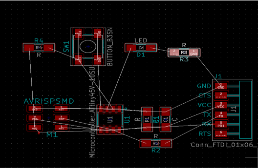
Now I added all the component that on the list, then as per the assignment for this week i added a button and a led and a resistor
Wiring thigs up
it was Fun Wiring the componnent together it reminded me How LAB View Programming look like,
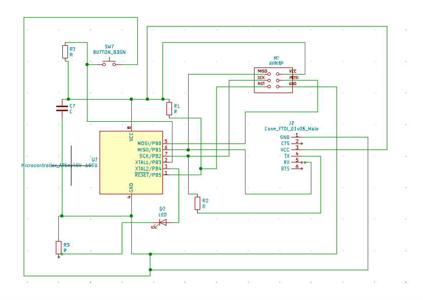
Cleaning the Schematic By Labeling
Even though I have enjoyed wiring the schematics still its a process that take time and its not easy to be read by other, So I Decided to try labeling the component to organize the schematic.
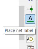
To do the Labeling you need to click the (A) symbol found on the right side bar
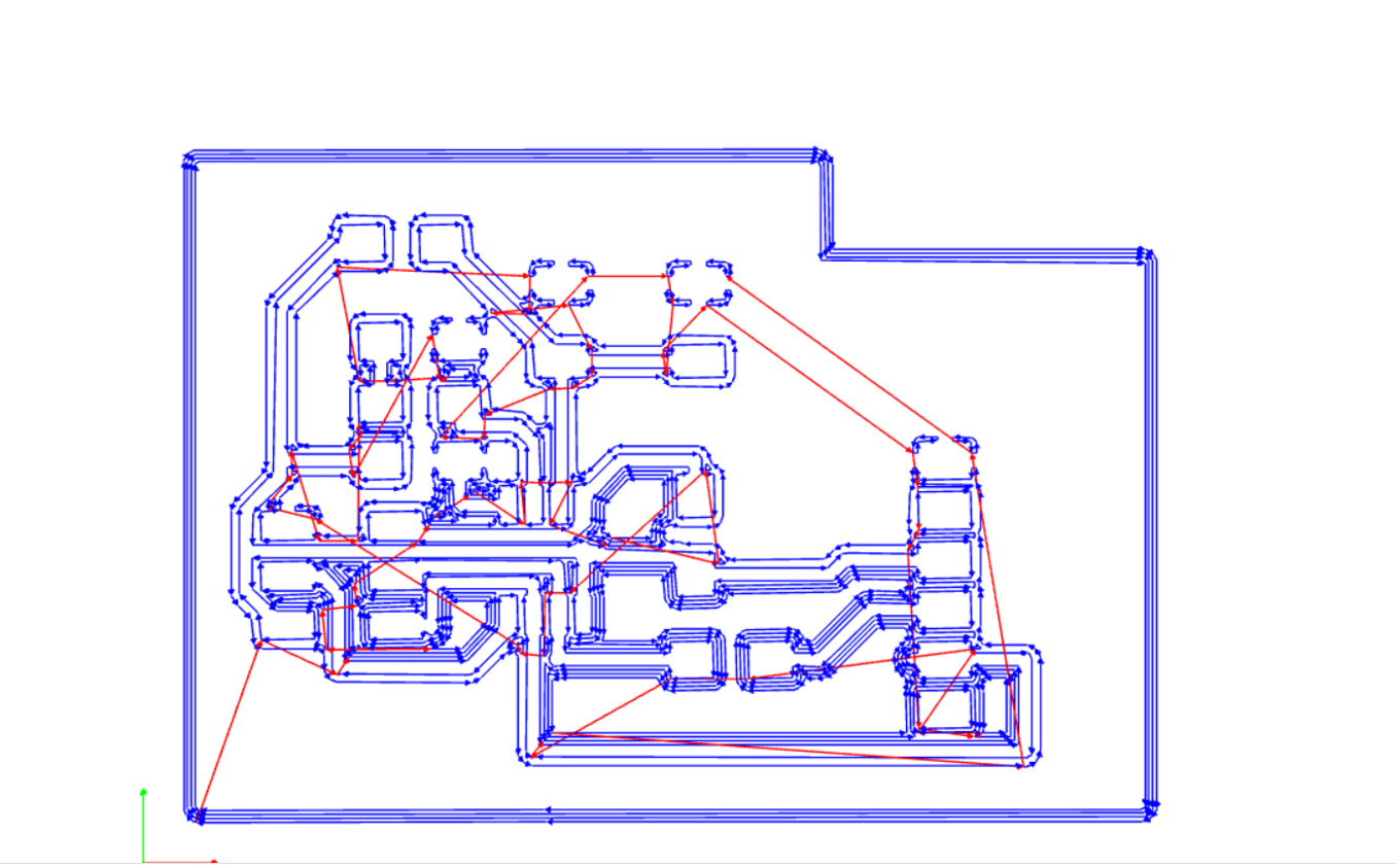
This is the schematic after organize it with the labels
Now the schematic look cleaner and readable.
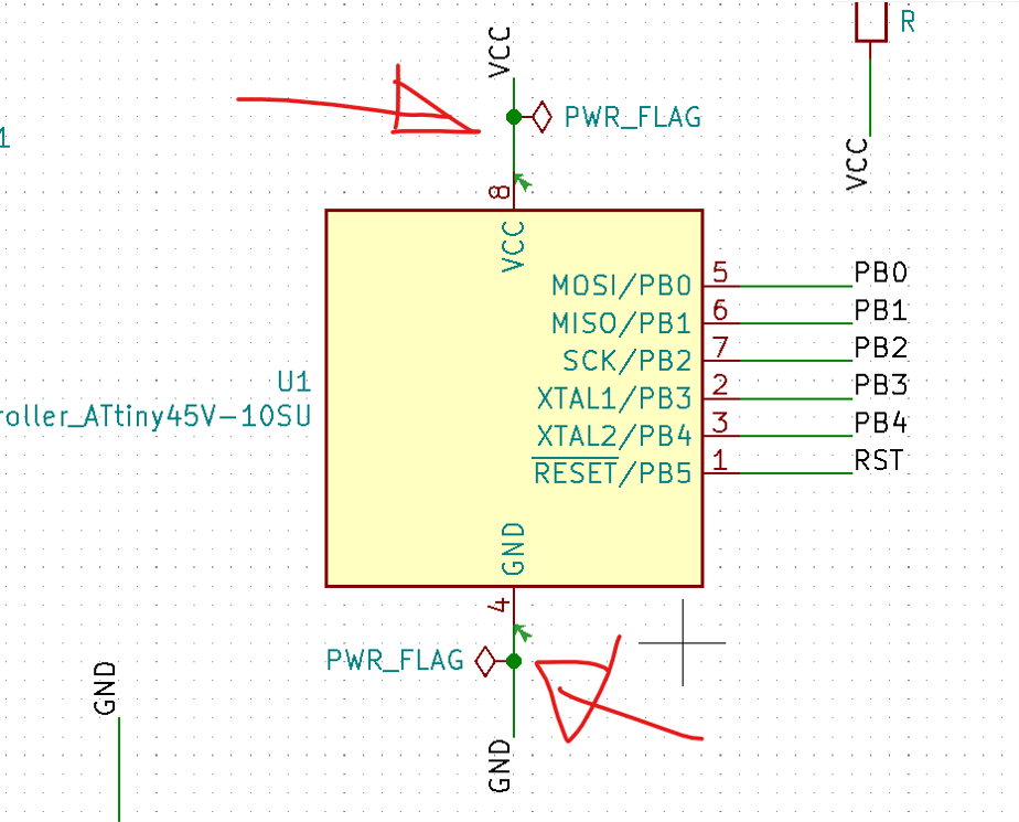
Test the connection with electric rule
By clicking the bug symbol we can run an electric test rule to make sure every thing is good, that test rule is going to check if there is a wire wish is not properly connected or a pin without a connection This
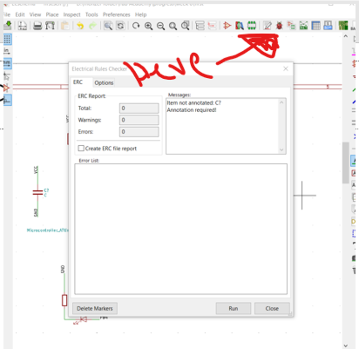
Analyzing the Problems
After running electric rule test tow errors cam out
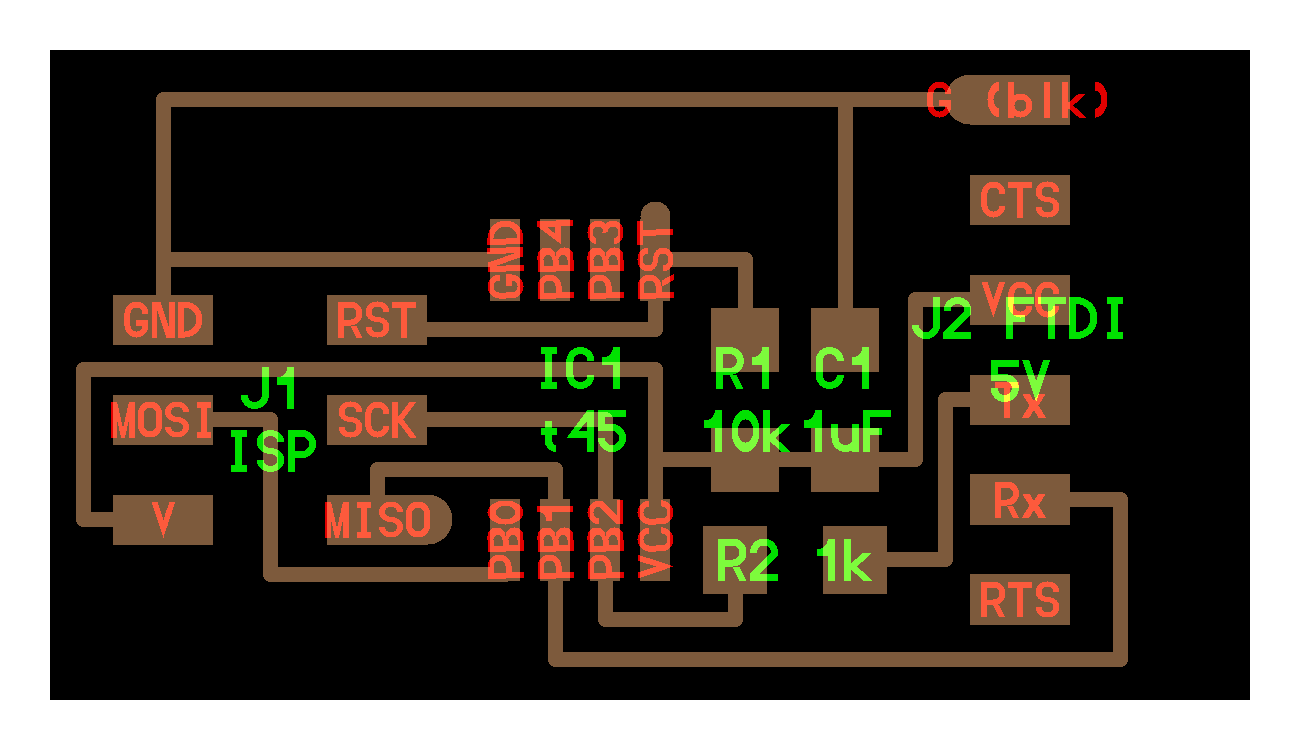
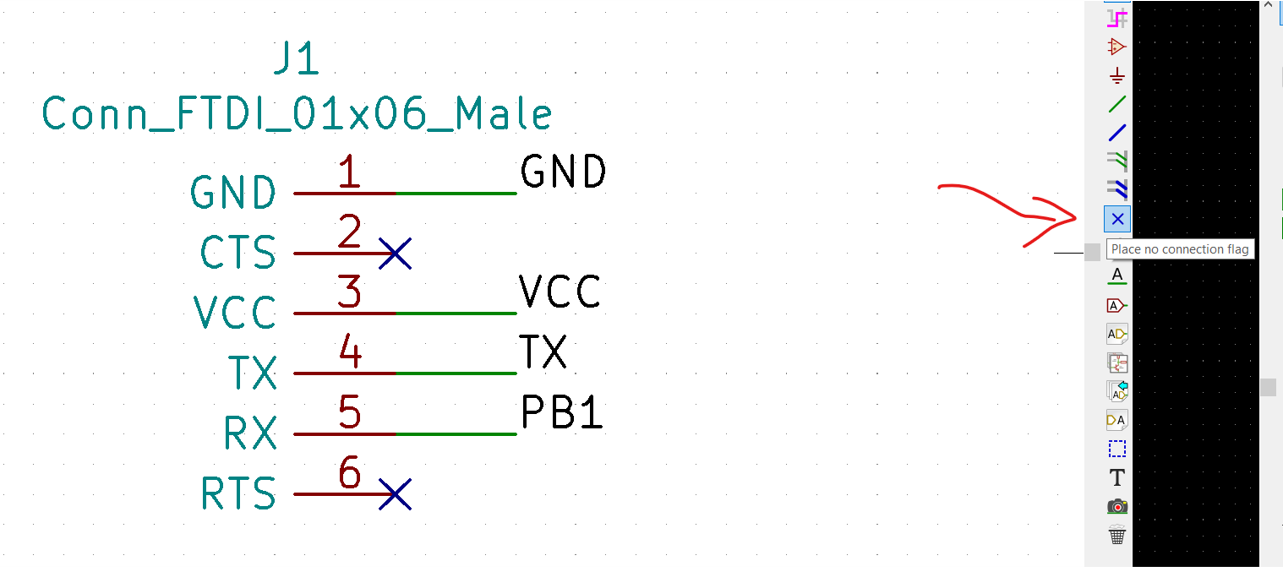
- there is no connection on pin 6 and 2 on J1 ( FTDI connector )
- Power input of pin 4 and 2 ( GND and VCC ) on ATtiny45
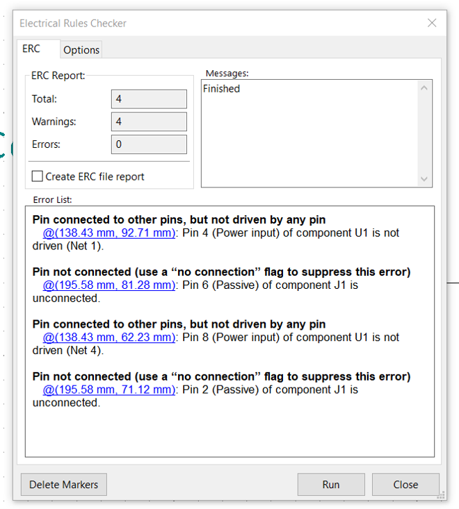
Fixing Schematic Errors
- You Have make sure that any pin in the schematics are in use, and if there is un used pins you have to tag them with no connection Tag
- KiCad Needs to know where is the power are coming from so you need to tag the Power pins ( GND and VCC ) with the power tag
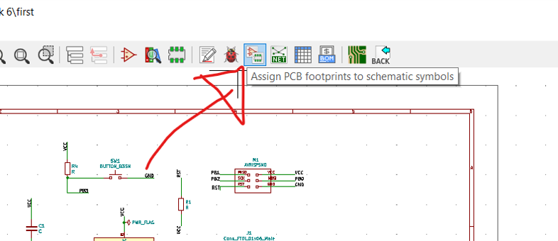
Assigning Foot Prints
Next is to assign PCB foot print for the component on the schematic.
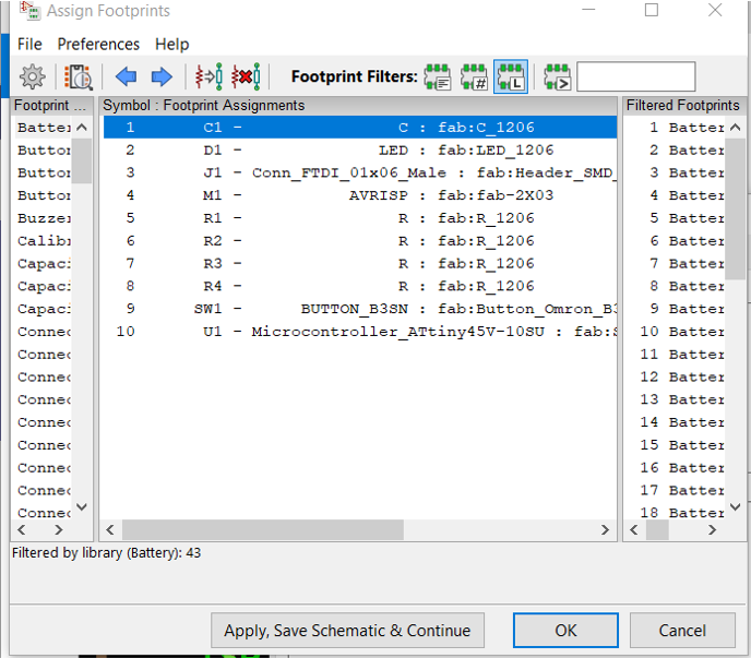
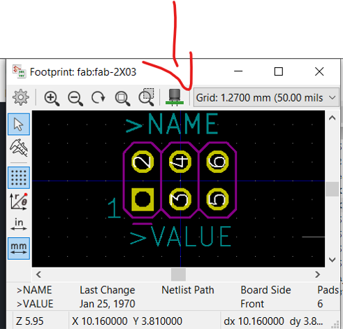
Checking Foot Prints
I had a doubt about ( AVRISP ) that the one I am using is not correct so when I right clicked and viewed foot print I notice the difference
- AVRISP are made for go-through pins
- AVRISPSMD is for the PCB layout, this is what we want
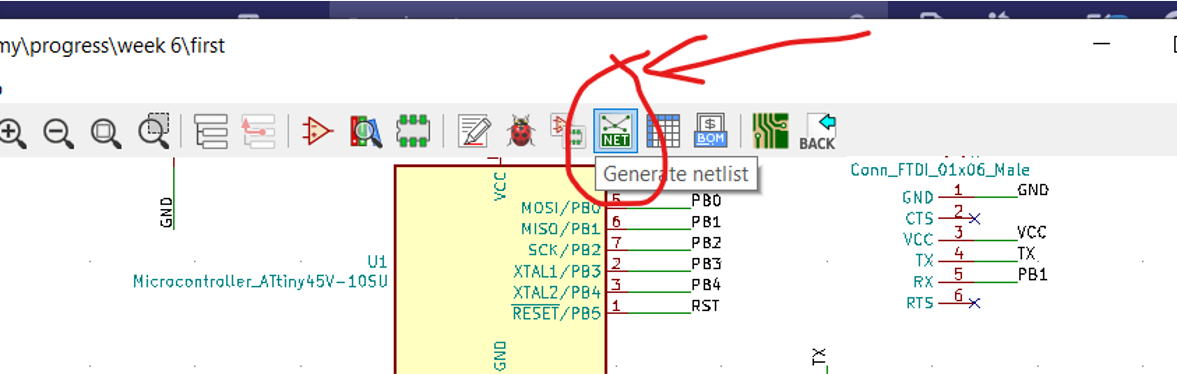
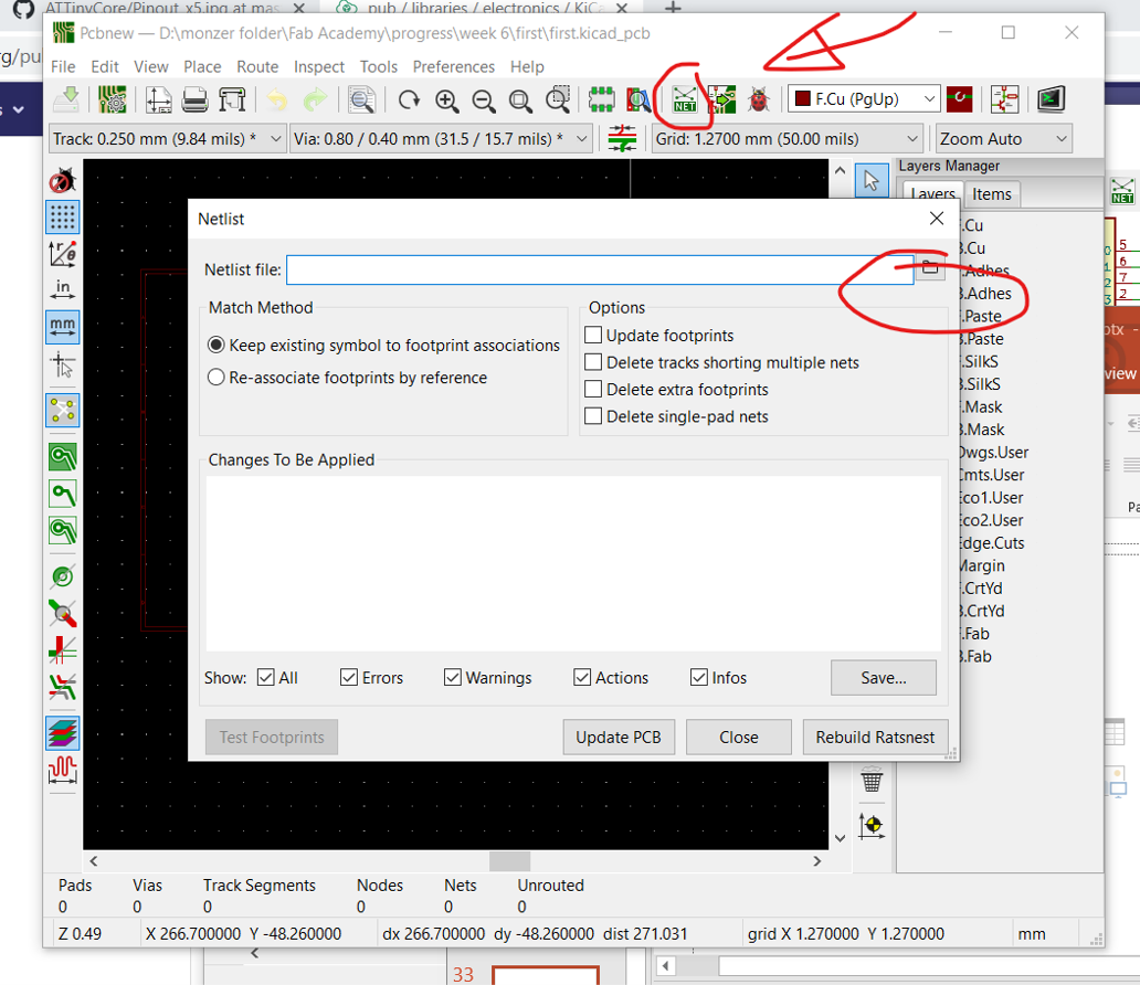
Generate the netlist
next is to generate the netlist by clicking the button showing the picture below, then save the netlist file in the project directory
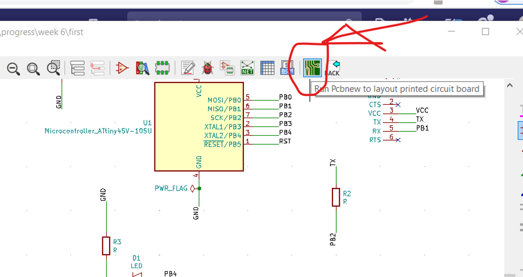
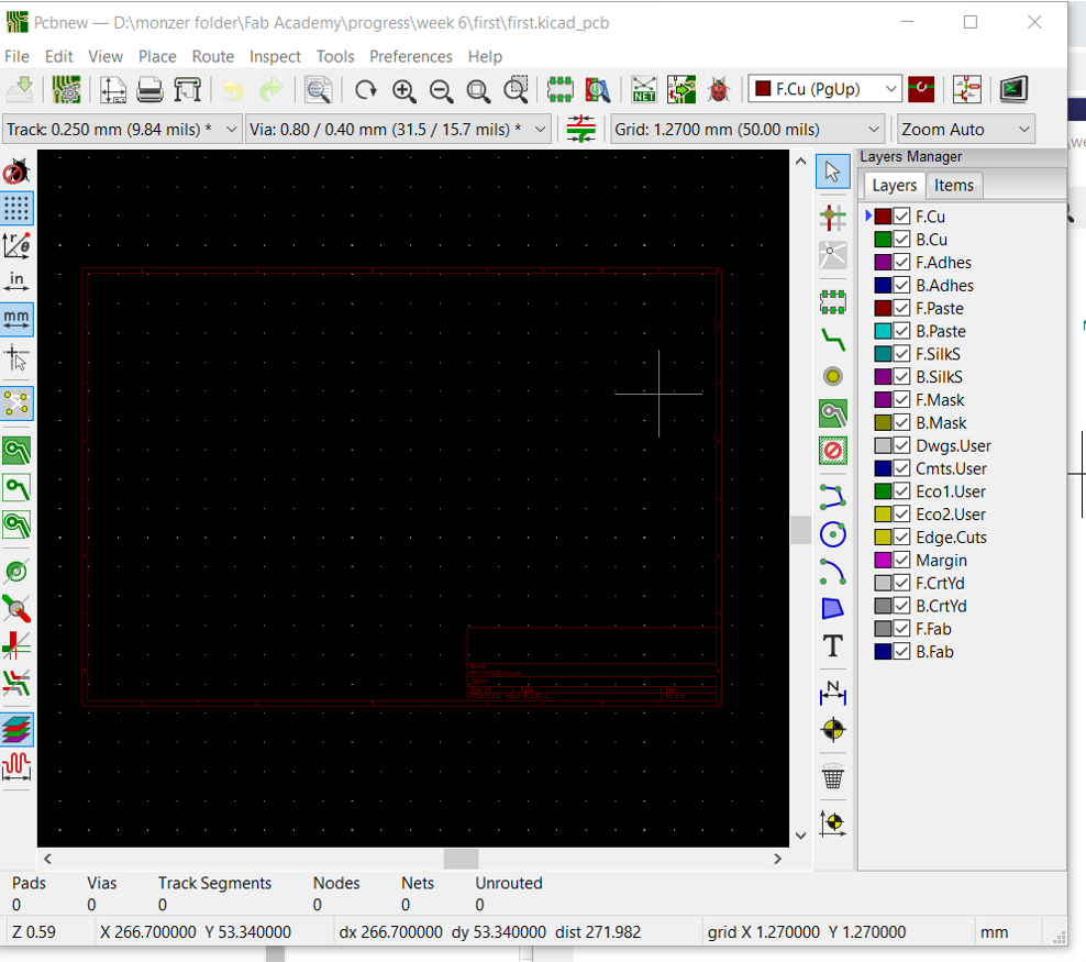
Run PCBnew layout
next to click the pcb button next to the netlist button, in order to layout the component to printed circuit board
Load the netlist
now you have to load the net list from the file that we saved to in the previous step, then click update pcb
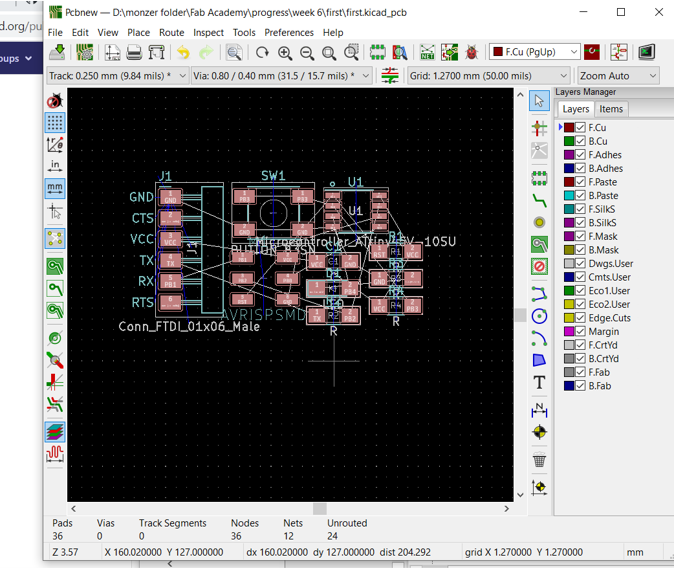
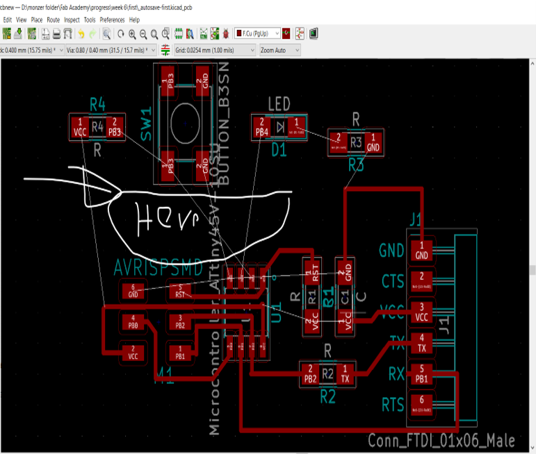
loading the component
past the component in the middle of the screen, you can zoom in and out with the mouse Crouser, notice that the component are connected with this wire, try to organize it first to reduce intersections, by click R button in the keyboard you can flip the component
Edit Trace size
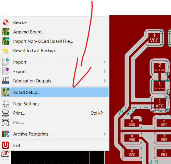
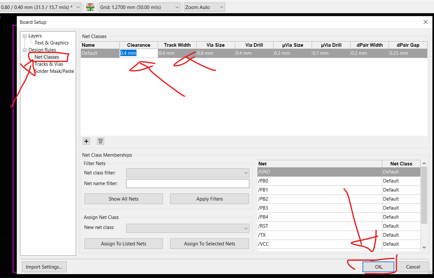
now edit the trace according to your machine and according to the bit that you are using to mill, first go to File , then board setup then chose net classes , edit the clearance and Track width, the rest keep it as it is
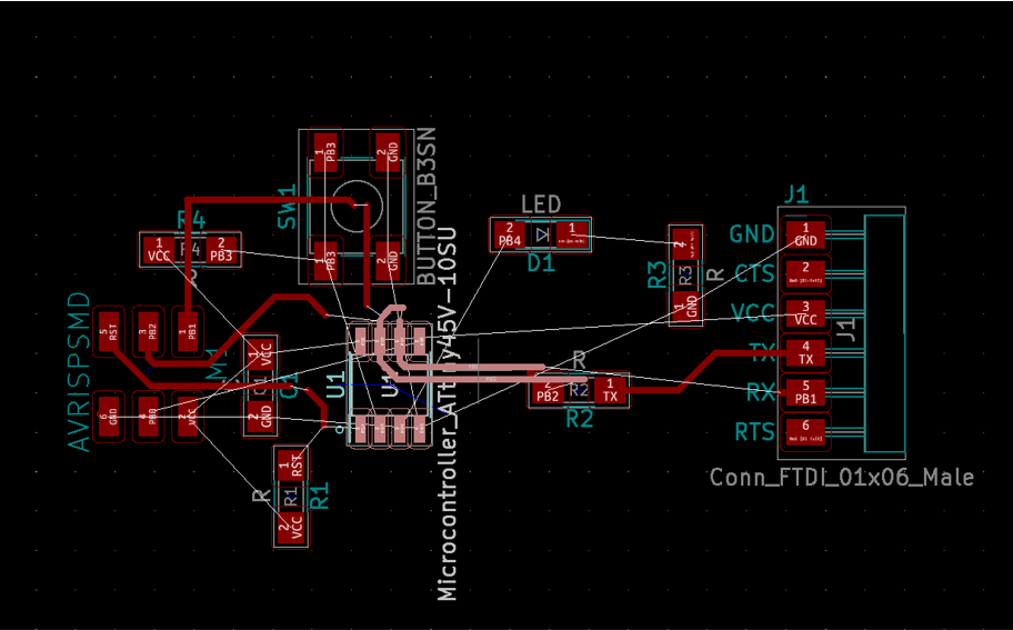
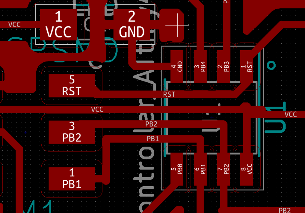
Connecting Traces
After spending one hour trying to figure out how to connect them together without intersection, i found that its not an easy job, so I decided to go to sleep and try again tomorrow.

Next day enthusiasm
The second day I came with enthusiasm to get things done

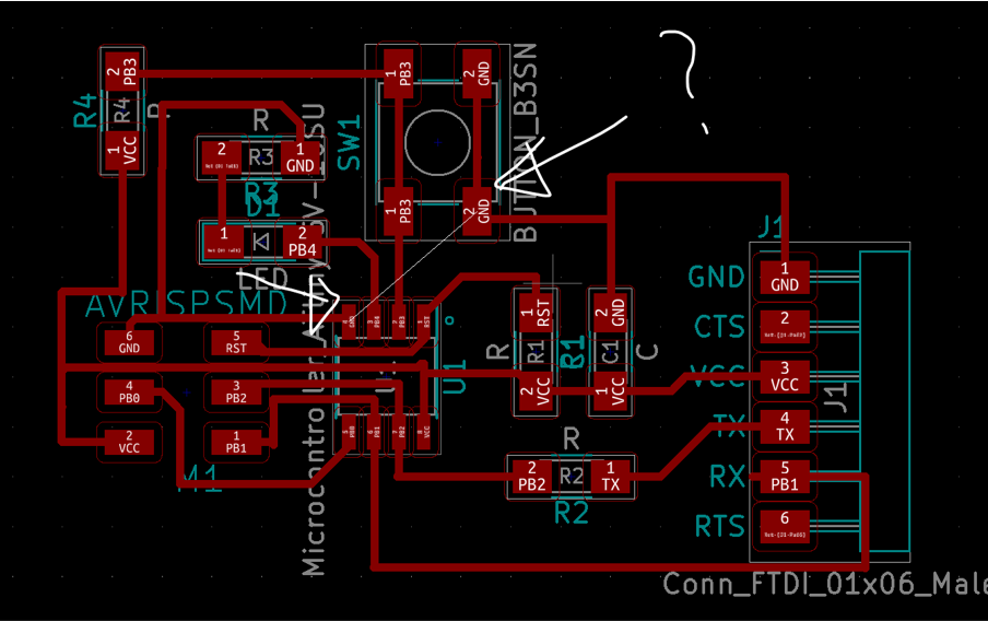
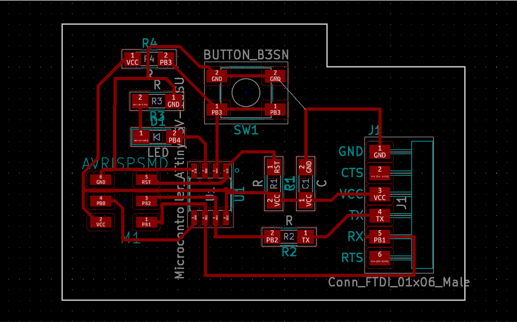
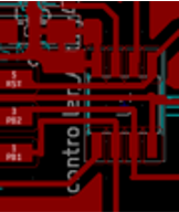
Connecting Traces
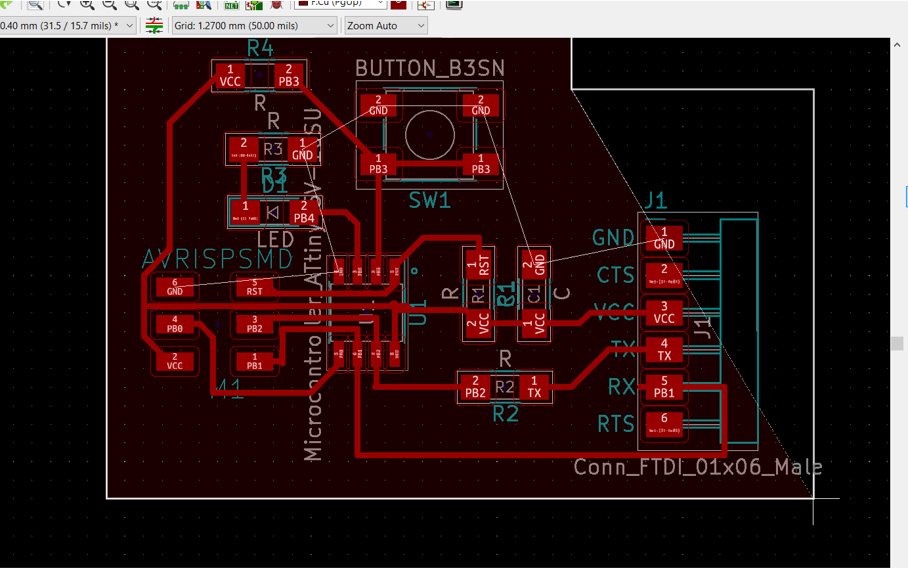
I moved the new component on top , tried to make the layout as it show in the picture on the right
After connecting the component like the one in the picture I can notice here is the place to the push button and the led
Connecting Traces Solved
every thing went smooth after connecting the main component, the last problem was connecting GND of ATtiny45 , push button , ftdi connector,
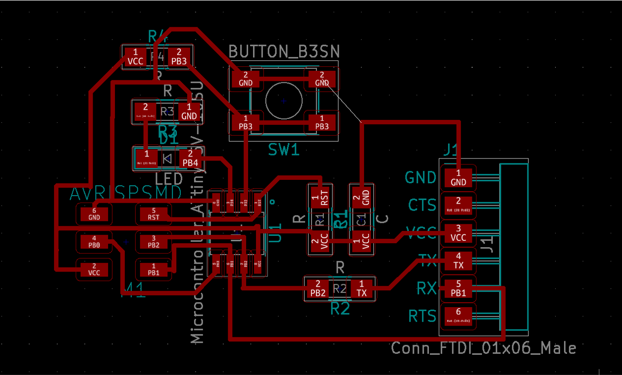
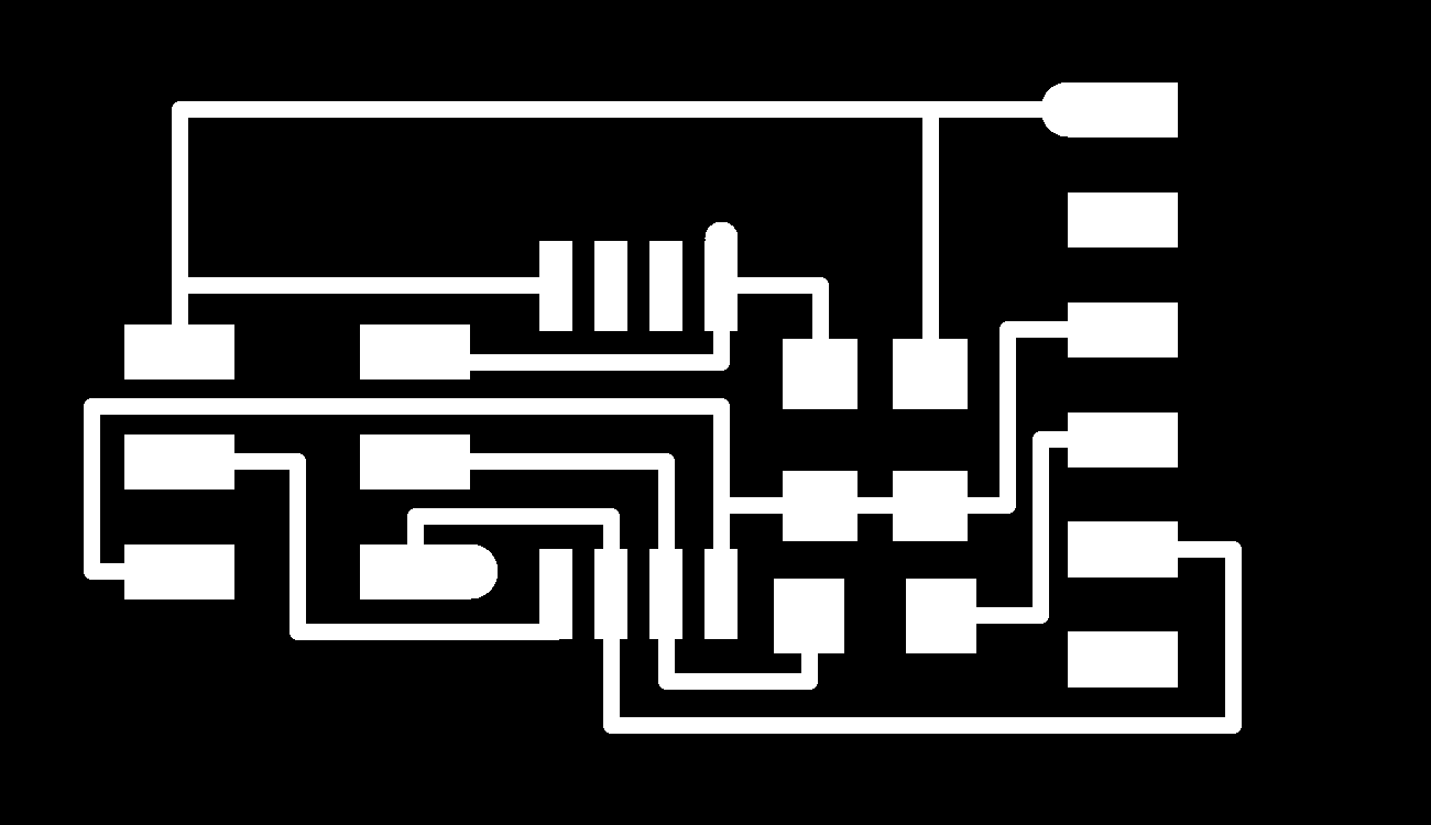
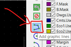
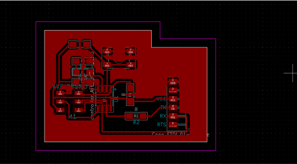
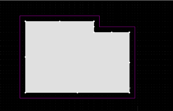
Adding Outline Boarder
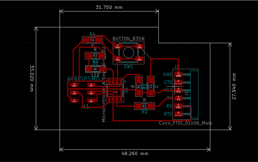
after connecting all traces now its time to make the boarders, you can use the graphic line button on right side bar , then make sure of the size of your board by measuring it with
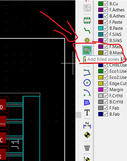
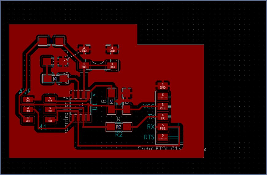
Fill and connect GND
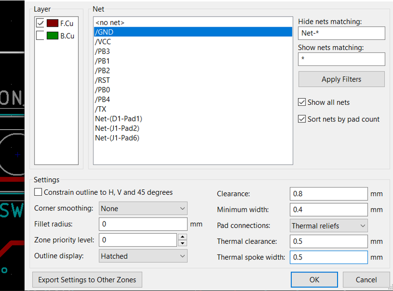
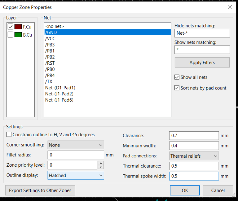
to make board cleaner you can fill the empty spaces and to make use of the filled copper to connect all GNDs together, you can do that by click add filled zone button found on the right side bar, then click on the border, a window will pop up choose Fcu and choose GND and specify the clearance and distance according to your machine and your mill bit
Fixing filling error
by testing the electric rule i can notice the problem that showing its mean there is some unconnected places and from the fill, so i solved it by reduce the clearance spaces, another problem is that the ground of ATTiny should not e connected directly to the other grounds, it should be connected to capacitor ground only , so i used the keep out area button to unconnected it from the fill and connect it ageing to the capacitor
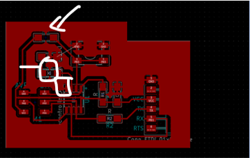
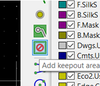
Adding Keep out Area
by click the keep out button on the right side bar, and then select the area to keep it out of the filling, and the area we want to keep it out is the area arount the Attiny45.
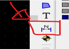
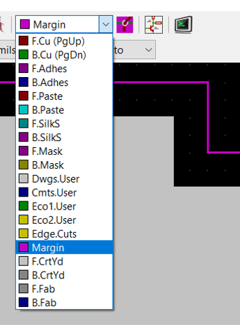
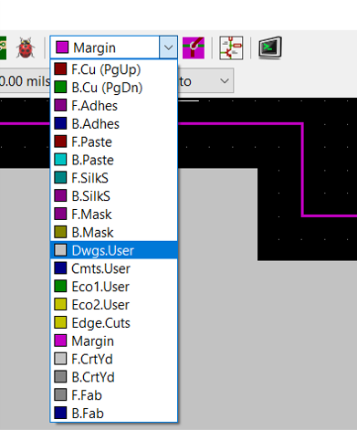
Add margin, and select your cut area
then add margin around the pcb in order make the machine cut the border, change the view to margin and use graphics lines and draw the border , next change the view to Dwg.User and draw around your drawing.
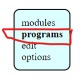
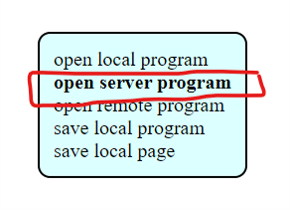
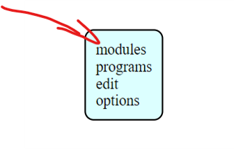
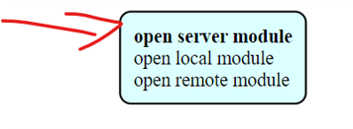
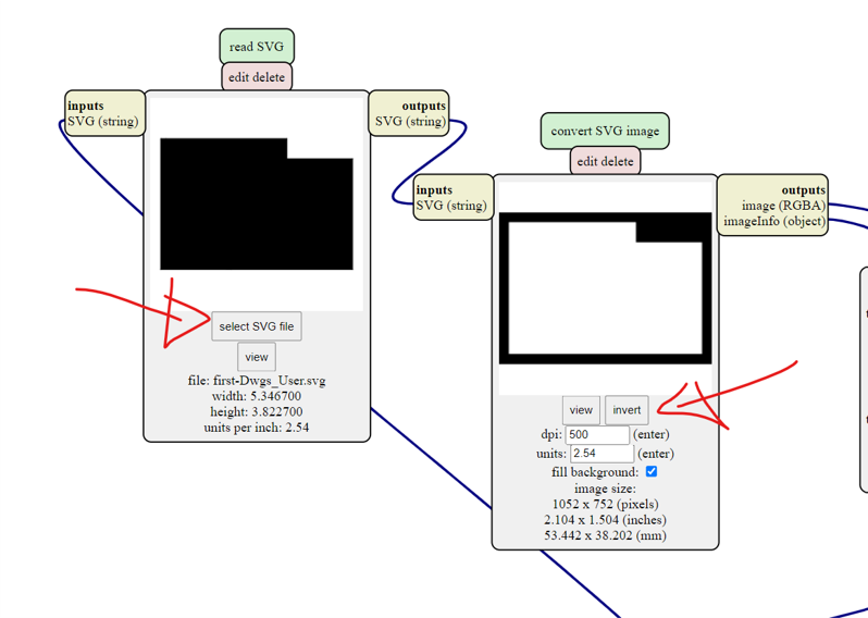
Now open mods form Here
Start by Right Clicking your muse, then choose programs , then open server programs ,then PCB Svg
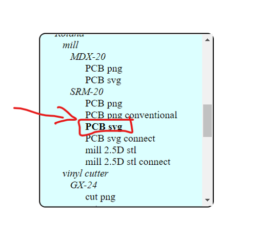
Now this is over view of the program you can find link on what dose each model Do From here
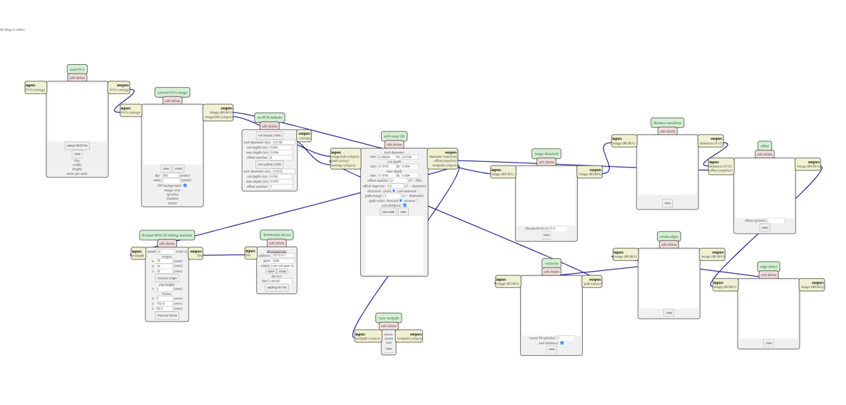
Upload picture to mods
So first select the file that want to cut, and then invert it in order for the Machin to mill it correctly, click invert to invert the black with white color
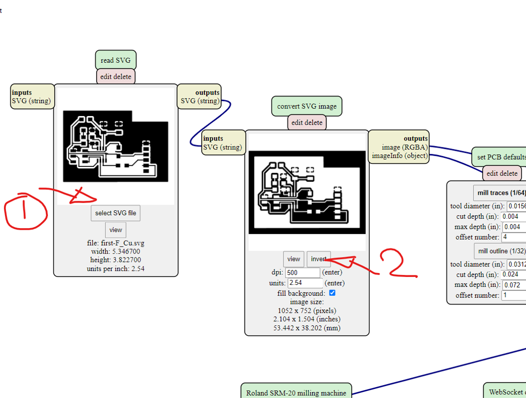
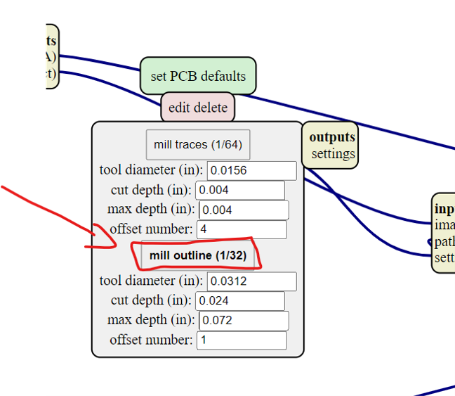
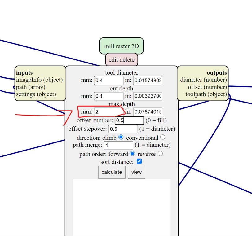
Tools diameter
now put the diameter for the cutting , make tool diameter to 0.4 mm and the drill depth to 0.1 mm and then hit calculate, make the speed 4 and the XYZ axis to zeros.
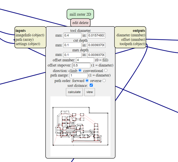
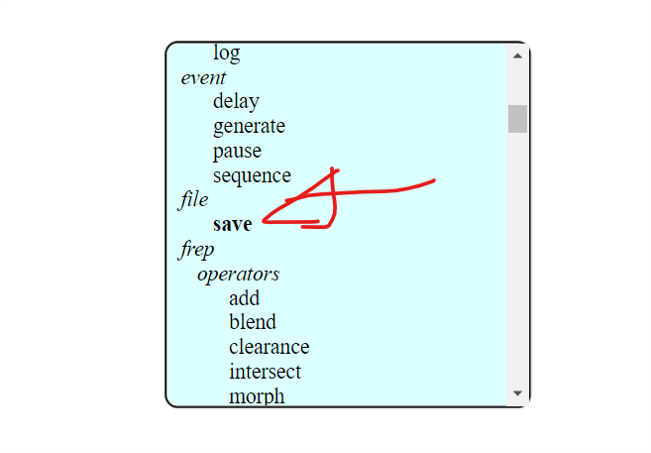
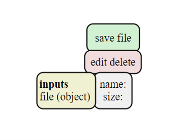
Saving and downloading the files
in order to save and download the file you have to add another module to the end, delete the WebSocket device model and replace it with Save file module
click calculate
Repeat for the margin cut file
repeat the same process for the margin cut but change the depth of the cut to 2 mm
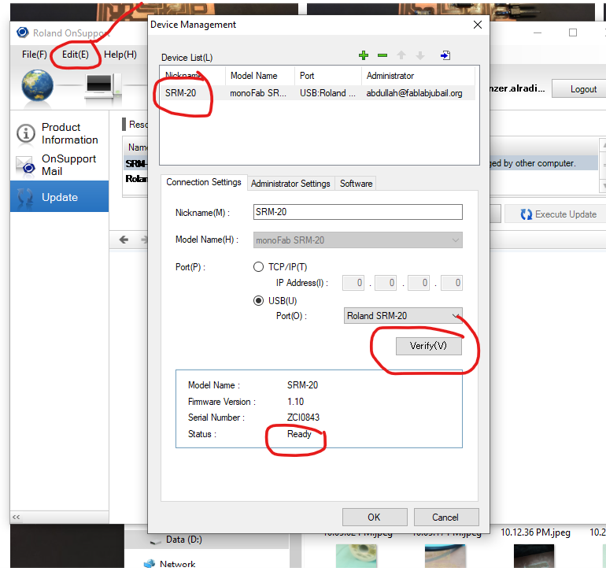
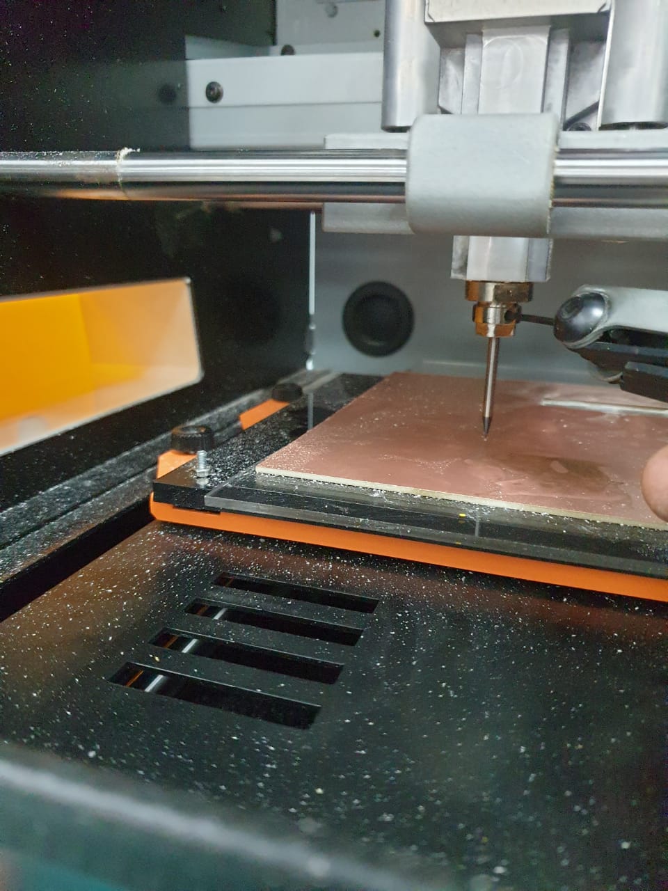
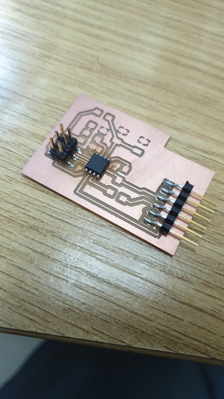
Cutting with Roland SRM-20
now its time to set the machine to cut the circuit, i have full documentation on how to use Roland srm-20 and its software VPanel Here
- open OnSupport and connect to the machine
- open VPanel set the origin and zero axix
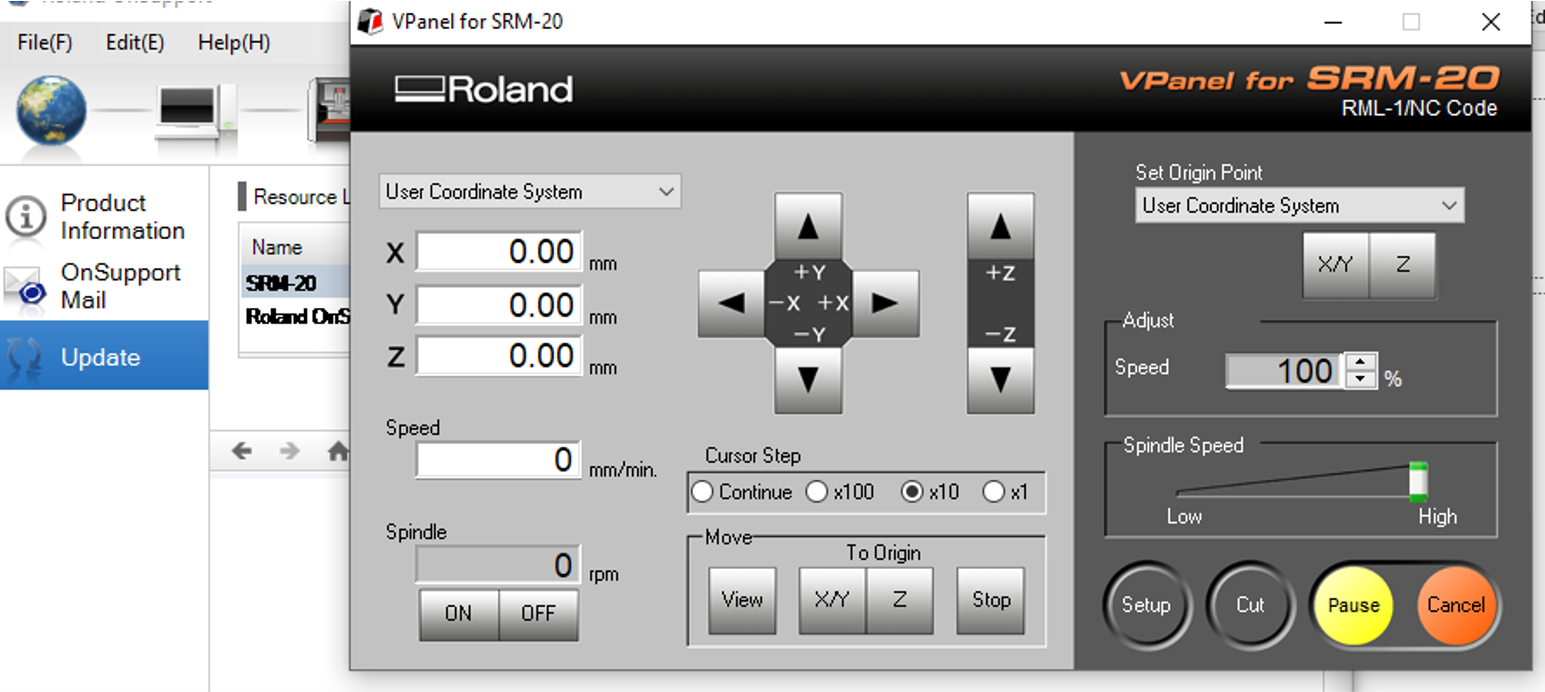
Cutting with Roland SRM-20
now its time to change the bit to 1/64 to make the z axis to zero.
i broked the bit
After removing the nail from the drill, I lowered the machine and forgot that I had put it in the continuous Mode, and broked the bit. every thing stopped here till i order another one to continue

buying new bit and continue the work
it took one week to be able to find new bit to continue with the work so i bout couple of 1/64 and 1/32 to not stop again if one is broke,
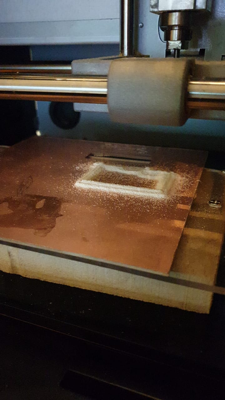
i already finished with setting the mods for engraving the circuit so i did that first then i changed the setting to cut it out.
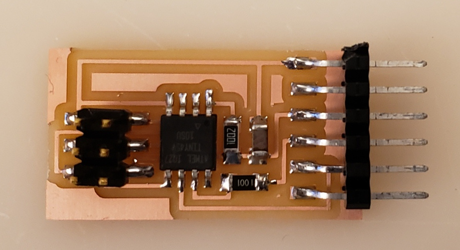
soldering the circuit
After cutting the circuit now its time to solder the electronics parts and pins on it, i use glue to fix the parts on the circuit first then used solder ink and heat gun to solder it
programming ATtiny45 With Arduino as isp
first you need to have Arduino ide you can download it from here depends on your operation system choose the one suitable with you
programming ATtiny45 With Arduino as isp
i foloowed this toturial to upload the sketch using
add attiny board
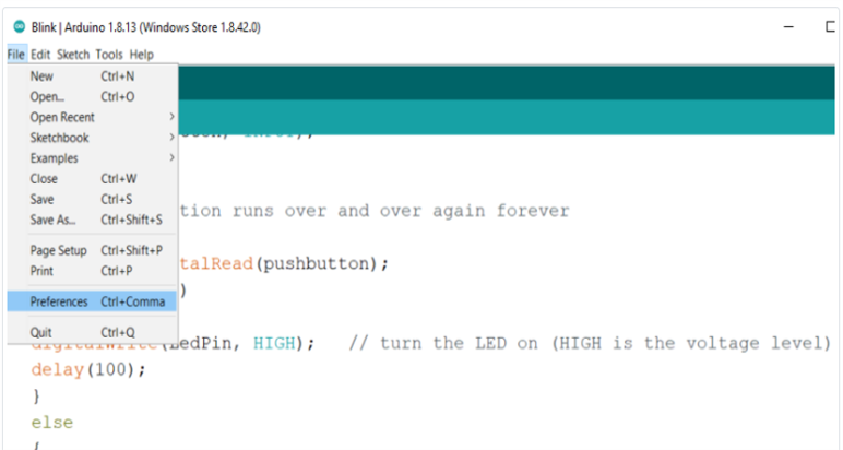
First you want to open File > Preferences.
Then, at the bottom of the pop up menu where you see “Additional Boards Manager URLs” you want to copy and paste “https://raw.githubusercontent.com/damellis/attiny/ide-1.6.x-boards-manager/package_damellis_attiny_index.json" (without the quotation marks).
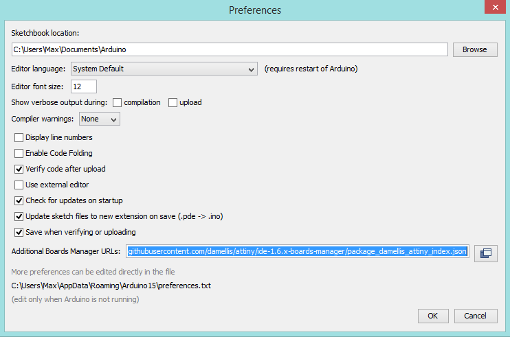
Now click OK.
Navigate to Tools > Board > Board Manager.
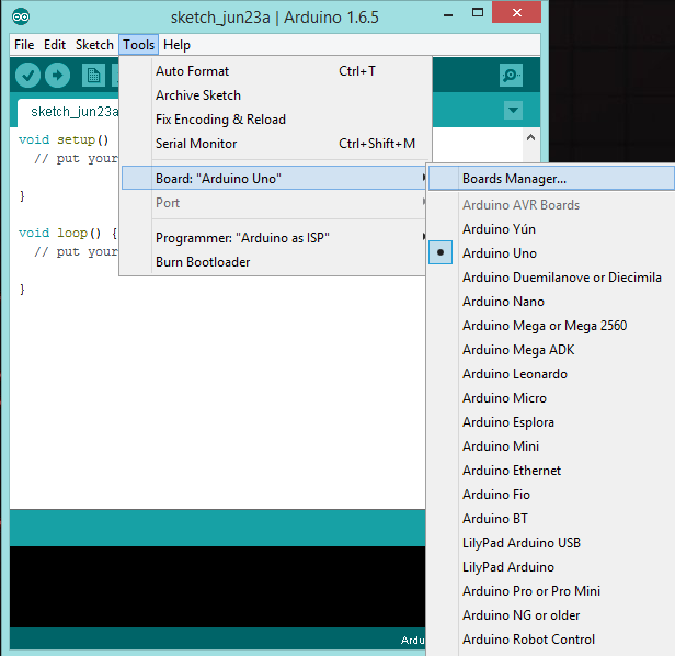
Scroll down to the bottom and you should find “attiny”. Click the install button and the words “Installed” should appear when the task is complete.
To confirm that you have added support for the boards, navigate to Tools > Board and you should see ATtiny at the bottom of the list.
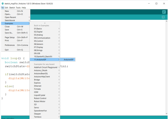
Setup Arduino As ISP
Navigate to File > Examples > ArduinoISP. Open the sketch and upload it to your Arduino.
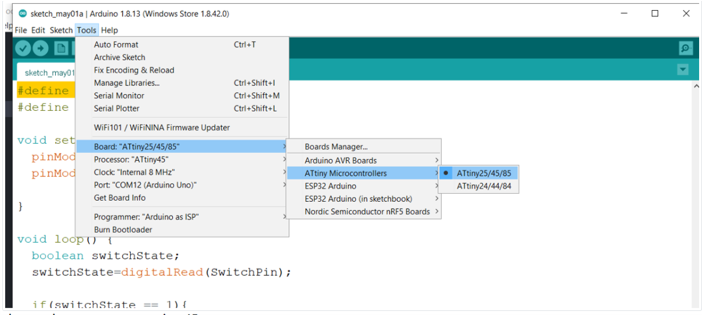
choose the board attiny microcontrollers attiny 25/45/85
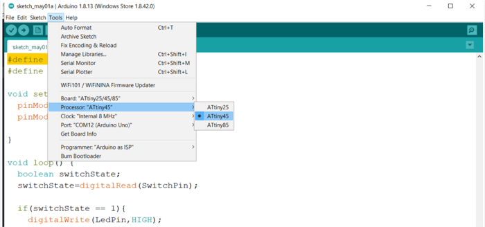
choose the processor to attiny 45
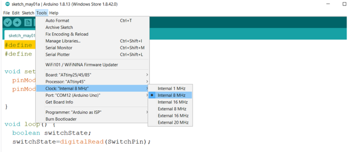
choose the internal clock 8 MHZ
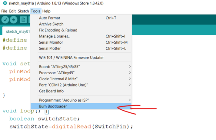
burn bootloader
pinout
testing with blink example
adding button to the code
Arduino program
you can download Ardino program from here
Kicad Files
you can download Kicad files from here you can download SVG files from here