Assignment 4
Fabrication of an ISP
Furthermore we were asked as a group task to evaluate our milling machine concerning 'PCB Production Specifications'. I.e. how it mills under certain parameters. Have a look at the group project page to see what we have done.
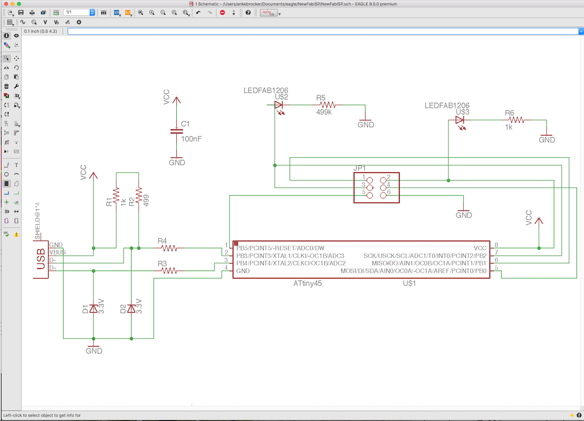
Schematic and Board Design
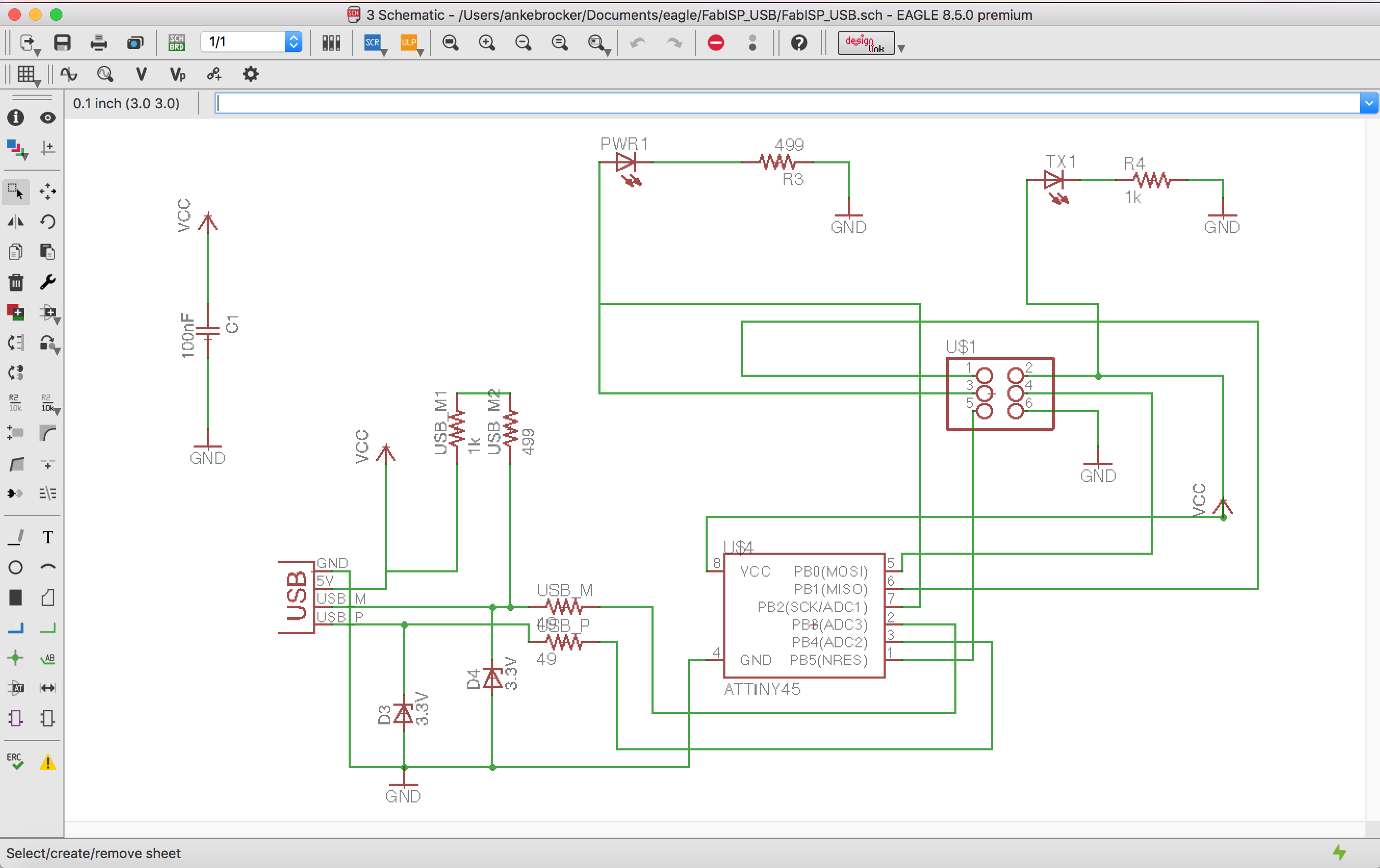
1. The most challenging part during the design was finding the correct digital components that represent the desired components on the real world. Eagle is presumably a good software for experienced users. But as a novice learning how to handle the software is hard. The tutorial
mentioned before and also asking our local instructor helped me. Furthermore, the archive of the FabAcademy. When creating the schematic each
component has a little cross, which can be seen as the handle to control/move/edit (move/rotate tool etc. need to be chosen before and can be found on the left of the application) the component.
2. I decided to not include the jumper, that Brian has. As I do always want my ISP to be powered when it is used. Apart from that I built my schematic like he did on his website.
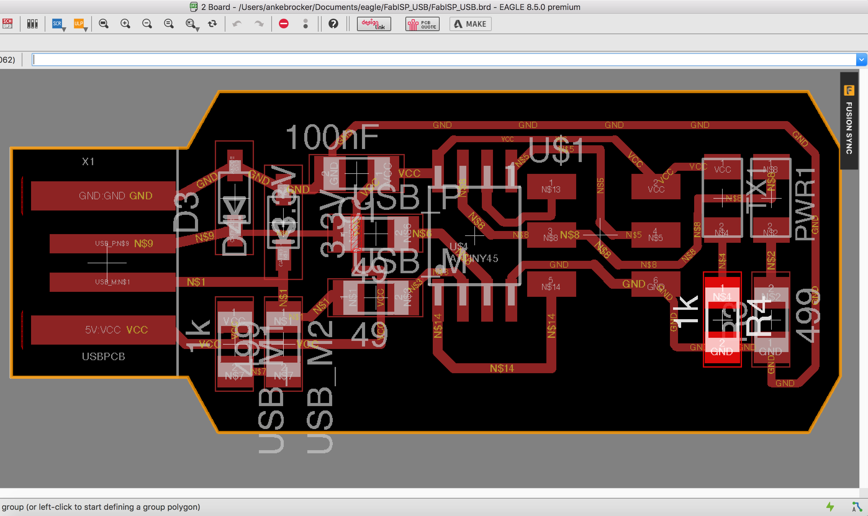
4. After designing the schematic I started designing the board of my schematic. To start I pressed
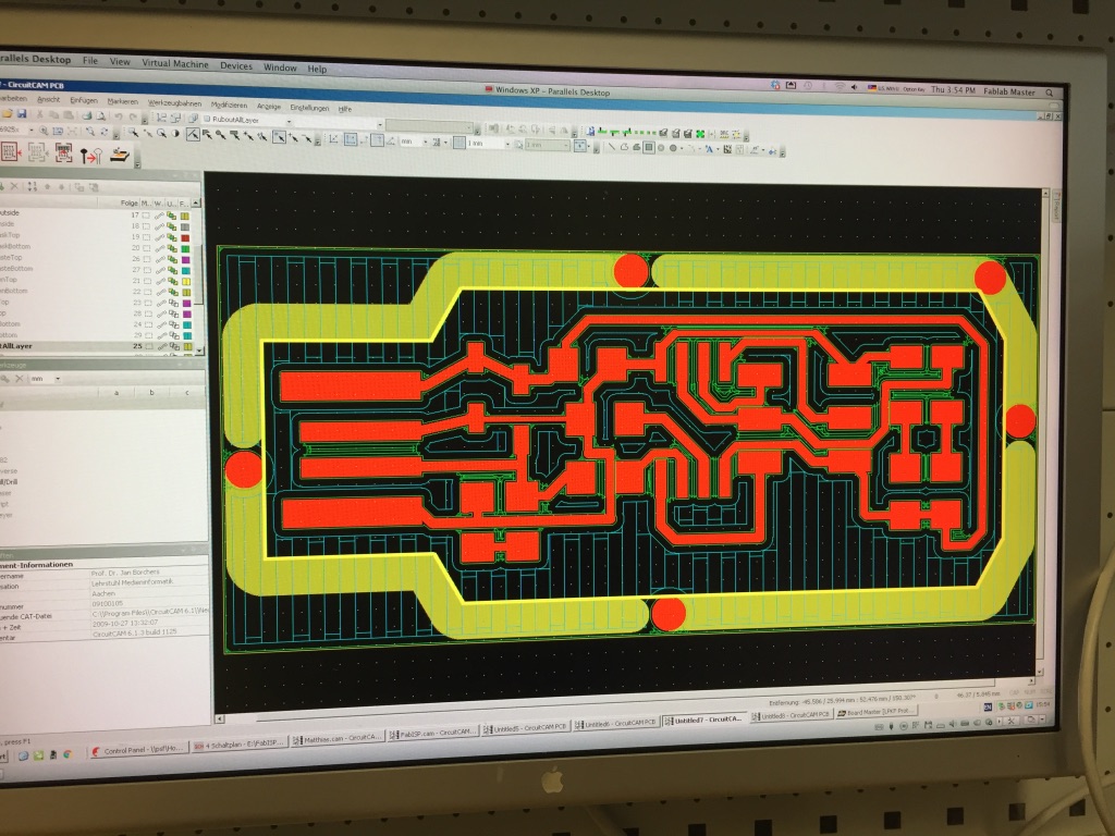
As Brian does include a picture of the board layout I took this picture as an orientation while routing. This way it was a lot easier. All in all, it took about 30 minutes to route all connections manually. You can find the schematic and board files at the end of the page.
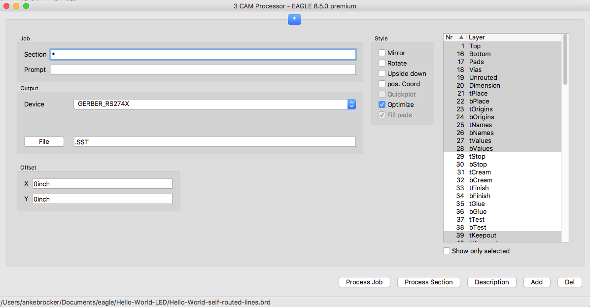
Cam Processor Eagle
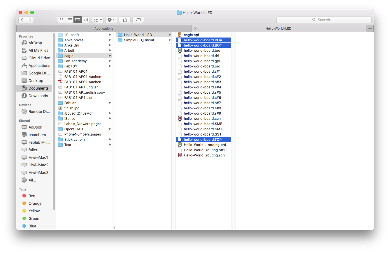
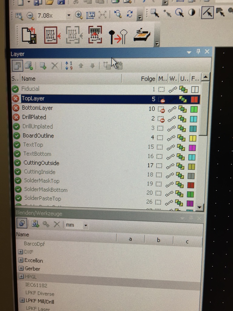
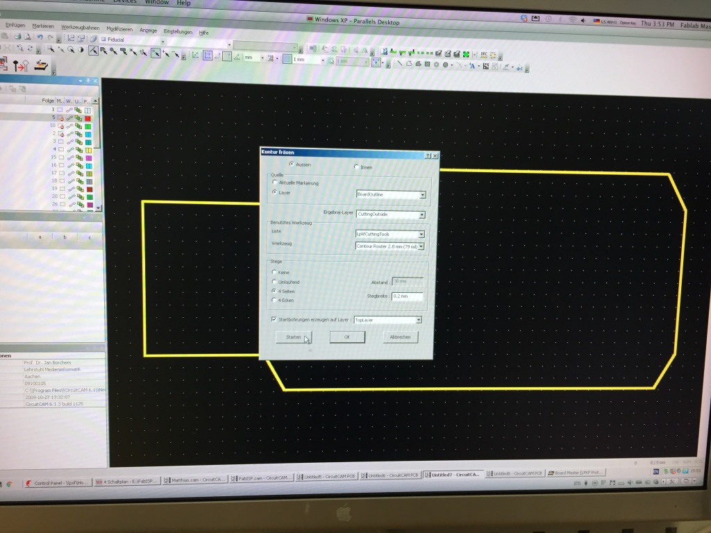
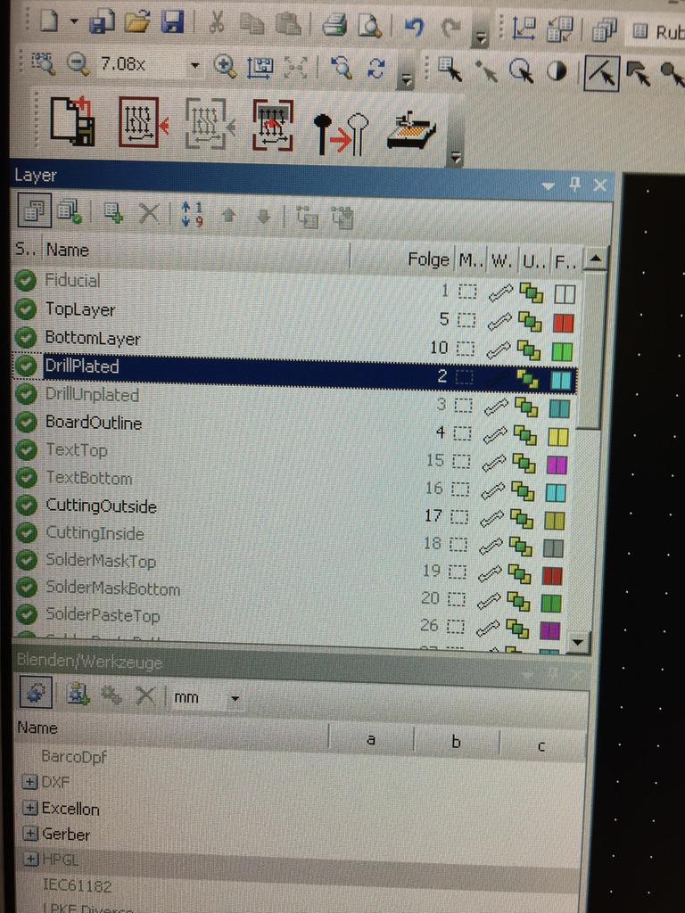
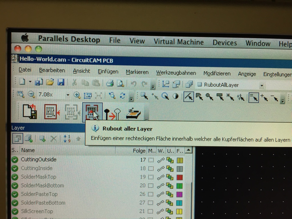
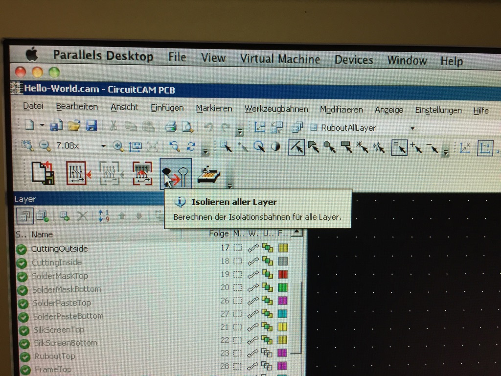
As the board design was finished the board needs to be prepared for the milling. Therefore, four different files need to be produced, which are .BOT, .DRD, .TOP, .BOA by clicking the ![]() button.
button.
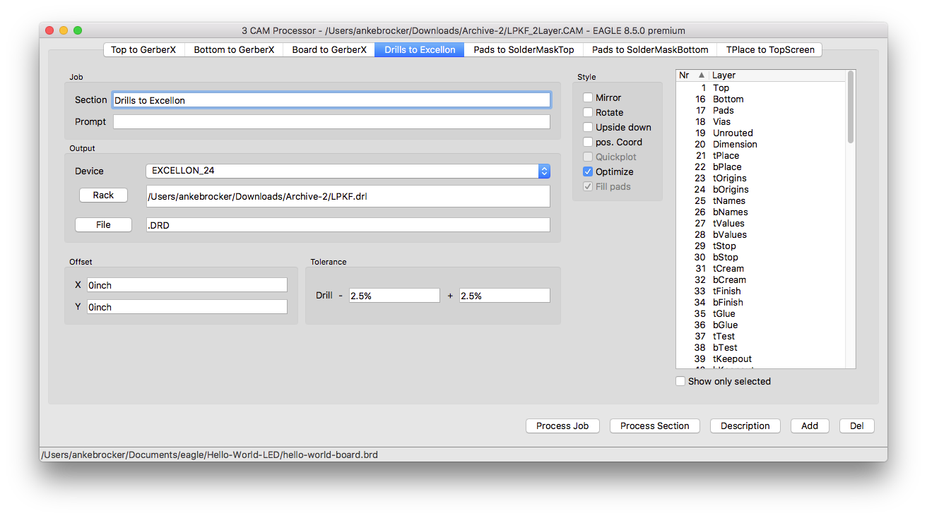
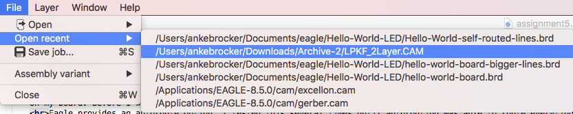
If you are not able to choose the tab 'Drills to EXCELLON' you need to choose 'File < Open recent < LPKF_2Layer.CAM'. After this follow again the steps of above pictures a. and b.
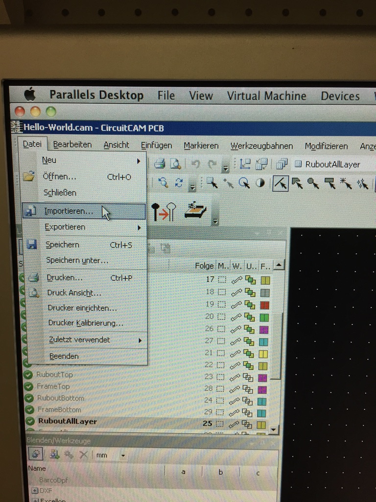
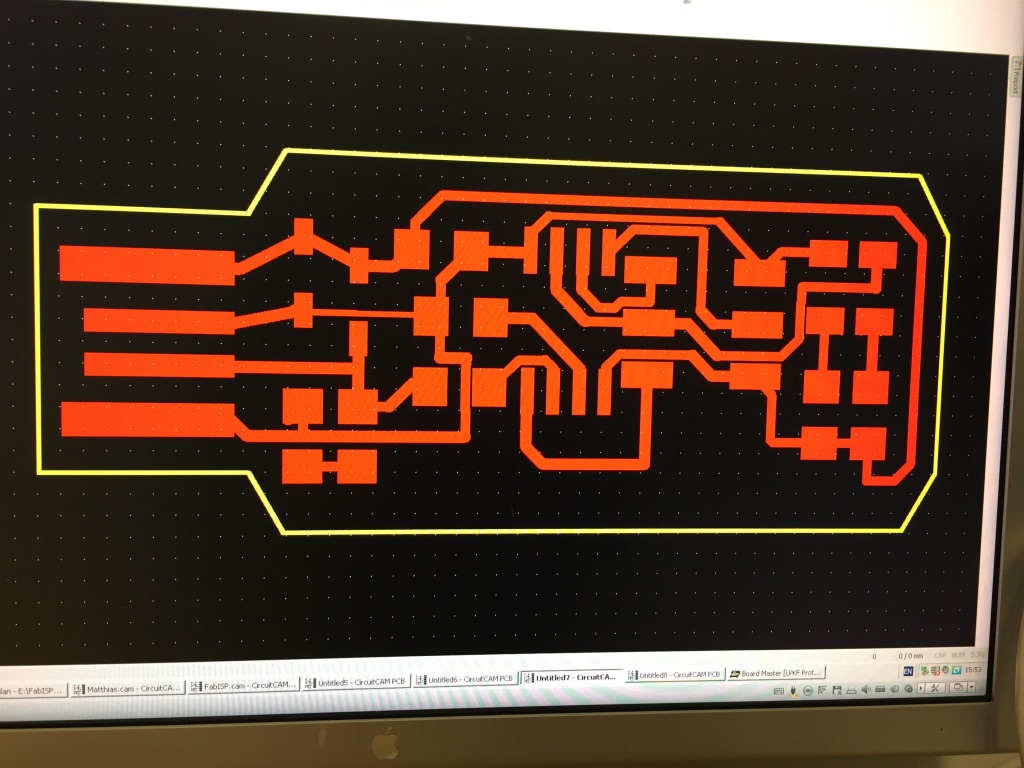
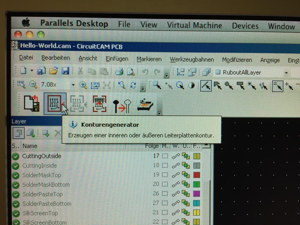
CircuitCAM Software
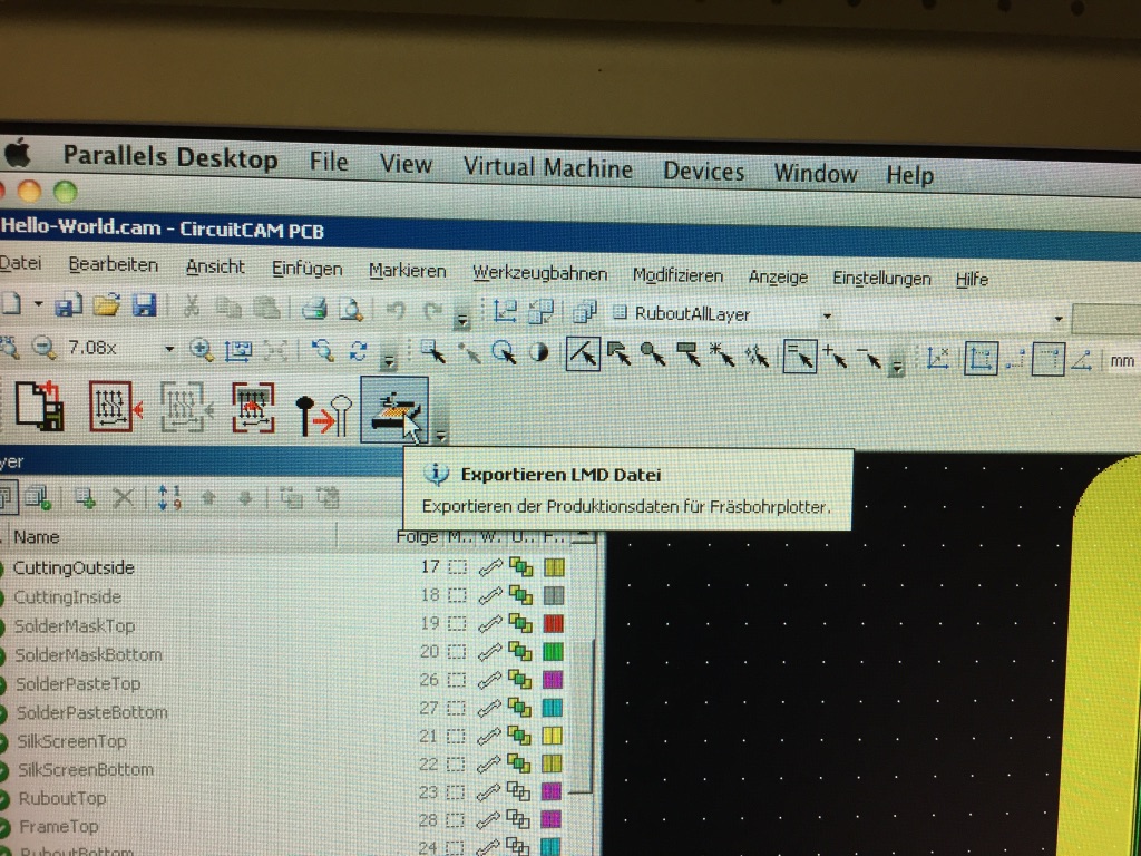
Before the board can be milled it needs to be transferred into a LMF file which can be opened by the boardmaster software used by the milling machine.
Board Master Software & Milling
In our FabLab we have a LPFK milling machine. With the software boardmaster you can control the milling machine. Important advices to mill your PCB and to assure a connection between the mill and the software and a proper working mill process:1. Turn on the milling machine first, otherwise the software cannot connect to the machine.
2. Do not open the milling machine while it is milling your PCB!
3. If the machine stops working or looses connection without any obvious reason the easiest way handling this is: Closing down the software, turn off the machine, turn on the machine and open the software again.
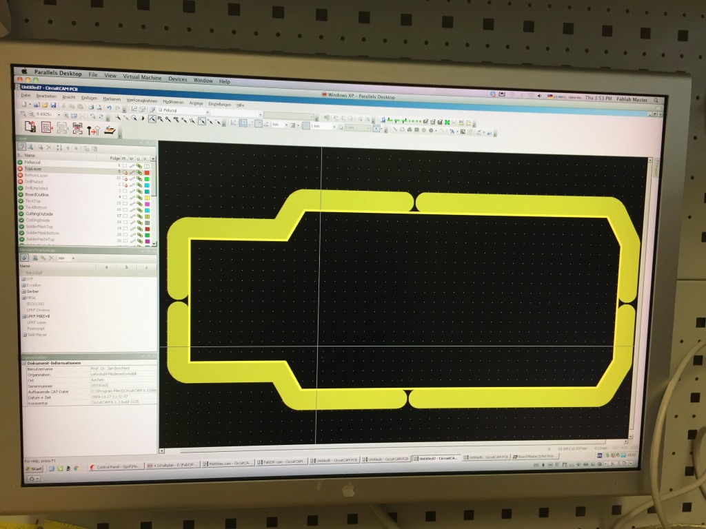
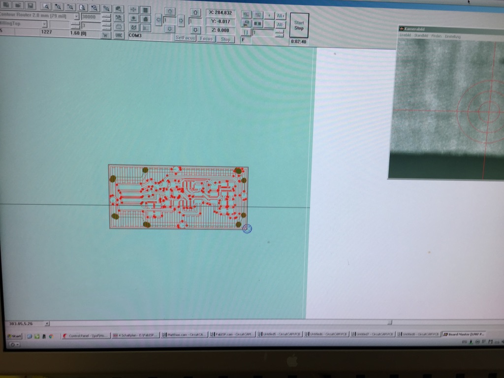
Following you see the steps to prepare the LMD file in boardmaster to mill it:
1. When clicking the symbol to export an LMD file in CircuitCAM the file was sent directly to the boardmaster software.
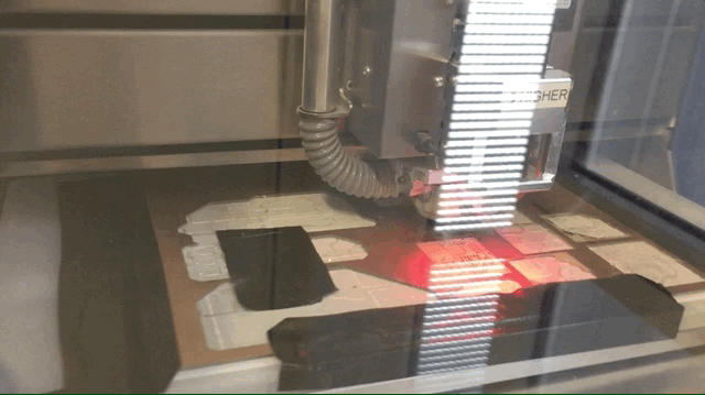
2. Now you need to move the milling head into the correct position. As a hint, mark your PCB in the mill with a dot where you want to mill your PCB. Look for this dot with the camera of the mill machine head by moving it with these
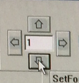 arrows in the boardmaster. You can define the step size with the number in the middle of the arrows.
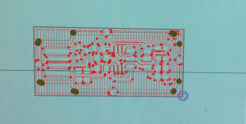
3. Now move the mill head to the camera head by clicking 'Verfahre nach < Kopf>>Kamera'. Afterwards, also move the digital board with the tool ![]() in the boardmaster software to the blue circle, which indicates the mill head
in the boardmaster software to the blue circle, which indicates the mill head
 .
.
4. You need to execute three parts to complete your PCB: Drilling plate, Milling Top, Cutting Outside. Those need to be executed separate and after each other. You can choose the parts here
![]() .
.
5. Every time before you start milling one part you need to click 'All+' and then 'Start' 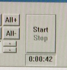 . Follow this instruction for each part and mill your PCB.
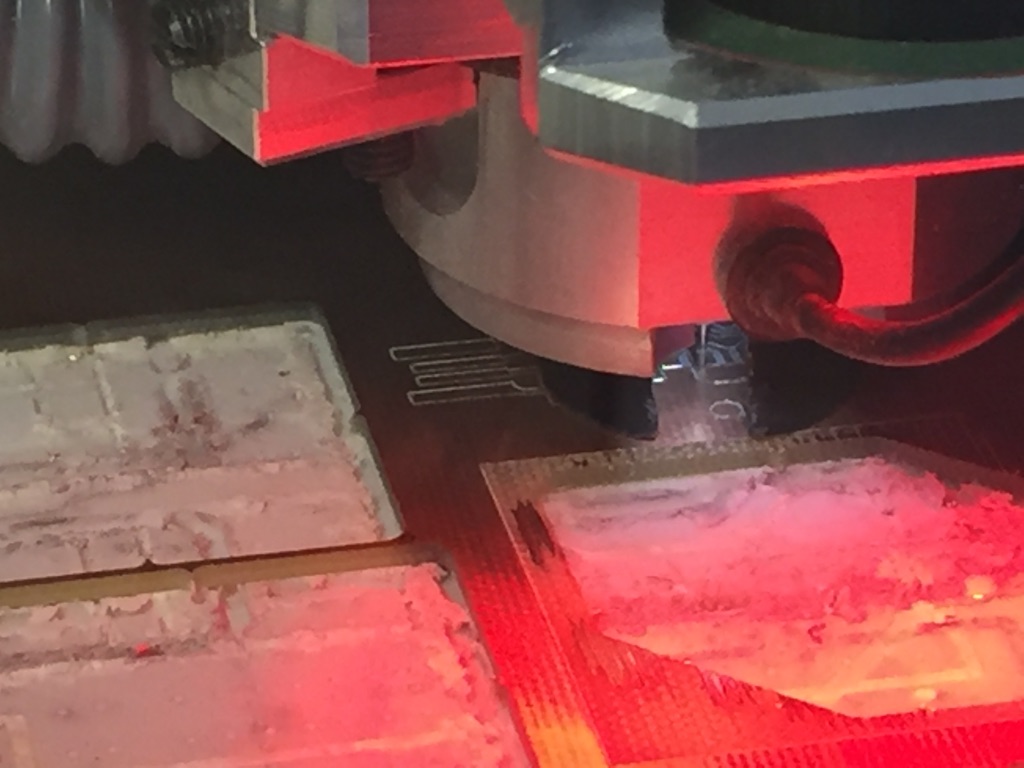
6. After executing all milling dissolve your PCB from the shield.
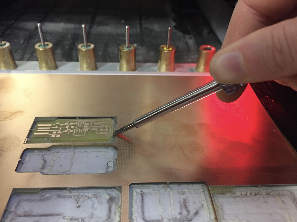
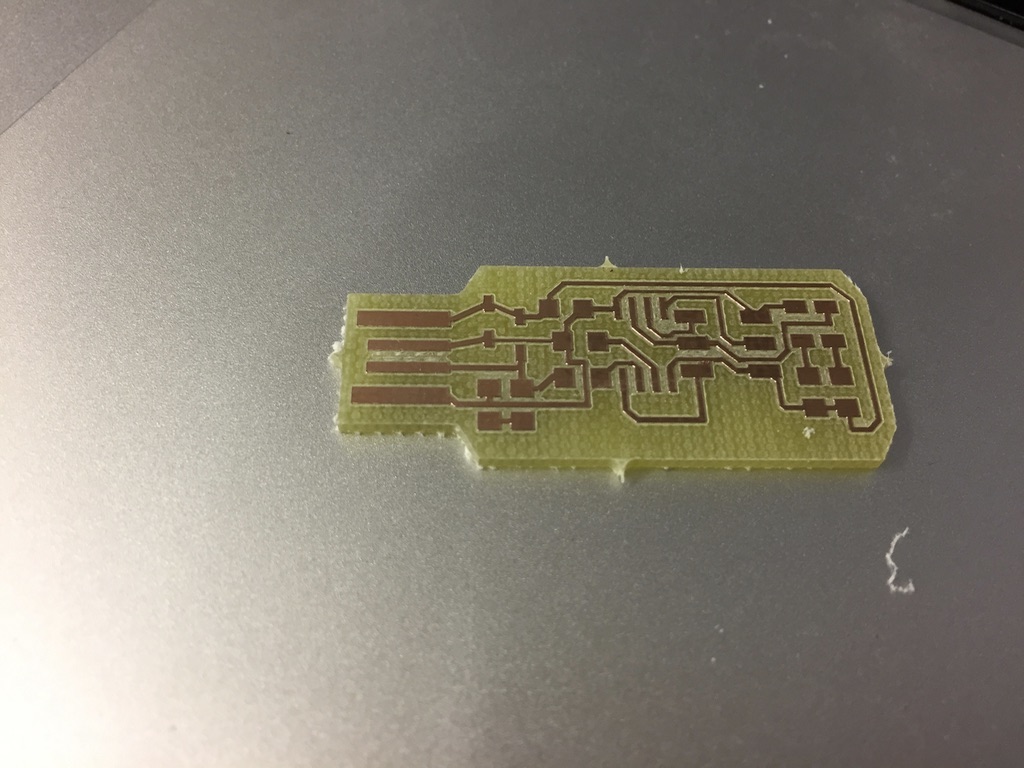
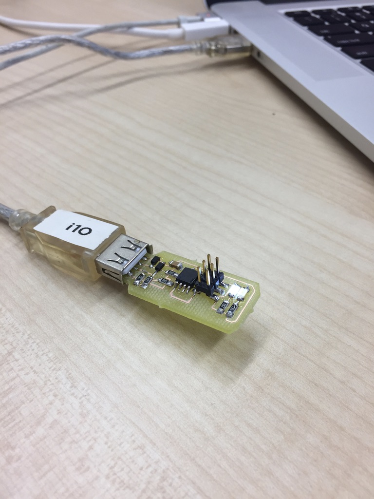
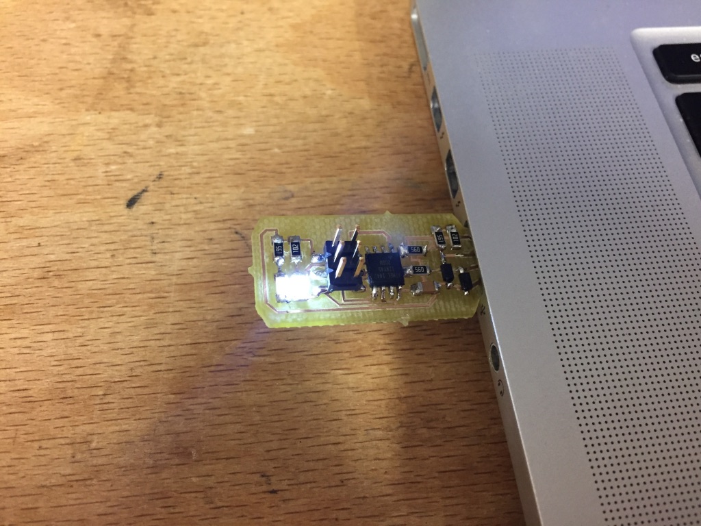
Soldering
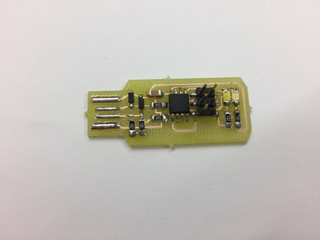
As mentioned before soldering was the only part of electronic design I had experience in. First, I collected all the needed components from the FabLab drawers:
1 x Attiny 45
1 x 100nF SMD Capacitor
2 x 1kΩ SMD Resistor
2 x 560Ω SMD Resistor (Brian used 499Ω)
2 x 56Ω SMD Resistor (Brian used 49Ω)
1 x red SMD LED
1 x green SMD LED
2x 3.3v zener diodes
2 x 3 SMD Pinheader
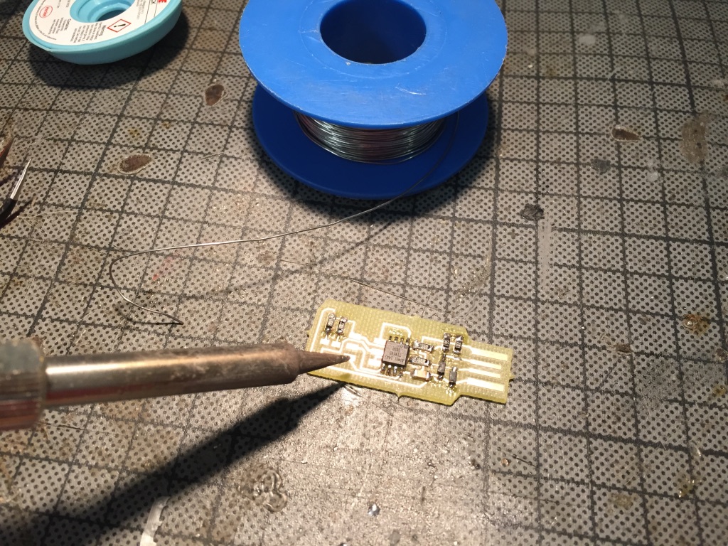
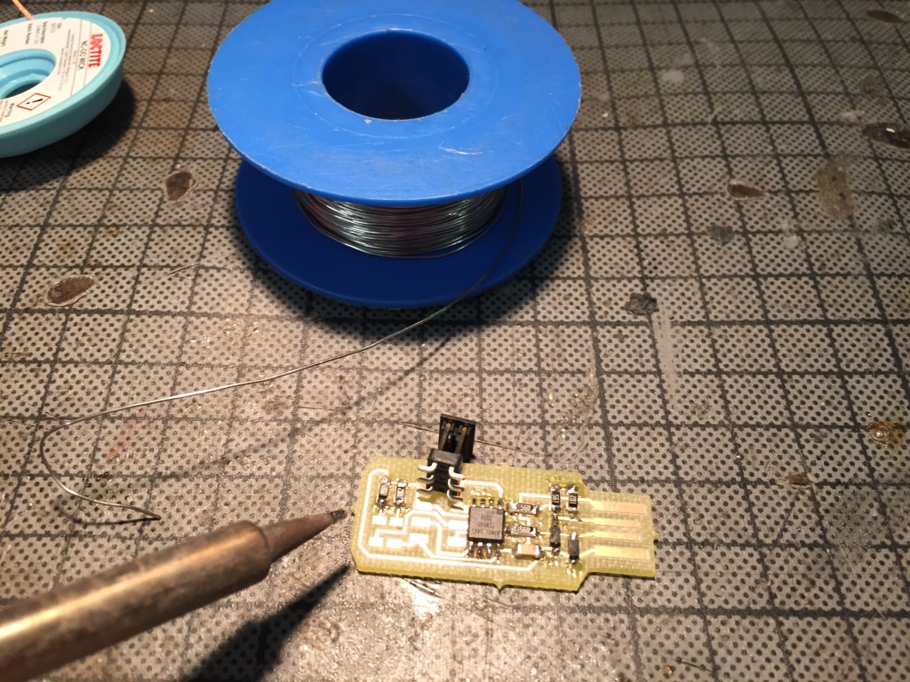
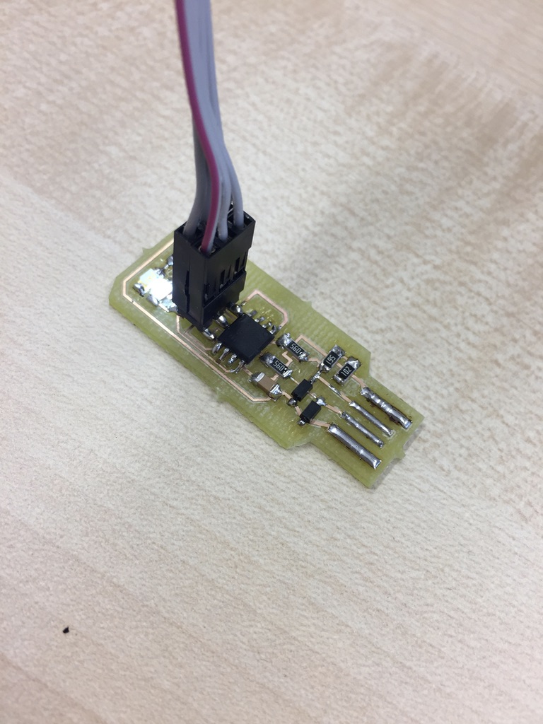
Then I started soldering. At first, I soldered the ATTiny and afterwards all the other SMD parts to have an even surface to solder on. At last I soldered the 2 x 3 pinheader as it is quite high and could be in the way while soldering.
During soldering I used a multimeter to assure regularly that I did not solder 'short cuts'. The very last step was putting solder material onto the USB contact points that should connect to a USB
port.
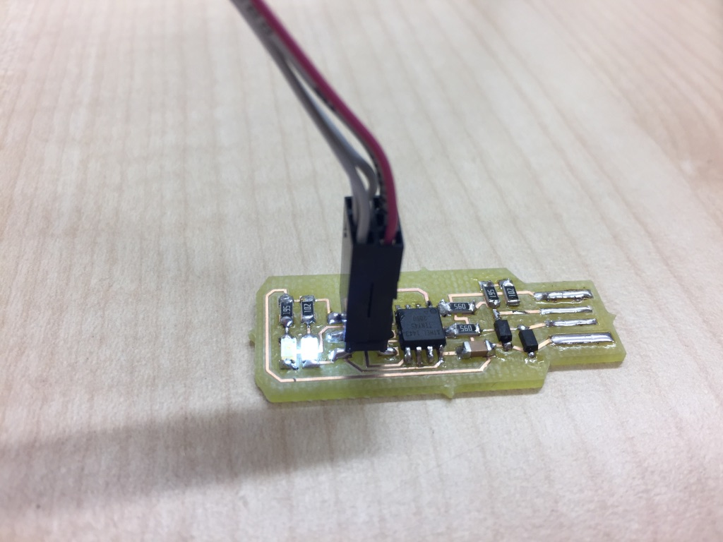
Programm the board as an ISP
For me programming was the most challenging part during this assignment. I did do programming an Arduino before but that was with the ArduinoIDE. Getting to know
how to flash a device in a terminal was e.g. one aspect that I had to look up. Again, the website of this student helped me
finding out. To program the board as an ISP I followed Brian's steps. Thanks to Matthias
who gave me some steps I should follow to assure all drivers etc. are installed on my computer as some steps are not clear stated on Brian's website. Even with this helped I did destroy
one ATTiny45 (shame on me).
As Brian did miss detailed steps I will list all the detailed steps before your are able to program the board:
1. Install Crosspack2. As I had not installed brew yet, I had to do this (from the terminal run: /usr/bin/ruby -e "$(curl -fsSL https://raw.githubusercontent.com/Homebrew/install/master/install)")
3. With the help of brew I installed libusb (in the terminal: brew install libusb-compat)
4. Download avrdude (version 6.3) from here. Unpack the downloaded archive. Navigate to the unpacked folder in your terminal and run './configure'.
Assure the output tells you: DO HAVE libusb right at the end (Configuration summary).
Afterwards run 'make' and after that run 'make install'.
5. Download the drivers from here and install them.
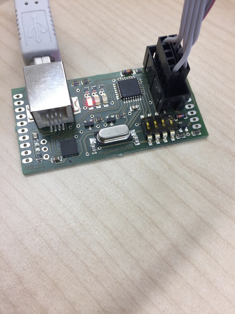
6. Connect the mySmartUSB MK2 to the laptop and then the FabISP to the mySmartUSB MK2 to program it as an ISP. Assure to connect ground to ground Pin etc.
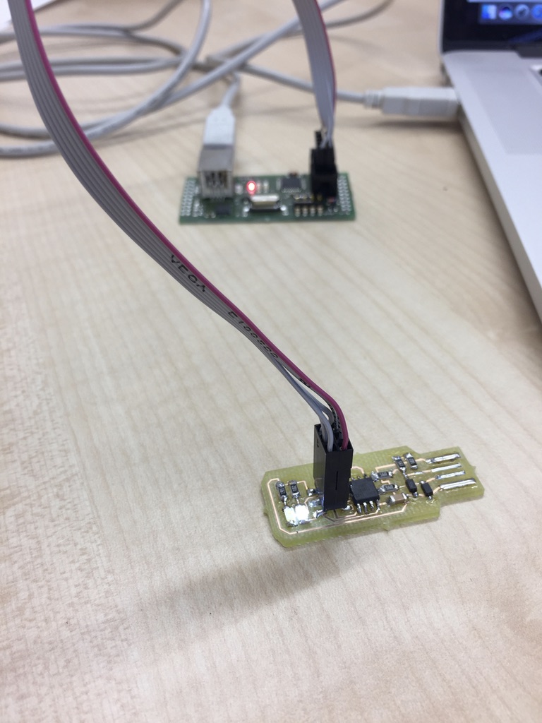
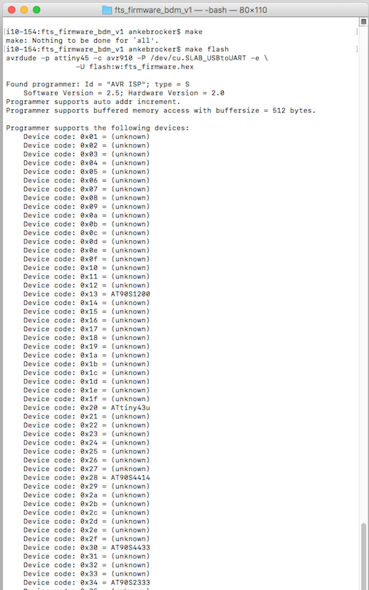
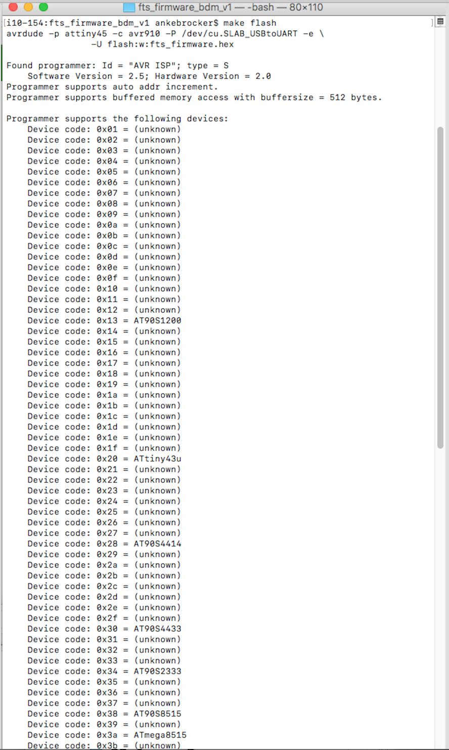
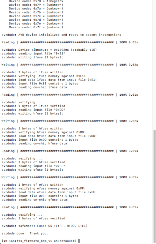
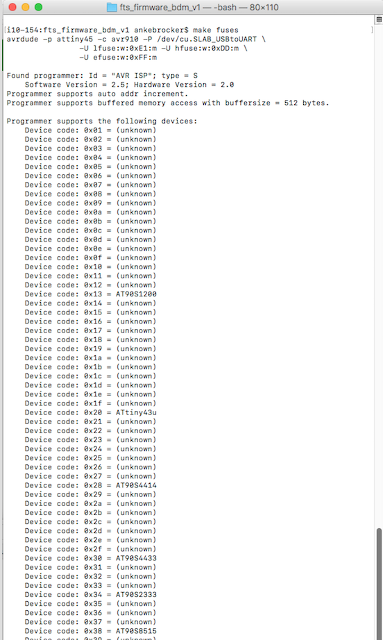
7. Now I ran the following commands, which can be seen in the terminal output pictures below:
* make
* make flash
* make fuses
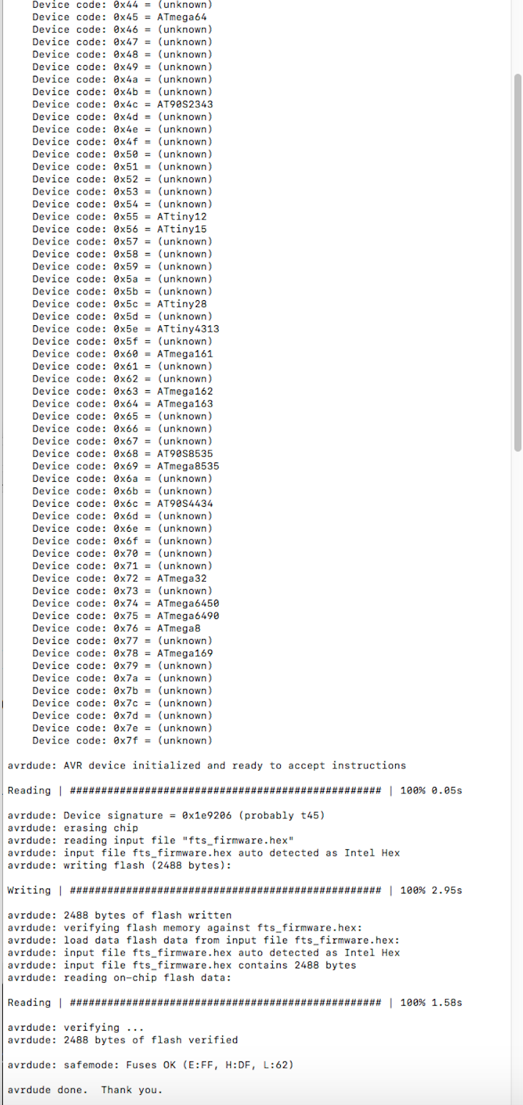
8. Afterwards I checked if my FabISP was now recognised as a USB device by my computer. For safety reasons I used an USB cable, where I connected my FabISP. I checked
under 'Apple symbol > About This Mac > System Report > Hardware > USB' if the device is shown.
9. As my FabISP was recognised I ran a final command in the terminal: make rstdisbl. Wuhu, now I have an own manufactured ISP =).