Week 7 : Electronics design
Eagle

Download data
Eagle
Image
Resources
Electronis design tools
Kicad (open source)
Eagle (Autodesk license)
Tutorials
Introduction to Eagle (Fabacademy tutorial)
Tamiya-san archive : Electronics design
Tamiya-san archive : Programming
Mentioned in Lecture
Drawing PCB by hand
Assignment
Hands on circuit design Prep
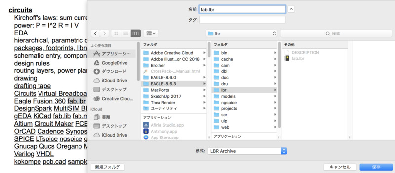
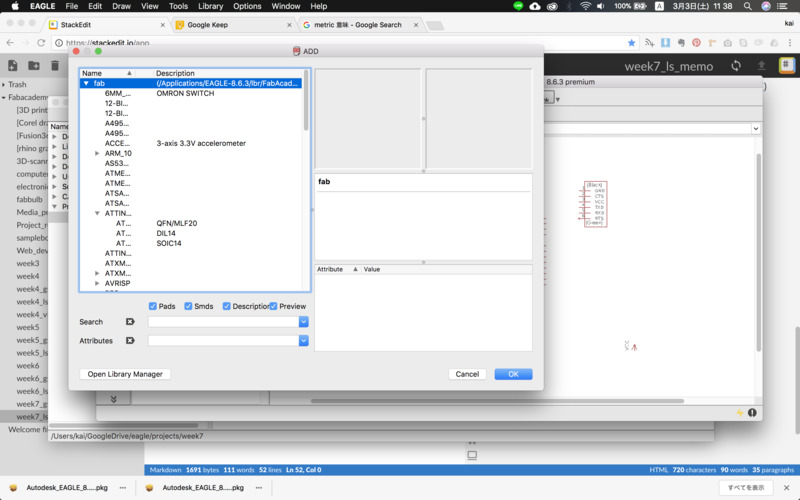
Install libraries
Download Library from Fabacademy page (Fabacademy week7)
- fab.lbr
- fab.lib : library for Kicad
- HelloKamakura.lbr : Tamiya-san’s recommnedation
Place your library file in Apps > EAGLE-8.6.3 > lbr.
note
When buying SMD chip, be careful for chip size!
Size / Dimension : 0.122" L x 0.063" W (3.10mm x 1.60mm)
- in metric : 3216
- in inch : 1206
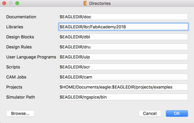
Set paths
Option > directory
Set path for “Library” and “Projects” if you want.
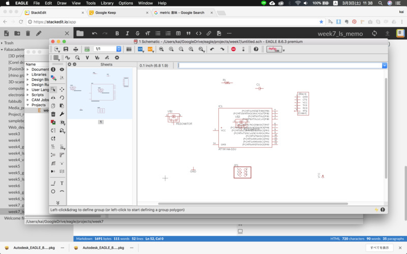
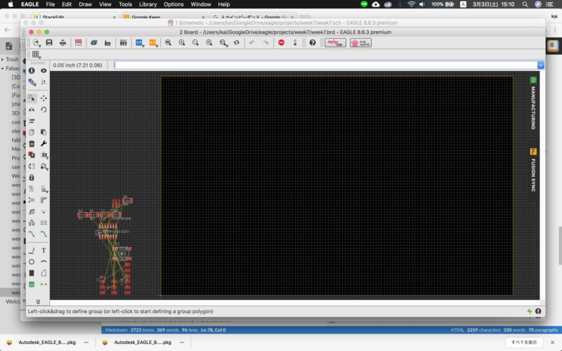
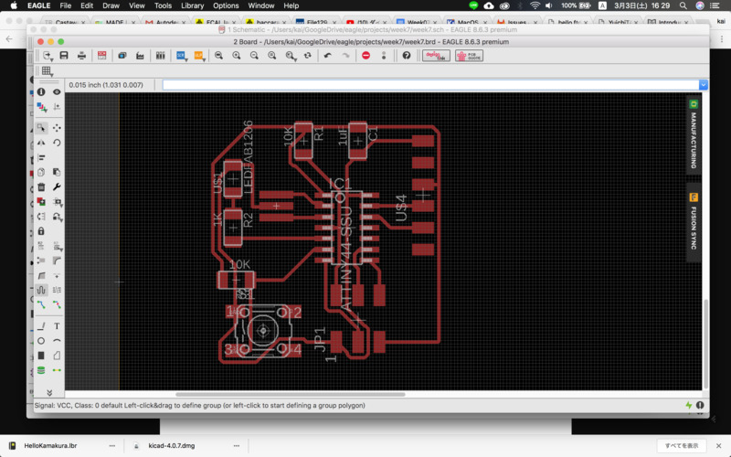
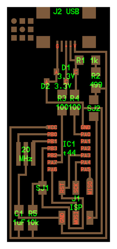
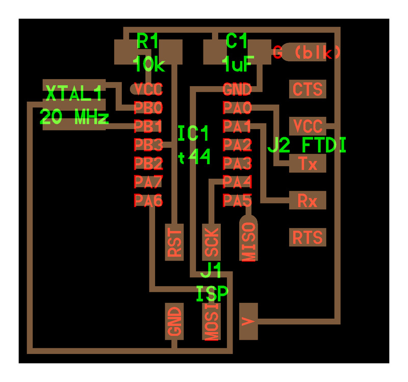
Designing circuit on Eagle
Placing and wiring components on schematic
Make new project (File > New > Project), then
Refer to board design diagram in Fabacademy week7 page
- Add components
useaddcommand.
select the components from the library, place it, then hitEsc.
- Draw wire from the components
usenetcommand and click pin on the component to draw wires.
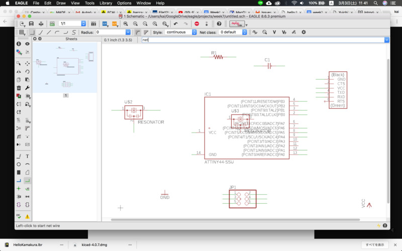
- Connect the components by naming wire
usenamecommand to declare which wire connect each other.
Click wire and name it. - Label wire to visualize what it is named.
uselabelcommand and click the wire you named.
- Insert value
usevaluecommand to insert value to component - Run Electrical Rule Check
useerccommand to run check.
Solve errors and warnings. You may ignore warning.
- When you want to rename wire, you may apply change to all wires by check “every segment on this sheet” option in name command window.
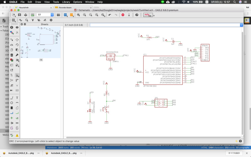
- Add VCC and GND component and connect them to other components (connecting directly from
addoverwrite the name of your wire) - You may simply connect the components by
netcommand. junctioncommand will make conjunctions at wires.movecommand let you move components.rotatecommand let you rotate components.
Design
- hit generate / switch to board
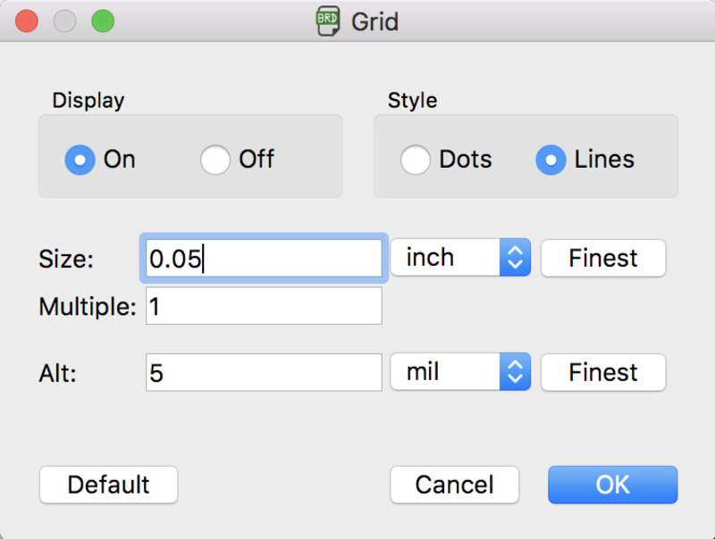
- show grid in 0.05 inch in grid dialog which could be accessed from the button in upper left corner.
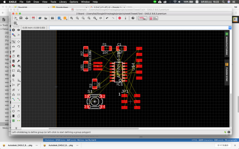
- put components in order
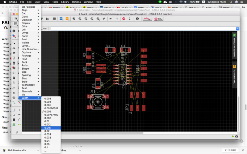
- From
changefunction, change “width” to 0.016.
- Run
ratsnestcommand to simplify airwires. - Use
routecommand to draw pattern,ripupcommand to delete pattern. Right click
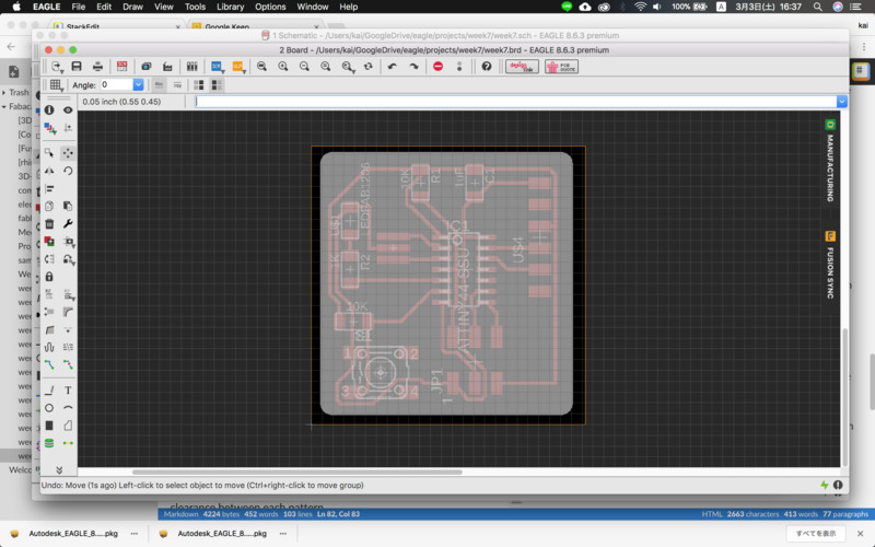
- Push layer button in the menu, select layer48, draw outline of the circuit board with
Polygon, then move and scale flame to fit the outline.
- Push layer button in the menu, select top layer (trace) and go to
File > Export > Image
Selecet PNG / monochrome / 800dpi and export.
Do the same for the document layer (outline) too.
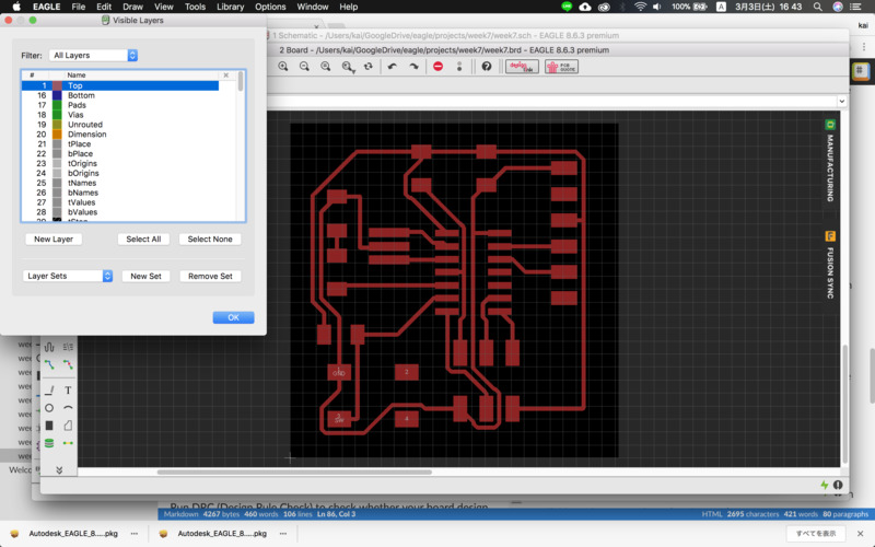
top layer (trace)
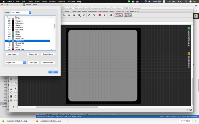
document layer (outline)
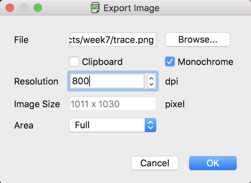
Export image
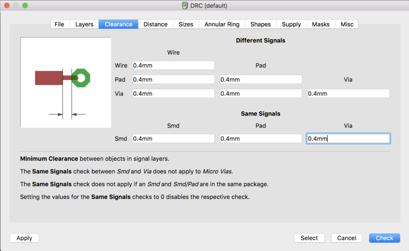
In the end, run DRC (Design Rule Check) to check whether your board design millable with your machine. (Tool > DRC)
As we use 1/64 inch bit, there should be more than 0.4mm clearance between each pattern. Change all clearance value in the dialog to 0.4mm and hit “check”.
Basic rules
- Place GND at the bottom, VCC above.
- Signal lines should flow from left to right.
- Connect wires directly as much as possible.
- No1 pin of chips indicated by round pin pattern or small dot.
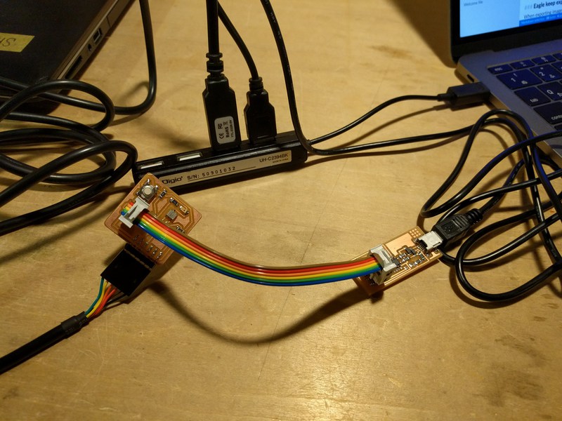
Mods, SRM, Soldering
I used SRM-20 for milling circuit, and made path data with Mods.
Refer to Week5 : Electronics production for detail how to’s.
Here is the results for milling,
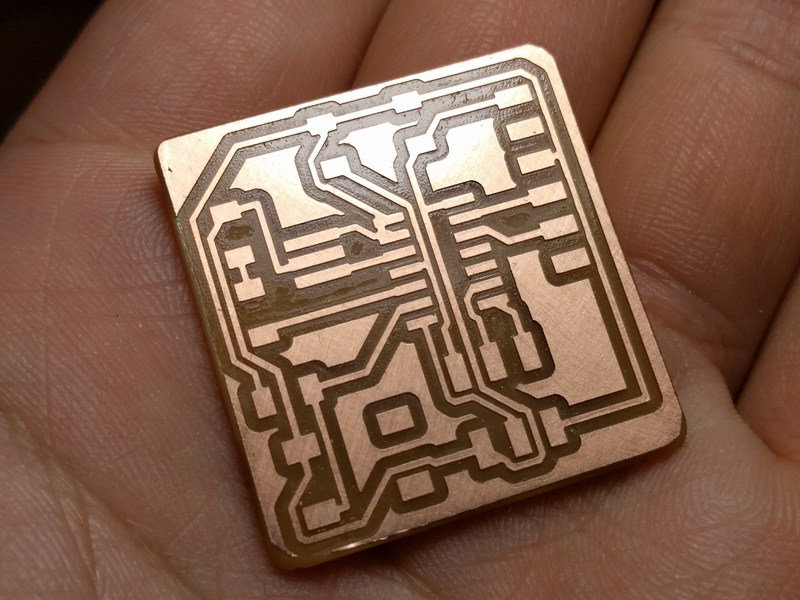
and after soldering.
Troubles
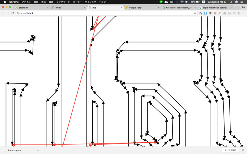
Eagle keep exporting wrong size
When exporting image from Eagle, despite of the the setting we had (Image size : 1011 x 1030), the exported png data had different image size (1028 x 1064).
We couldn’t figure out to fix this problem, so we changed the dpi after exporting data with preinstalled preview app in mac (enlarged 800 to 1600dpi).
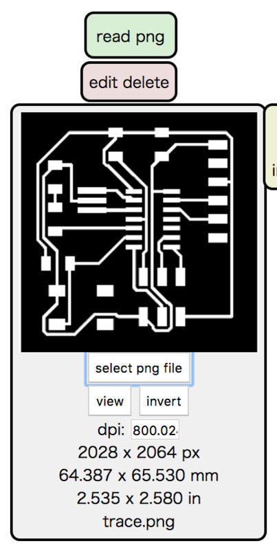
Mods doesn’t draw path between 0.4mm clearance
Although we checked the clearance with DRC, Mods couldn’t draw path between some gaps.
I solved this by setting milling bit diameter bit smaller then actual size.
Programming
Reference
Procedures
Preperations
-
Install ftdi chip driver
http://www.ftdichip.com/Drivers/VCP.htm
To get FTDI cable working, I had to install driver first. -
Download following files from class page, and put them in the same folder.
hello.ftdi.44.echo.c
hello.ftdi.44.echo.c.make -
Install pip
Download get-pip.py and move to the same folder as above.
Then run…$ sudo python get-pip.py
Now, you will be able to install pyserial by doing…
$ sudo pip install pyserial
Connecting boards
Program your board
Then follow the instruction in programming. You may find the link in week 8 class page too.
Go to directory you placed the files.
then run following command on terminal to compile program and write it to the board.
$ make -f hello.ftdi.44.echo.c.make
$ sudo make -f hello.ftdi.44.echo.c.make program-usbtiny-fuses
$ sudo make -f hello.ftdi.44.echo.c.make program-usbtiny
By doing this, you will get .hex and .out file in your folder.
If you want to progaram your board with other programmer such as AVRISP, replace usbtiny with avrisp2 like this…
$ make -f hello.ftdi.44.echo.c.make
$ sudo make -f hello.ftdi.44.echo.c.make program-avrisp2-fuses
$ sudo make -f hello.ftdi.44.echo.c.make program-avrisp2
You may find the term you need to replace, by checking hello.ftdi.44.echo.c.make file.
Communicate with your board
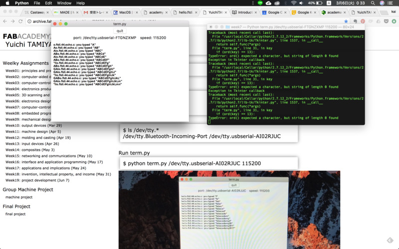
Now, try run term.py program to communicate your board.
First get serial port information
$ ls /dev | grep usb
or
$ ls /dev/tty.*
Run term.py
$ python term.py /dev/tty.usbserial-AI02RJUC 115200
cf) $ python [file name] [serial port][speed]
hello.ftdi.44.echo DEMO from kai naito on Vimeo.
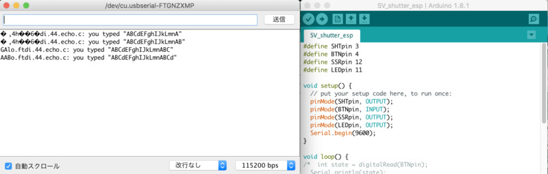
Serial communication via ArduinoIDE
You may also use ArduinoIDE Serial monitor to communicate with your board once your board is programmed.
- Open Arduino IDE
- Tool > Serial port
Select the port which the board is connected. - Open serial monitor by hitting button in the upper right corner.
- Type in some thing…