7. Electronics Design
I started this module by learning the basics of electronics online. We had covered some components in the Electronics Production module but it was good to expand on my knowledge. I read through several article's recommended by Emma including by Sparkfun and Make magazine.
Learning Eagle
The next day I moved on to learning Eagle. I worked through two of Jeremy Blum's tutorials (Tutorial 1 and Tutorial 2), which gave a detailed reference of how (and why) to use Eagle, both the schematic and board views. Understanding layers, component libraries and the making of routes was essential.
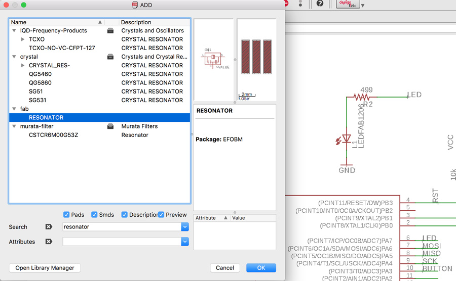
Eagle works has two views: schematic, where you search and attach components; and board, where you position the routing between components. The good news is Eagle is very user-friendly. To search for components, you use the 'Edit > Add' menu. Components can be searched alphabetically and are listed under specific libraries. Using the instructions from an Instructables tutorial I added two libraries for the FabAcademy and Adafruit were contained in these libraries. When you select a component, you initially place it roughly where you want it and continue to search for the next component. Pressing the Esc key you can cancel the search at any time. It is also necessary to place a component for VCC and GND.
When you have your components loosely assembled, there will be a lot of text labels. You can update these using the Name button, or delete them using a combination of Smash and Delete. It is useful to give resistors for example, a value (Value button) so that you can determine between them when working in board view and at the point of soldering. Names also play a role in linking components without visible nets (see below).
You can connect your components one of two ways: Nets, allow you to draw lines between each in a straight forward manner. Junctions can be applied when connecting multiple nets. Names, allow you to target a Net and virtually connect to another Net. To do this, you give the Net the same name (eg. MOSI) as the one you wish to connect to. Eagle gives you a warning and proceeds to virtually connect the two Nets.
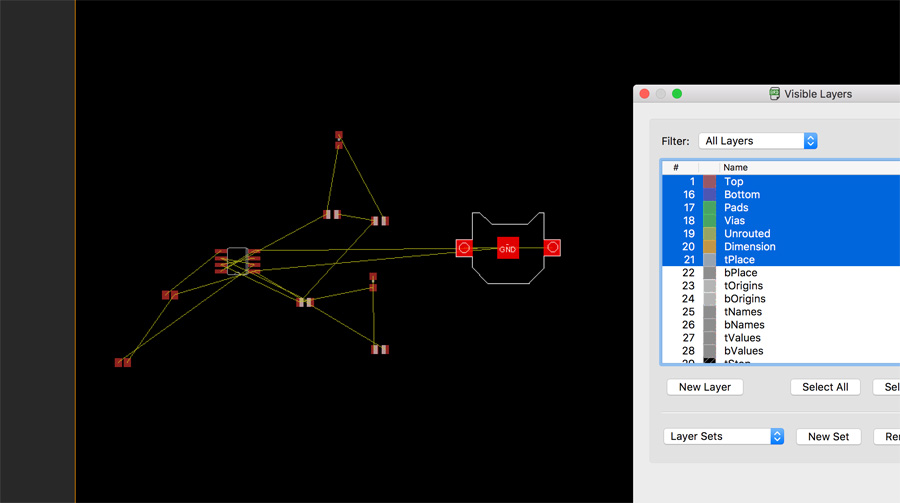
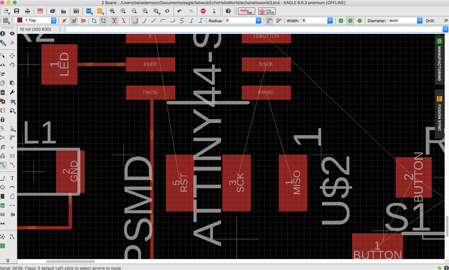
Both system create small yellow wire in Board view that help you route. In Board view (Available under 'File > Switch to Board View') you need two spread out your components, adjusting the board dimension using the Move tool. You then use the Route tool to create the position for copper routing between components, preferably with Wire Bend Style 1. Sometimes you need to rotate components in order to reduce routing. If you make a mistake, the Ripup tool can be used to remove the routing. Eagle is able to update the Board view when making changes to the Schematic, which is handy for troubleshooting.
Assignment
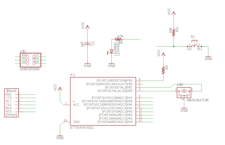
On the third day, I moved on to the assignment, matching components to create the appropriate schematic. I based my design on echo hello world from the Fabacademy lecture notes. I enhanced the board by adding a surface mounted (SMD) button and LED, to act as an inout and output. In total, the following components were added - made available at the Fab Lab Sorbonne,
- 2X03 Pin Header x1
- FTDI-SMD 6 Pin Header x1
- ATTINY44 x1
- 1uF Capacitor x1
- 10k Resistor x2
- 499Ohm Resistor x1
- Crystal Resonator x1
- 1206 SMD LED x1
- SMD Button x1
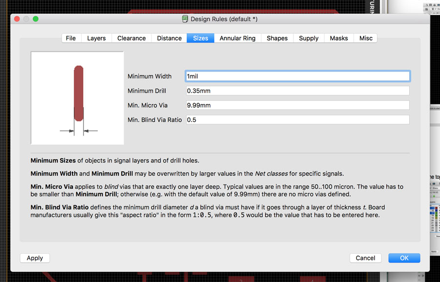
I experimented with the design rules and net classes to see how they would effect the board view. When I had to redo the board, I used the design rules to give a minimum width to the drill holes (0.35-1mm) but I later abandoned this idea because the smallest available cutting tool was 1.5mm.
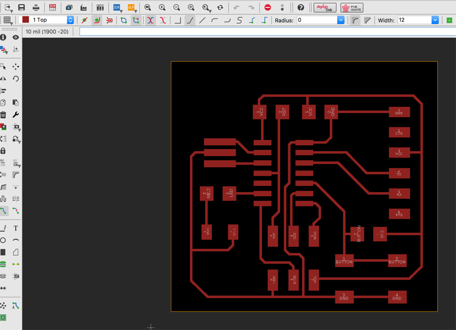
It took a good deal of time to lay out the schematic. By comparison, working with the board view was relatively straight forward. I manually routed the traces and used non-right angle corners, based on the recommendations. Routing at 45 degrees reduces the overall trace length and risk of acid trap (chemical etching). This is discussed in a datasheet from Texas Instruments.
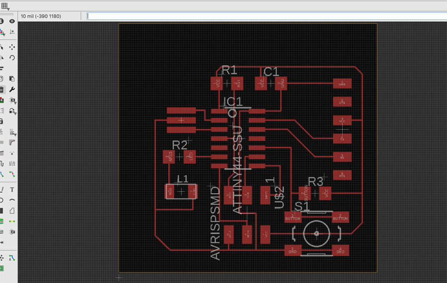
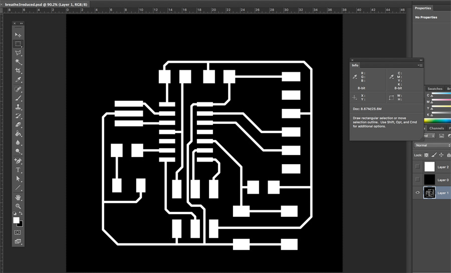
On a final step, it was necessary to add a rectangle on a blank layer (52 bDocu) to create an overall border – I made this quite large, approximately 10mm beyond the board dimensions. I exported my files as Image/PNG: The top (traces) file, selecting the top pad layers, and the cut (overall cut out) file, selecting the dimension and pad layer.
Photoshop
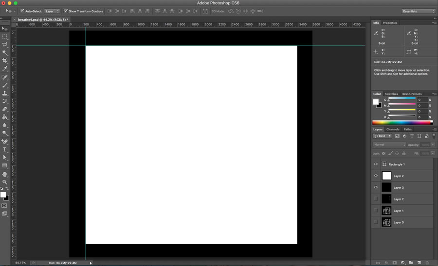
As with the ATTinyISP, it was necessary to invert the colour for the outline (cut) file. In Photoshop I used guides and the marquee tool to fill the cut file border with white. The file had been exported form Eagle at 1200, monochrome with a dimension of 3604x3364. I created a separate psd file and reduced the dimension by 50%, to 1802x1682. I exported the two files (trace and cut) as png files.
I would have to repeat this step several times due to errors with the dimension size and unknown borders in Fab Modules. Hidden guides in Photoshop potentially cause these borders - It was recommended deleting any guides (and any hidden layers) as a precaution.
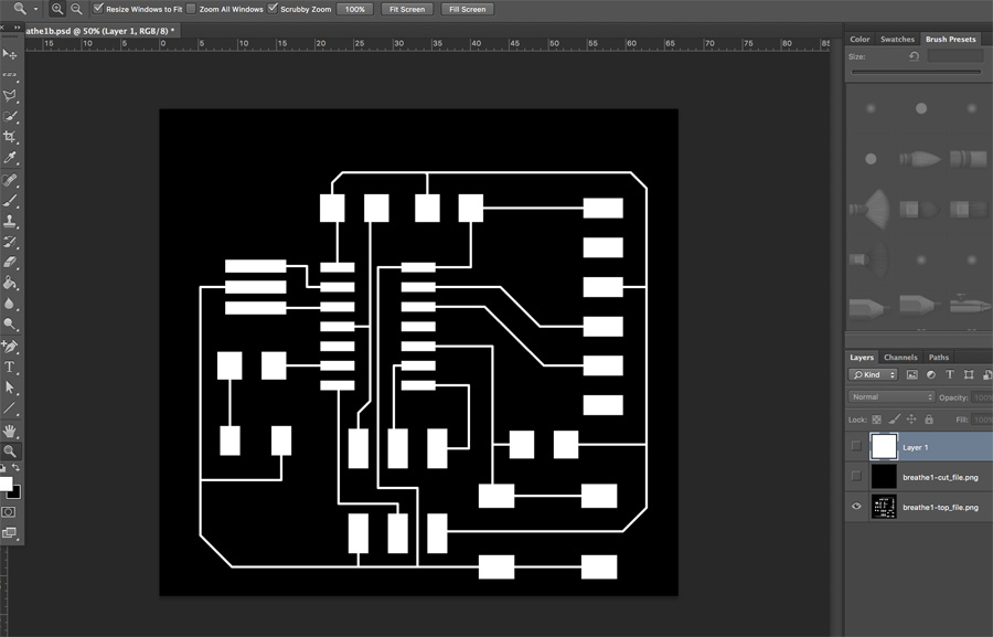
It was also recommended to redraw my traces under the ATTiny, where the traces run very close. By respacing and using more non-right angle bend (styles), I ran less risk of false connections.
In a final step, I double checked the distance between the mid-point of two pads twas in the region of 1.27mm.
Fab Modules
I imported the trace png into FabModules used the following settings for the top file:
- Machine SRM-20
- Speed 4
- X0/Y0/Z0
- Zjog 2
- Xhome/Yhome 0
- Zhome 20
- send command / server NO CHANGE
- tool cut depth 0.03
- tool diameter 0.4
- number of offsets 4
- offset overlap 50%
- path error 1.1
- image threshold 0.5
- sort merge diameter multiple 1.5
- sort order weight -1
- sort sequence weight -1
The tool diameter was later changed to 0.35 after issues with the routing on my second attempt. For the cut file I used the following settings:
- Machine SRM-20
- Speed 4
- X0/Y0/Z0
- Zjog 2
- Xhome/Yhome 0
- Zhome 20
- send command / server NO CHANGE
- tool cut depth 0.6
- stock thickness 1.7
- tool diameter 1.5
- number of offsets 1
- offset overlap 50%
- path error 1.1
- image threshold 0.5
- sort merge diameter multiple 1.5
- sort order weight -1
- sort sequence weight -1
I exported the two pngs as .rml files for the Roland SRM-20.
SRM-20
Much like with the ATTinyISP, I calibrated the X, Y and Z axis on the copper plate, making sure the plate was stuck firm and flat to the router floor. I used an average of the z depth between the approximate bottom-left, middle and top-left points. On cutting there was still some excess copper in places which I removed with a flat-edge scalpel. When I had to recut a new board for Embedded Programming, I had a lot more excess copper. I tried cutting with a new tool bit but it had slightly different dimensions and didn't cut well with my rml file.
I installed the previous tool bit and went went back to Fab Modules. I increased the number of offsets from 4 to 7. When I set the x-axis I made sure to pick the deepest value between bottom-left/ middle/top-left. There was still excess lines, particularly around the ATTiny pads.
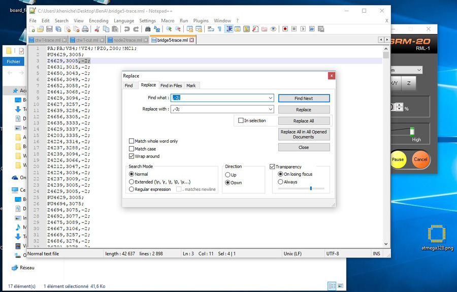
It's also necessary to check the g-code using Note++ on the PC (trace file only). This is because of a glitch in Fabmodules which outputs as '-2' instead of '-3'. If the glitch exists, you need to use Find & Replace tool across the whole file.
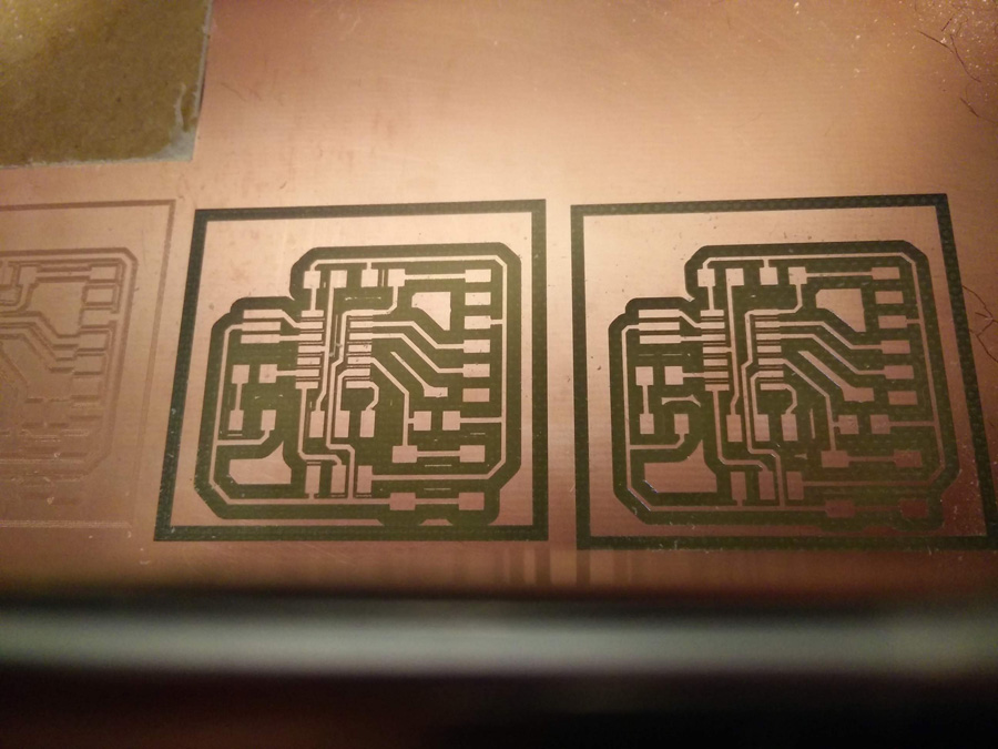
I tried decreasing the tool diameter to 0.35 and then 0.3 so there was no excess around the pads. This meant that the pads round the ATTiny would be hard to solder but at least there would be no false connection.
I swapped the tool bits, calibrating the Z-axis and ran the cut file in the same X/Y position.
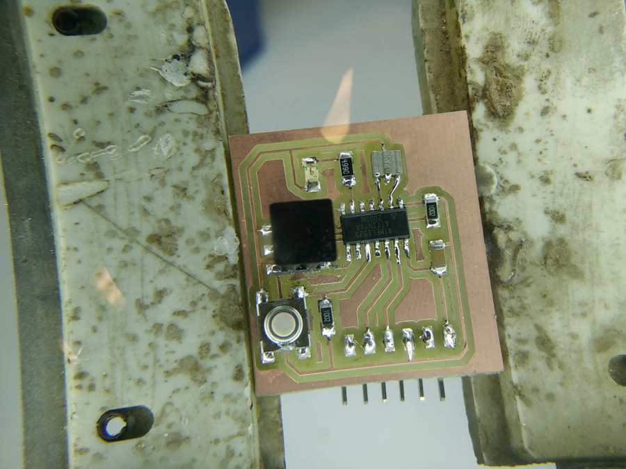
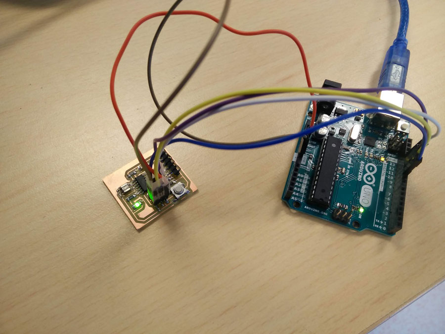
Soldering
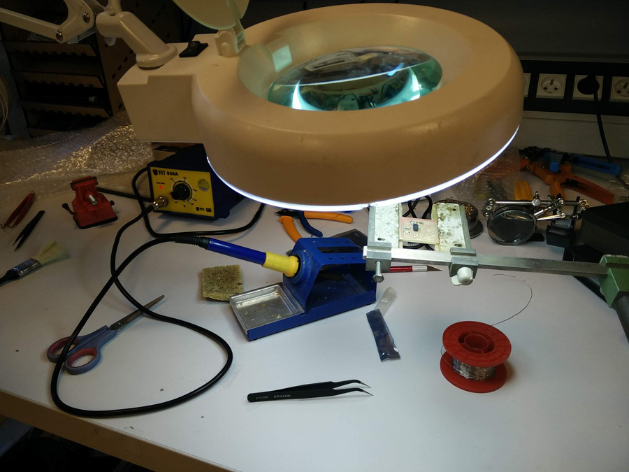
When soldering I used a slightly different setup, using the grips to hold the pcb in place as I soldered. A flat pair of good quality Weitus/WTS tweezers helped to position the components in place.
I gathered the following components
- LED 1206 (Red or Green) x1
- ATTiny44 x1
- 5k resistor (499 from drawer of 5K1 from folder) x1
- 10k resistor (from folder) x2
- 1.00uF Capacitor (1206 25V) x1
- XTAL Crystal Resonator x1
- straight vertical 4-pin
- right-angle horizontal 6-pin
- Press button
On the press button, there was an extra piece of metal running down the middle. There was some concerns that this would make contact with GND running under the button. I reviewed the data sheet and chose to cut the additional metal off with pliers.
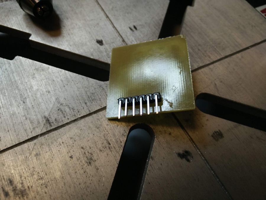
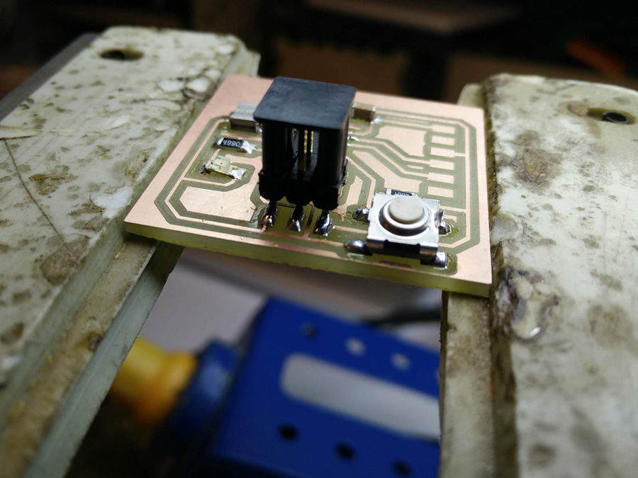
After soldering the various components to the board, it came to preparing the 6-pin. Knowing a 6-pin wire would be connected from the side, I chose to drill a small hole to fit the right angle through the board. After a few attempts on a test board, I drilled through the pads and soldered the pins from the top.
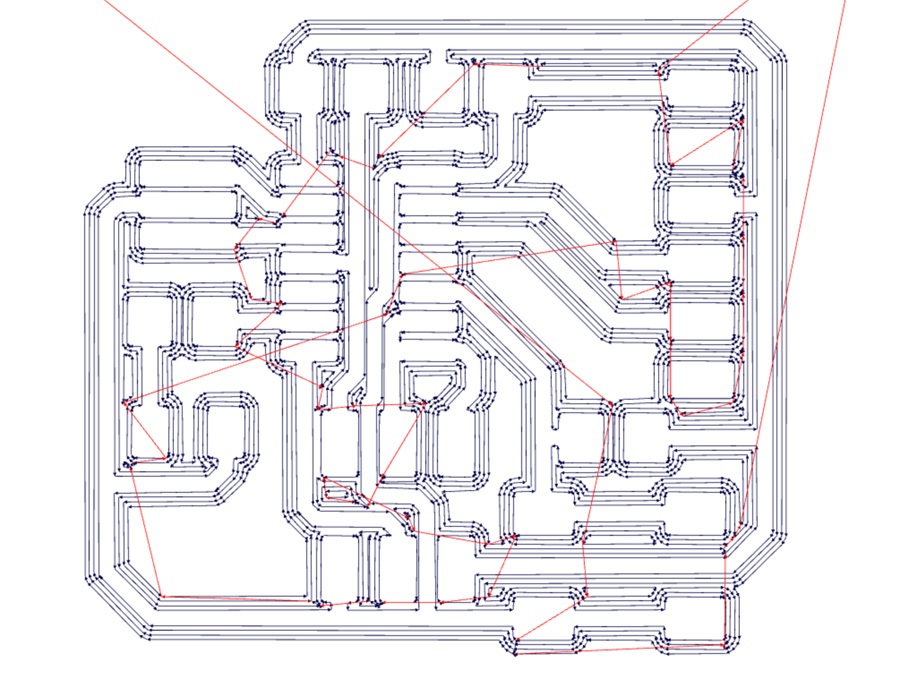
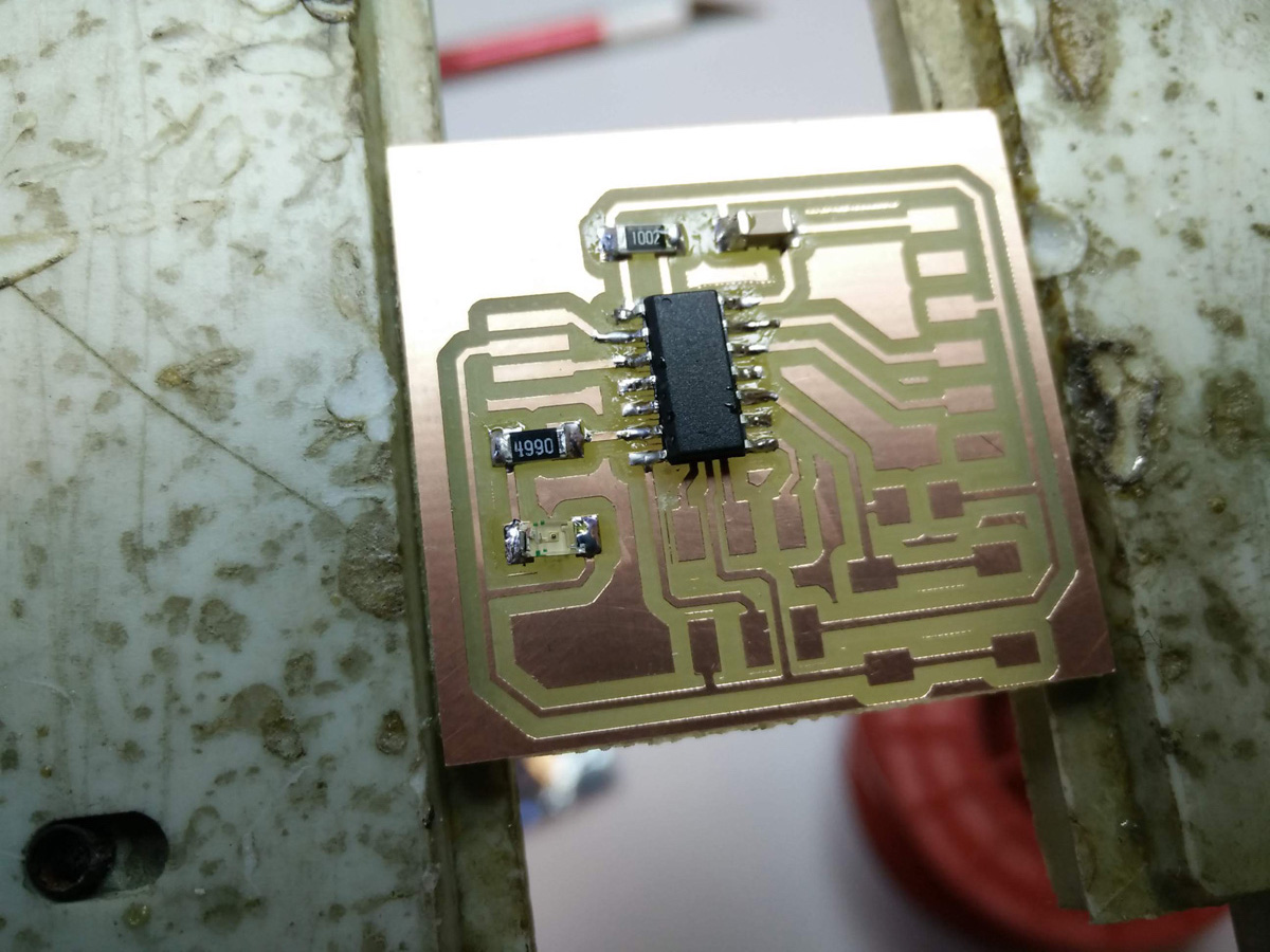
Routing Error
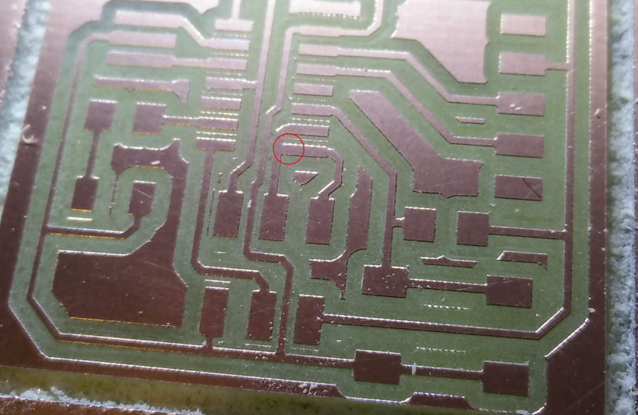
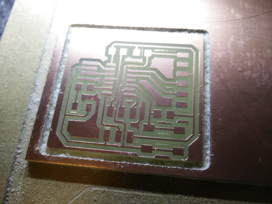
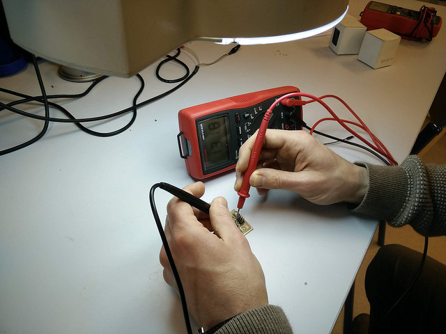
As described, the first attempt led to some clean soldering in comparison to the ATTinISP. I soldered the complete list of components but it was only when I tried to program my board that I realised there was an issue with my board. With my instructor Vincent, we used the multimetre to check connection on all components and the soldering was good. There was, however, a connection where there shouldn't have been – as shown in the image above – between two pads under the ATTiny.
There was no alternative but to redo the board in FabModules, reroute the board with SRM-20 and desolder as many components as possible. I found desoldering a particular challenge and managed to damage one ATTiny and crystal in the process.
Second Attempt
To separate the pads under the ATTiny, I had to return right back to the Eagle file and move the route lines further away. As outlined in the previous sections, hairlines of copper remained between the pads and I had to adjust the cutting depth several times.
With a fresh components, I soldered a little more 'smooth and shiny' than before. On my first attempt I was not well versed with how to use a multimeter. After a short introduction from Vincent, I took the time to check each connections after soldering. If the connection was weak, I adjusted the position of the component on the pad or added more solder to fully submerge the metal connection.
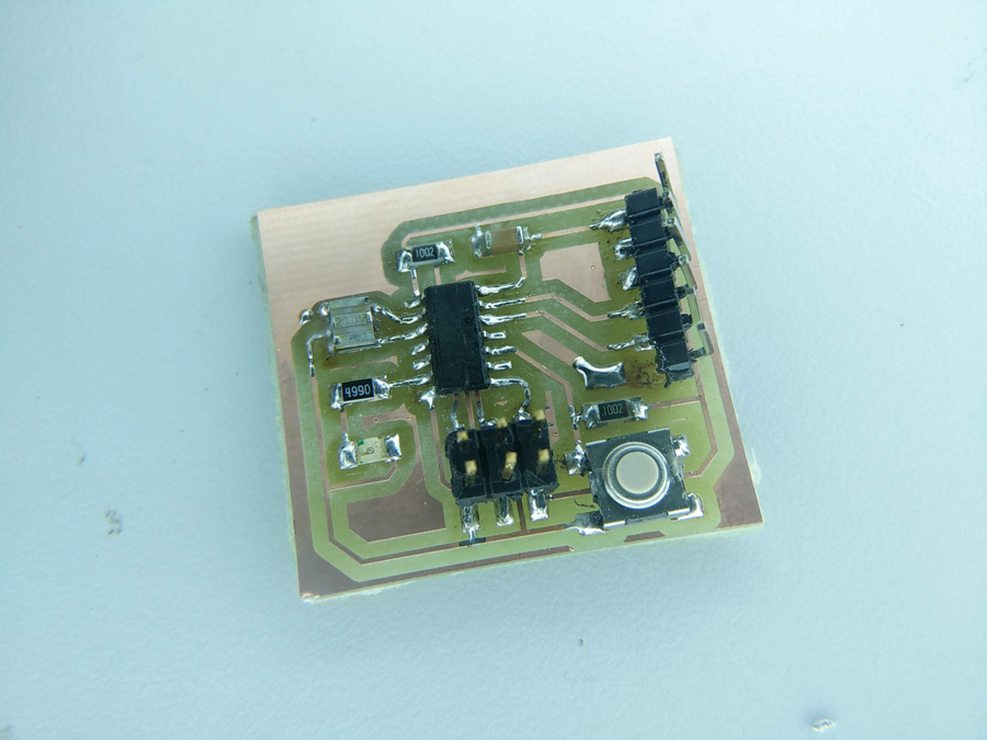
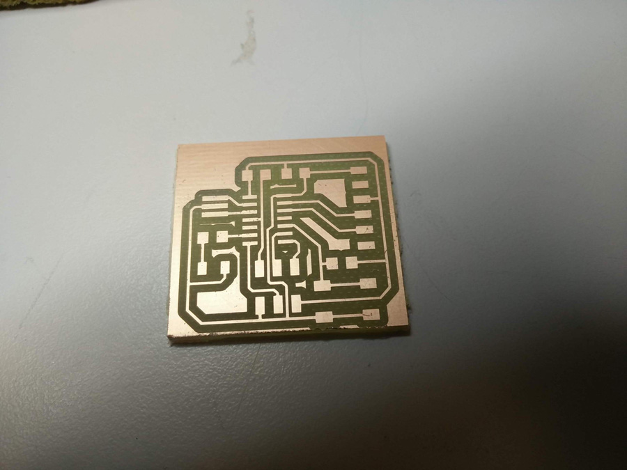
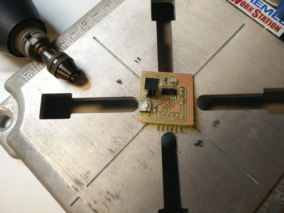
This time, I attached my six-pin connector by simply laying it on the board between routing. The overall board has less copper and thinner routing but all connections are sound. I uploaded a basic blinking program (File > Examples > 01 Basics > Blink) using the steps outlined on the week 11 page and it blinked! However, it blinked not as regularly as programmed. The feedback I received was that most likely there was a fault with the crystal.
I discuss using the oscilloscope on the Sorbonne group page.
Back to the top