This weeks assignment was to redraw and produce the hello echo board, while adding at least a LED with current limiting resistor and a button. We used an oscilloscope to measure digital signals for the group assignment.
What's on the board
As in the assignment two weeks ago, we need the following tools to make this board:
- A PCB mill
- A soldering iron
- Soldering tin or (preferably) soldering paste
- An ISP to program the microchip
Additionally, we need the following components:
- ATTiny 44
- 10kΩ resistor
- 1kΩ resistor
- 20MHz quartz
- 2x 33pF capacitor
- 100nF capacitor
- 3mm blue LED
- 4mm button
- 2x3 pin header
- 1x6 pin header
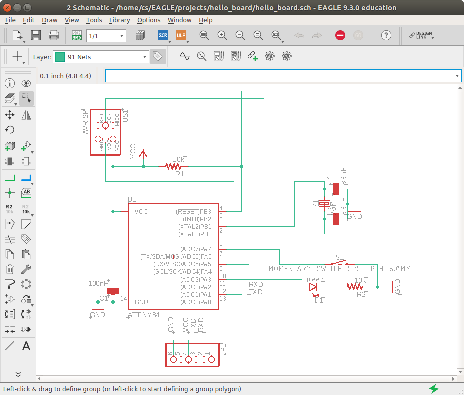
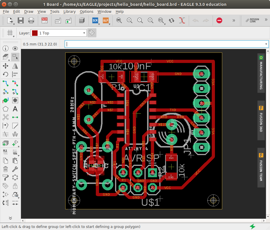
The board design is mostly taken I did not use SMD components exclusively, mainly because we did not have the quartz available as an SMD component, and I didn't want it to be the only thing on the back side of the board. Instead, I put the quartz and all parts that need to be interacted with on top of the board, and the SMD parts on the other side. The quartz, together with the two 33pF capacitors, constitute a resonator that the ATTiny may use as an external clock. The 1x6 pin header can be used to connect the board to other boards via serial connection.
I added a button and a LED (together with a current limiting resistor) to the board and connected each of them to one of the multi-purpose pins of the ATTiny.
Drawing the board
I used Eagle to draw the boards schematics and layout. Since I was already used to Eagles peculiar user interface, this part was pretty straightforward, except for the routing. This took me some time to get right, because in the original design, the ground line has to be routed through the pin header beside another route, and both the LED and the button I added have to be connected to ground as well. I added holes in the corner of the board because I wanted to print a case for it, but I noticed that they are probably too small to be used with 3D printed parts.
Making the board
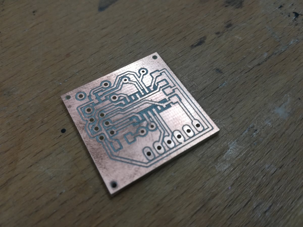
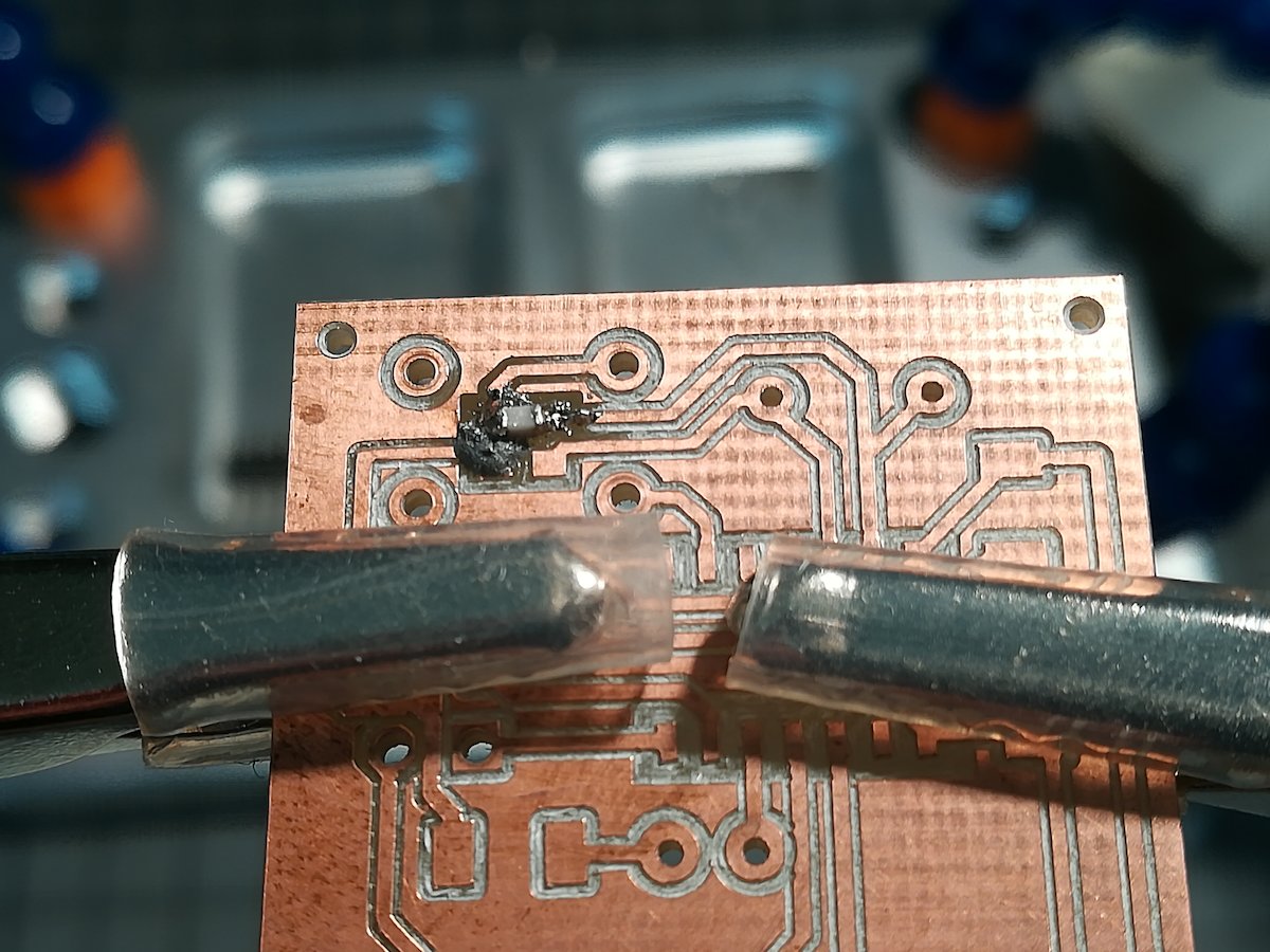
The milling process is analog to the milling process for the FabISP: loading the board in CircuitCam, adding outline and rubout, milling with Board Master. The soldering part was considerably easier than for the FabISP, because this time, I separated the small SMD components from each other, and, in my opinion, through-hole-components are generally easier to solder.

Addendum: Eagle Tips & Tricks
In the further course of the Fab Academy, you will have to make a lot of boards. At least I had to. And if you're using Eagle, like me, you might find yourself frustrated at the inconvenient interface (like me). That's why I've gathered a couple of things here that have helped me get more out of Eagle (or at least, reduce frustration).
The Basics: Using the Grid and Libraries
The design of a PCB starts with the schematic (in the schematic view), where you specify the components on the board and their connections to each other. Then, you have to create the physical layout of the board (this is called routing) in the board view. Eagle does not allow you to change the components or their connections in the board view, you have to use the schematic for that.
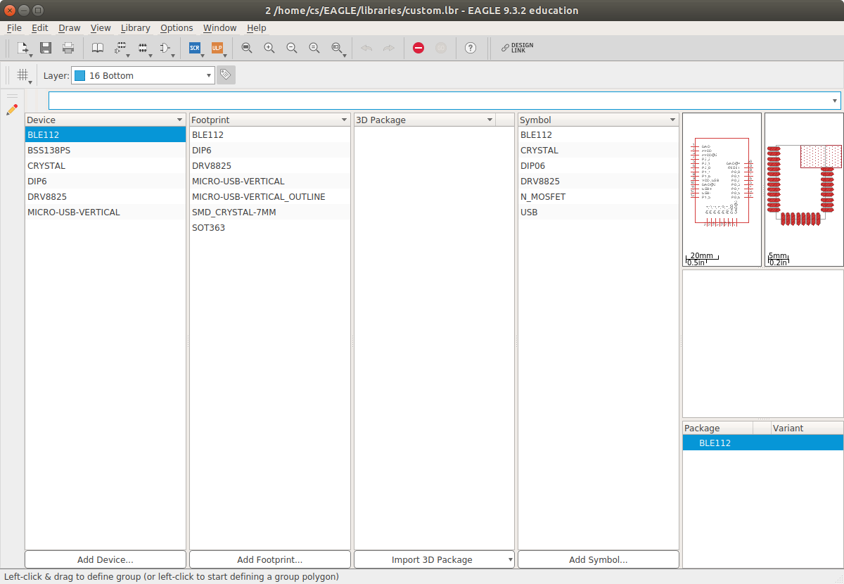
All available components are organised in libraries, which are shipped with Eagle, available online, or created by yourself. A device consists of a symbol and a footprint; the symbol represents the device in the schematics, and the footprint is placed on the board. There might be more than one combination of symbol + footprint for a single device. A device is added with the add part tool in the schematic. There is a search function in the dialog that opens with this tool, but I think it's not particularly helpful, since it pretty much only works well if you know the exact name of the device you're searching for. Nevertheless, it is worth a try if you don't know what to look for.
With the help of the library manager (accessible for example from the add part dialog, for example), you can install additional managed libraries; these get updated automatically, so they are preferable over similar ones downloaded from the internet (All of the Sparkfun libraries are there, for example; no need to download them oneself).
The absolutely most helpful tool for designing board layouts in Eagle is the grid tool, in the upper left corner. Don't be afraid to use it frequently when placing components on a board. I set it to 0.5mm/0.1mm, line style display, always on. Pressing Ctrl when selecting an object with the move tool will align the object with the grid, and holding the Alt key while moving will use the alternative grid to allow more fine grained control over positioning.
You can save a grid alias for easy access to often used grid settings.
Either right click on the grid button and choose "New..." to create an alias with the current settings, or use the command line and type in grid = name @, which will create and alias named name.
The alias can be set with the command grid name.
To change the default grid that Eagle starts with, you can change your eagle.scr script in your scripts folder (In linux, this can be found at ~/EAGLE/scripts/eagle.scr).
For example, add the following under BRD: (which are settings for the board editor):
Grid mm 0.5 lines on alt mm 0.1;
This will set the default grid to 0.5mm, lines on, with an alternative grid of 0.1mm.
Use the command line
One observation I've made is that sometimes, the command line is the only way to get things done, or it's at least a lot easier this way.
For example, imagine you just have made a design with 8mil traces.
You notice you have enough room to have 12mil traces, and that would make the board more reliable.
Now, how to change the width of all the traces?
You could rightclick every signal line and change the width property, but that would take forever.
Instead, use the group tool (the default tool) to select all traces, enter change width 12mil, hold down the control key and rightclick.
Tada!
Generally, entering a command is like selecting a tool: clicking on a thing applies the tool/the command to that thing. If you have selected a group of things, holding ctrl and right clicking will apply the tool/command to all elements of the group.
Usually you don't have to select the command line to type in commands; if it is greyed out (i.e. inactive), press Ctrl+L to select it.
Which commands to use for certain actions can be figured out by trial and error.
Generally, tools have a corresponding command, e.g. move to select the move tool, route for the route tool, net for the net tool, etc.
Properties can be set and changed with set p and change p respectively, where p is the name of the property.
Dimensions specified without units are assumed to be given in whatever you set your grid to (for example, if your grid is set to mm, set width 0.4 will set the width to 0.4mm).
Particularly useful commands are, in my opinion:
help cmddisplays help on the command cmd.set width xandchange width x, where x is a number with optional unit, e.g. 8mil or 0.2mm (no spaces). This sets/changes the width of traces in the board design view.hole xwhere x specifies the drill diameter creates a hole to place on the board.smd XxYcreates an SMD pad in the footprint design view of size X times Y. To change the size afterwards, usechange smd XxY.name Xwill give the next thing you click on the name X. Since names have to be unique, I often use justname, which will display a field to input a name.grid xandgrid alt xwill set the grid distance and the alternate grid distance to x, respectively.grid Lasttoggles between the current grid setting and the previous grid settings.grid = alias @saves the current grid settings as alias.grid = aliasdeletes this alias.grid aliasuses the grid settings saved as alias.polygon siglets you create a polygon in the current layer, which is attached to signal sig. This is particularly useful to create ground & power planes. I recommend to set the isolate parameter of your ground planes to at least the diameter of your milling bit, to ensure your traces get milled with the correct width. You can do that by usingset isolate x; polygon sig, where x is the diameter of your drill bit.
Make your own Devices, Symbols, and Footprints
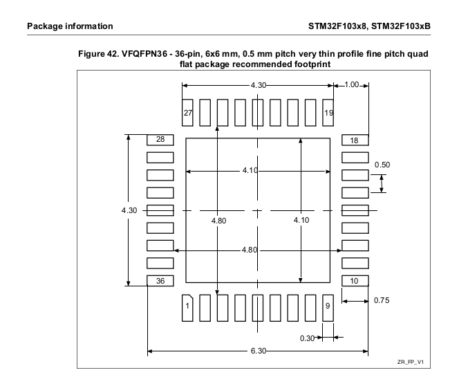
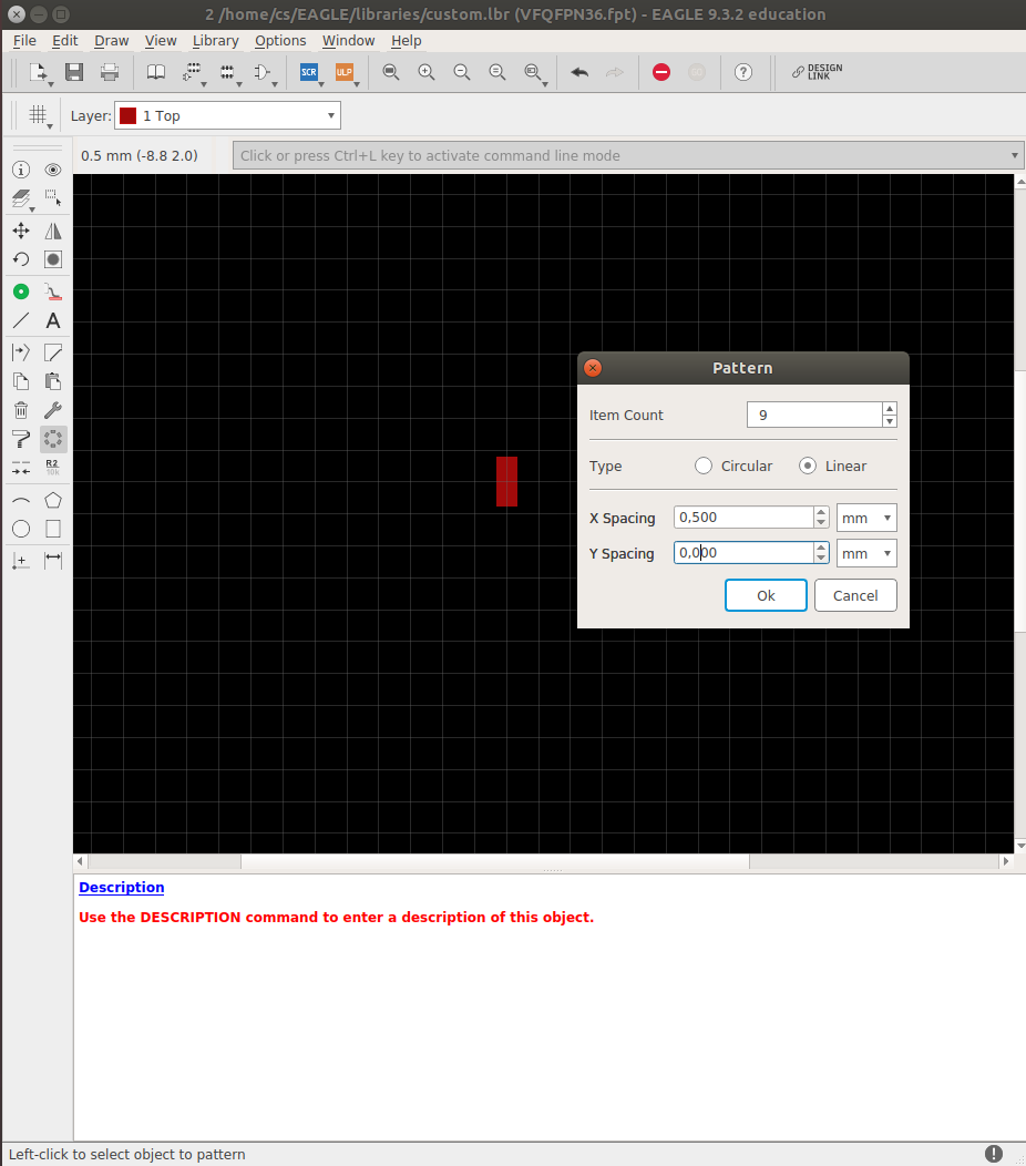
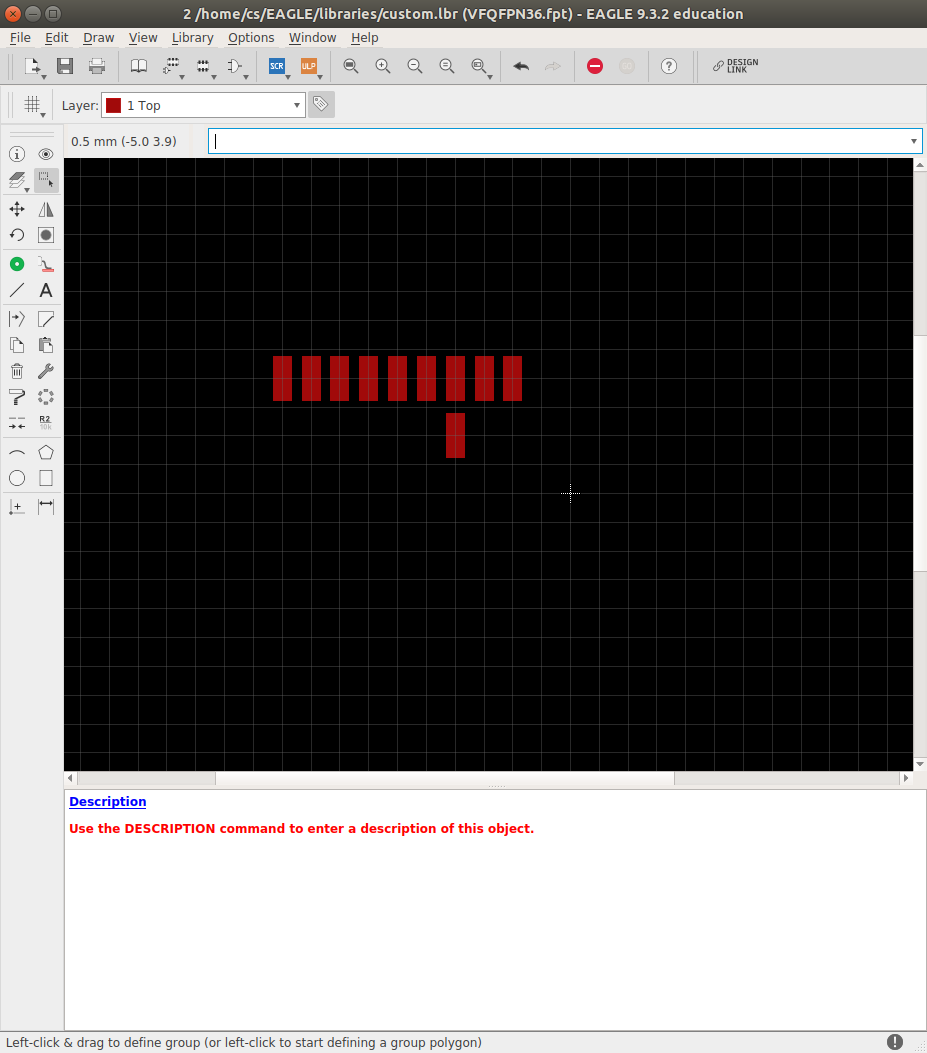
If you can't find the device you want to use in neither the standard libraries nor online, or you want/have to make changes to a device, you can roll your own. It's not difficult. First, add a new library in the control panel. To create a new device, we need to add a symbol and a footprint, which are then connected to each other to form a device. In the gallery at the end of this section, I've detailed the steps of creating a footprint for an STM32F103 which I need for my final project.
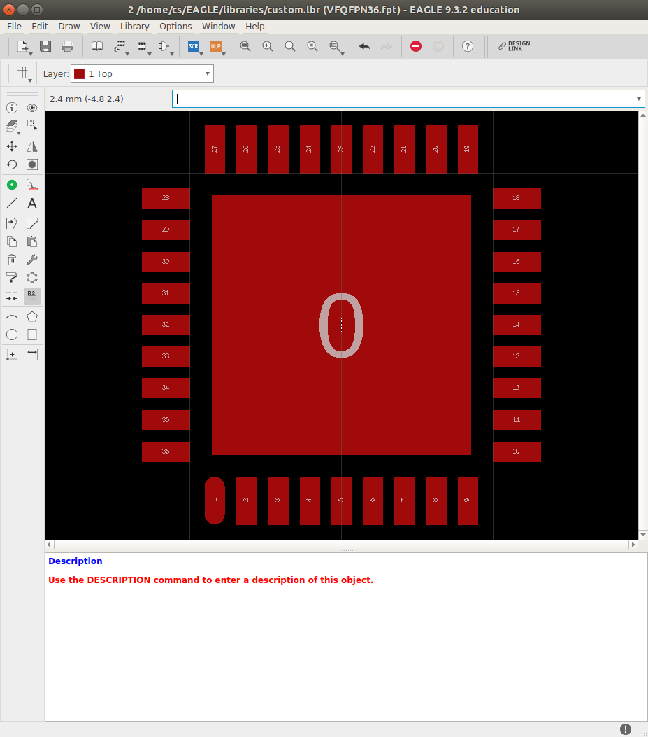
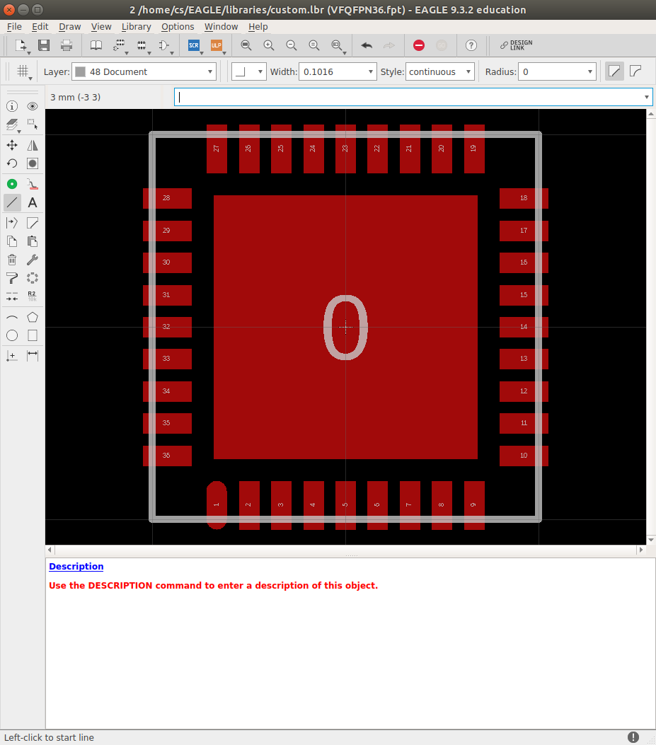
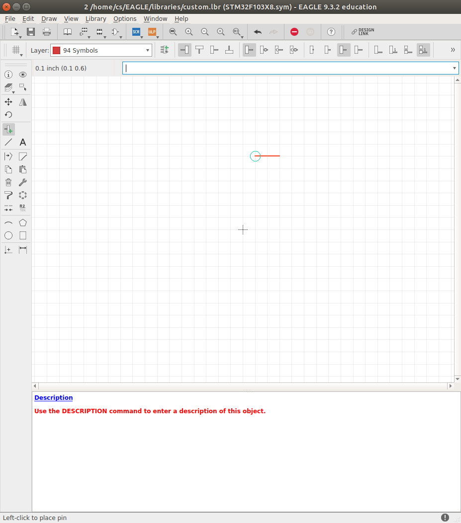
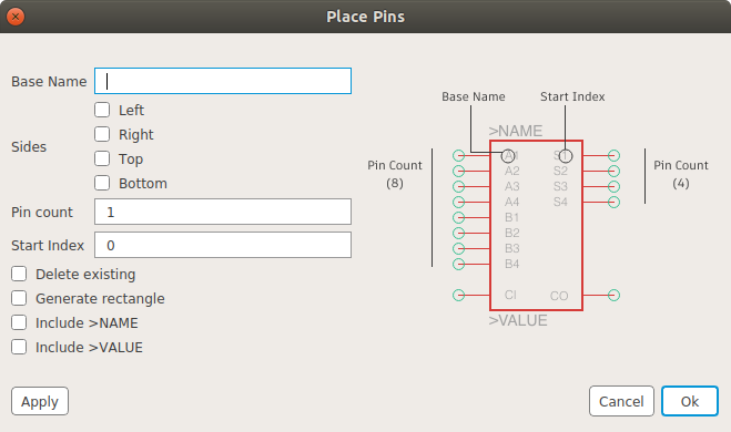
So, find the recommended footprint in your devices' datasheet, and click on "New Footprint" in the library editor. A particularly useful tool when making footprints for devices with lots of pads is the "smd array" tool (or "pad array", for through hole components), which can be accessed after clicking on the smd tool (or pad tool, respectively). Make sure to give the pads names that are in accordance to the devices datasheet. It is often helpful to mark the position of a device in the "tPlace" layer. To create a symbol, click on "New Symbol". For each pad/connection to your device, create a port, and give it an appropriate name.
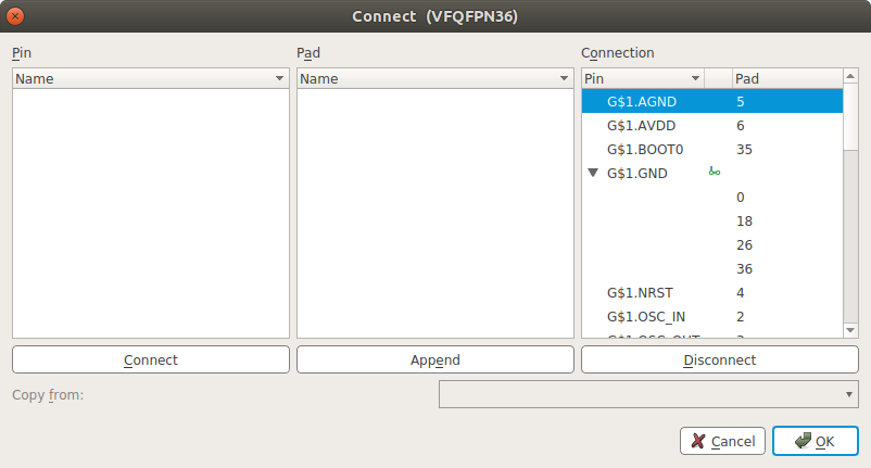
After creating a symbol and a footprint, you can create a device by clicking on "New Device". Then, add a symbol (or more than one), and a footprint (or more than one). The symbols together constitute the device, while each of the footprints represents a different package for the device. Thus, the footprint must have at least as many pads as there are pins on the symbols you added. Then, click on "Connect" to assign symbol pins to the corresponding footprint pads. You can assign multiple pads to a single pin by clicking "Append".


Design Rules
You can specify certain rules like minimum distance to board outline, minimum and maximum diameter of vias and pads, or minimum distance between signal lines as design rules. Eagle is checking these rules automatically; you can check for violations by clicking the yellow triangle in the lower left corner. Setting these rules in accordance to the machinery in your lab is an easy way to make sure that your designs will come out the way you designed it, even when creating very small, densely populated boards. I recommend setting at least the minimum distance between signals (under the "Clearance" tab) and the minimum drill size (under "Sizes") to the size of the smallest end mill and drill bit of your machine, respectively. Also, every time you add a polygon, set the "isolation" property at least to the value you chose for clearance.
Design rules can be saved in a design rule file (*.dru). Most fab houses/PCB makers will provide you with a design rule file for their production process. I've created a design rule file for the LPKF mill in our lab; for example, I've set the minimum distance to 8mil (instead of the standard 6mil), because the smallest milling bit that we use is 0.2mm (equals roughly 8mil) in diameter.