Overview
I had no experience with this before, so I started from scratch. I decided to use Eagle because it was recommended by the other students and instructors. I am able to work with it now, but halfway through I got the tip to use KiCad the next time, as it is easier for beginners, open-source and also powerful. Especially the standard library of parts is much easier to find what you need.
I decided to change to already existing echo hello world PCB from the FabAcademy. Sparkfun has really good tutorials for eagle to get to know what you need to do. The basic workflow of Eagle is: First you create a schematic (circuit diagram), which is just the description of all the electronic components you want to use and how they are connected. Afterwards, in a second step, you create a board layout from these parts. But now you already have all the parts available from the schematic do and "only" need to arrange them on the PCB.
But before I went into the creation I went into some research on how to add a button and LED to extend the existing design. A LED will get too hot if you don't limit the current that is flowing through it. A very extensive tutorial to LED's can be found on sparkfun, then you will know everything you want. When using a button connected to a microcontroller you want to use a pull-up resistor because with this you void a short circuit and have well-defined inputs when the button is closed and when it's open. I also decided to remove the quartz, as just the LED and button would not require a clock this accurate.
Designing the schematic
I started with opening the image of the echo hello world board as a reference to work along. After opening eagle, you need to create a new project and then add a schematic to this new project. Before you start you should download the eagle libraries for usb and fabacademy and put them into your eagle library folder (This can be found in Options->Directories in the main eagle windows). I followed this tutorial to create the schematics and will explain the most important parts, changed things and show some new screenshots in this chapter.
The first part of designing the schematic was for me adding all the parts to the board and afterward wiring all them together. Of course, you can mix them as you like.
Adding parts
When you clock on the add part button you can add parts from a huge list. Also, you can click on Open Library Manager in this window to see all available libraries and load more (like the fabacademy library for example). For every part, you get the schematic and board symbol shown to decide which of the versions of the part you want.
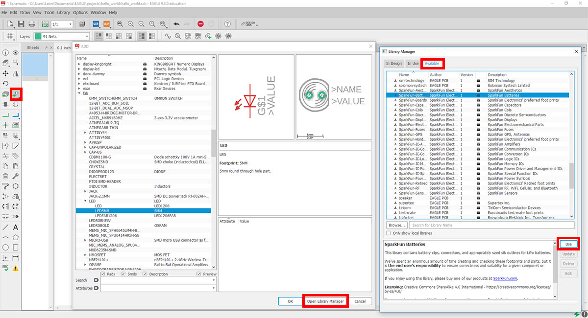
Adding parts and library manager
After Clicking on Ok you can click anywhere to place the part there. Or repeat the process to add other parts. One big drawback of eagle is the huge library of parts, which have cryptic names and you never know which to use. My tip: The fabacademy library already has the most needed parts predefined and the rest can be found by searching for it - the search field uses regular expressions, so make sure to search for *led* if you want to find all led's. Regular expressions (regex) are a way to match strings and be very precise for what you search for. An example for the use in eagle is that if you search for led, you will find all parts that have the word led in it somewhere, separated from other words by spaces. If the part would be named led2, it wouldn't find it. So the asterisk * is a symbol to match any letter. So by searching for *led*, you will also find led2. Another hint is the Sparkfun library, which is clear categorized and has a lot of parts.
To move parts around the workspace you need to select the move tool on the left side, left click on the cross of the object you want to move and then click to the position you want to move it. Rotating, mirroring and deleting are working the same.
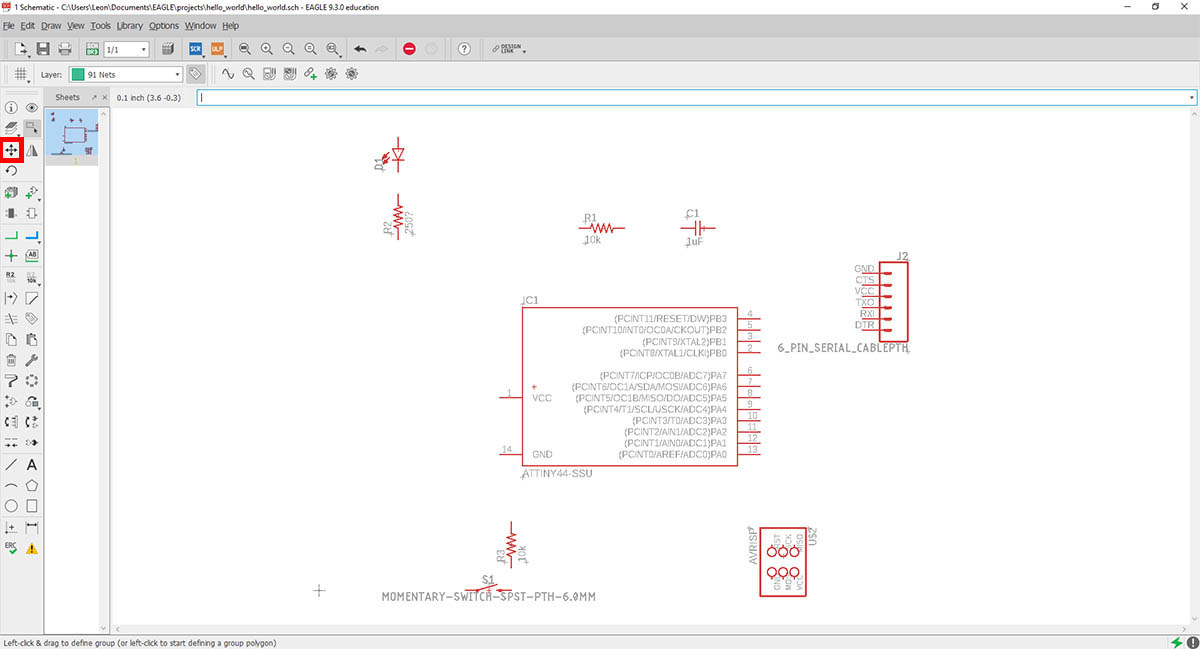
Eagle after adding all the parts
Connecting the parts
To connect parts together you can click on the Net tool. Then you click on the connector of a part, and then onto another. They get connected by a wire. You can also click on a wire, so the connector gets connected to this wire. This is indicated by a green dot on the wire.
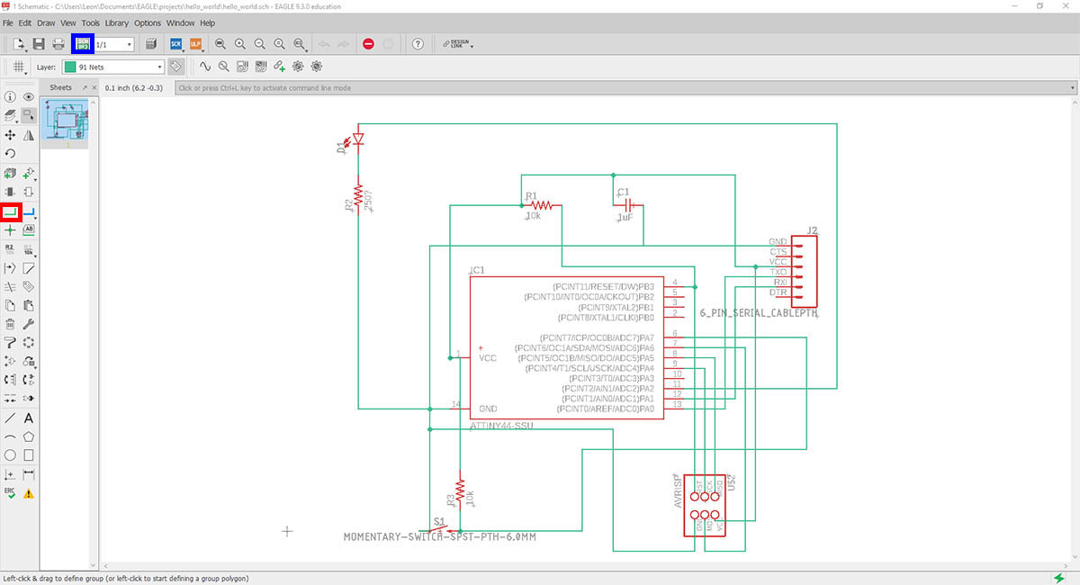
The finished schematic in eagle
Designing the board
After the schematic is finished the next step is to arrange all parts on the board. Here I mainly followed this tutorial. First, in the open schematics, you need to click on the button Generate/Switch to board, which is shown in blue in the last picture. Then you just get all your parts put into the board design tool:
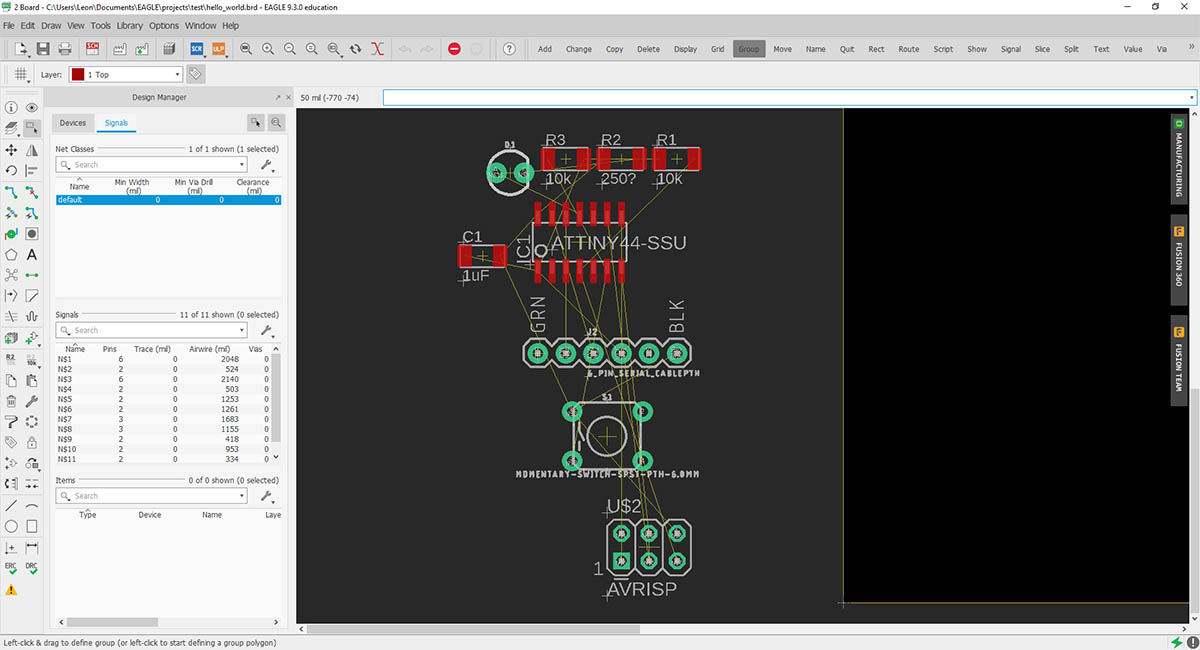
After switching to the board view
Moving the parts
First, the parts need to be moved and rotated to the positions they should be at, this is done in the same way as in the schematics view. Here the template is very helpful.
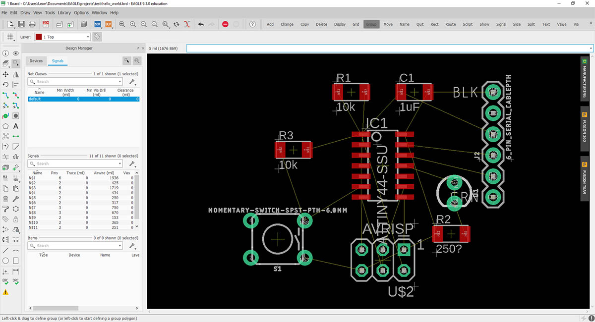
The arranged components
Routing the connections
Now the connections need to be routed. Therefore you can also mostly do the same as in the template, otherwise this step requires a lot of moving parts around. Similar to the connection in the schematics view, now you select the Route tool and click on one connector for one component. Now all the pads you need to connect this pad to get highlighted, so you easily see where you need to connect it. One thing that is useful here is when you click on empty area while routing, then the route up to this point will be fixed. That is helpful especially when adding complex lines.
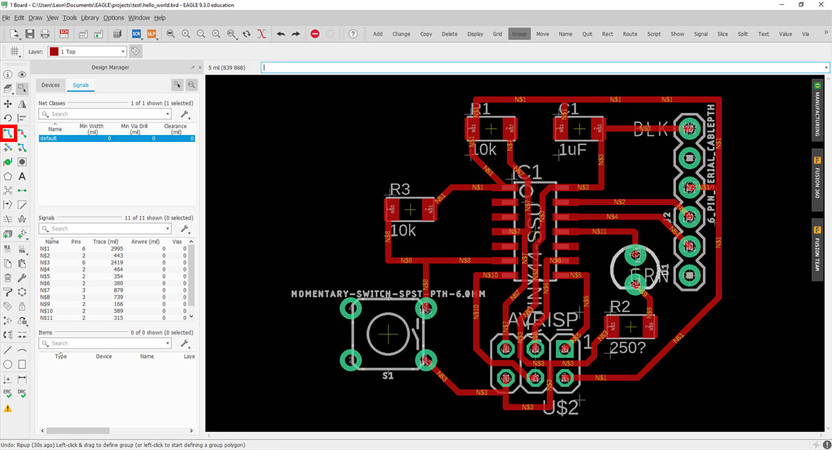
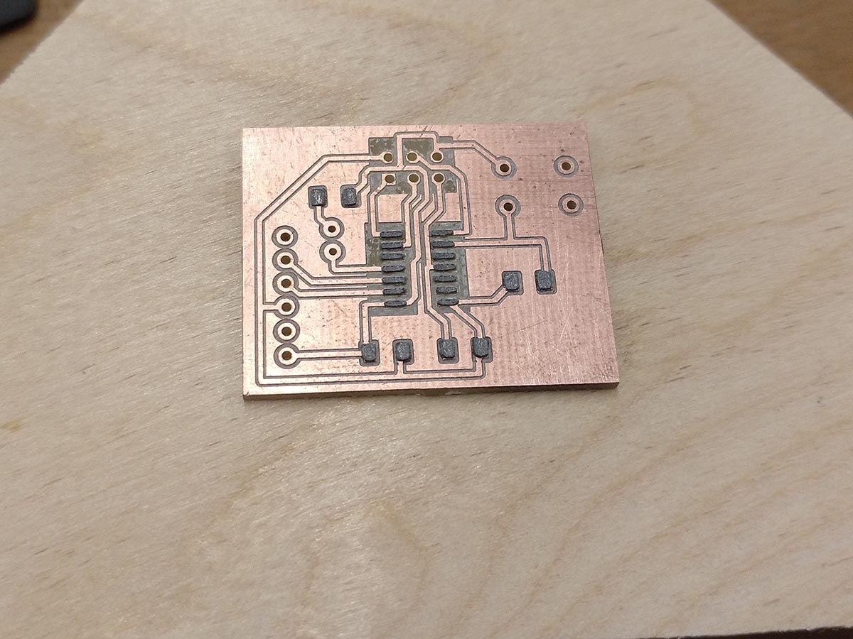
The routed PCB lines
Creating the outline
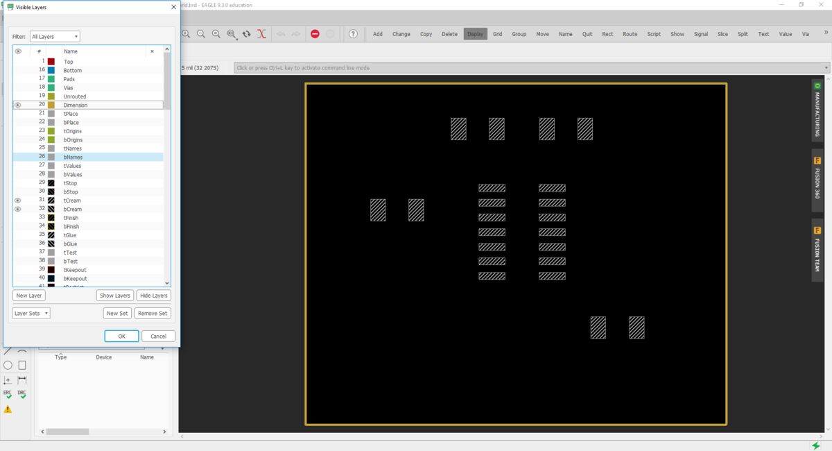
To create an outline where the board will be cut off you can use the line tool. But before drawing you need to change the layer to the Dimension layer.
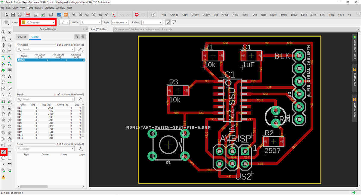
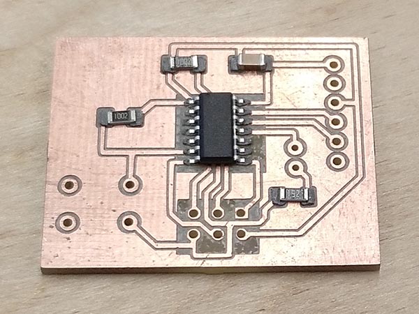
The finished eagle board
Checking design rules
Design rules are rules that an check if your board can be manufactured. After clicking on the design rules button you get a window where the design rules are specified. If you already know which i.e. clearance you need for your machine and soldering skills you can change the value there, otherwise you can just leave it on default and it will tell you if you did some mistakes.
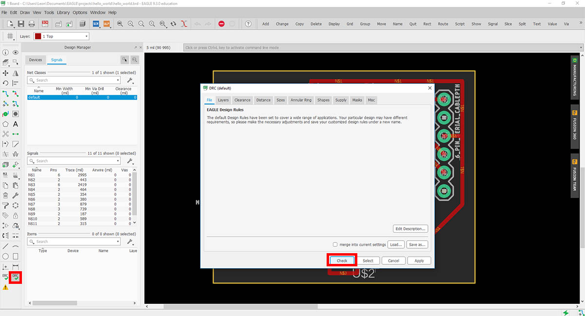
The design rule check window
For me, the program told me that there is a warning about a wire stub and it also showed me where. So I easily could remove this stub. In this case, it was not so important, because the stub was under the pad of a resistor anyway. But it is helpful to have an easy check if you did something wrong.
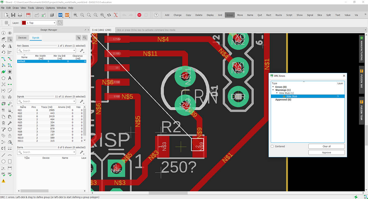
The design rule check results
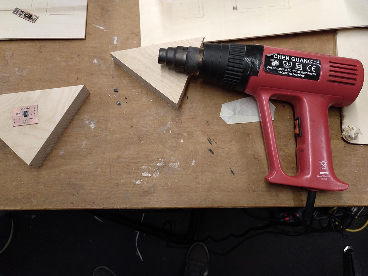
Milling
Our fablab has an excellent tutorial on how to use our PCB mill (LPKF S62). As there are several steps you need to take the tutorial is comprehensive, but it is best to work through it step by step when you want to mill a PCB. With this tutorial, my prepared eagle files and somebody watching me I was able to use the mill without any problems on the first try. I will outline the important steps, details can be found in the tutorial.
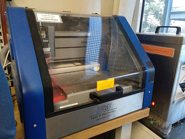
The PCB mill
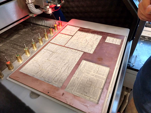
Putting a board in the mill
The first step is to copy the prepared eagle files to the pc next to the PCB mill. Then you start BoardMaster on the PC. Then you start eagle, export the created files using the CAM processor. These files you can open in CircuitCam for further editing. There you generate the outline, mark places where the copper is to be removed completely and export it to the BoardMaster milling software.
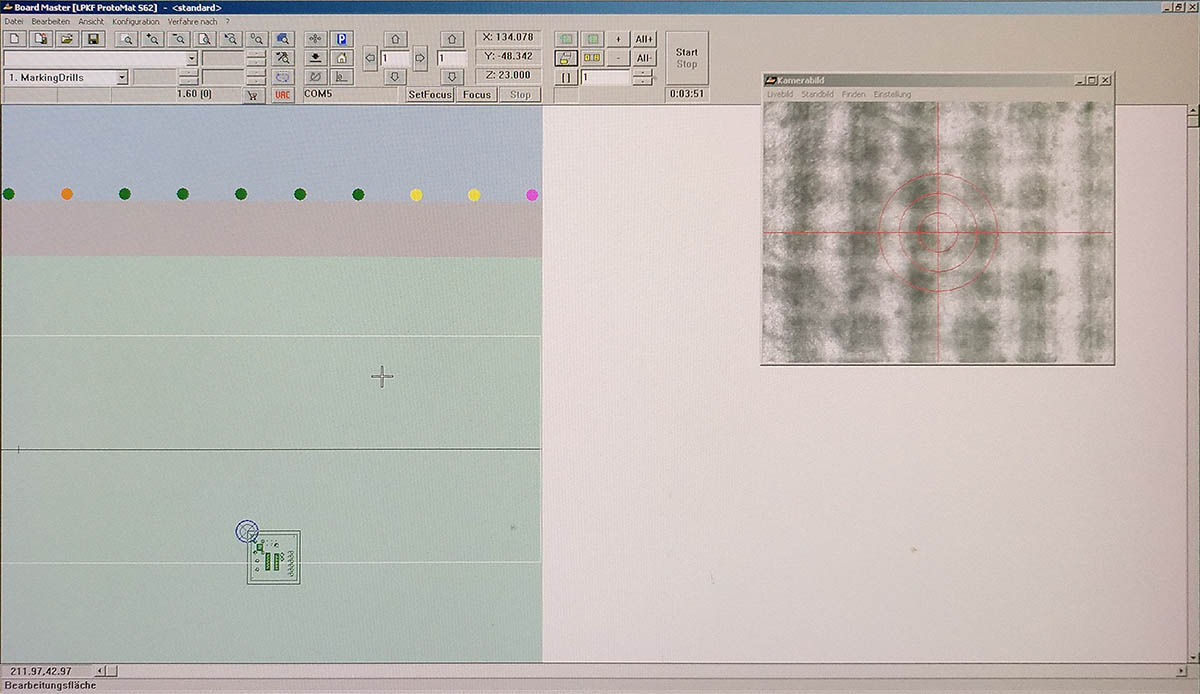
The BoardMaster software
In the program, you can see a camera image to place the milling head precisely. On the left, you can see the head position, working area and the PCB.
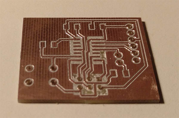
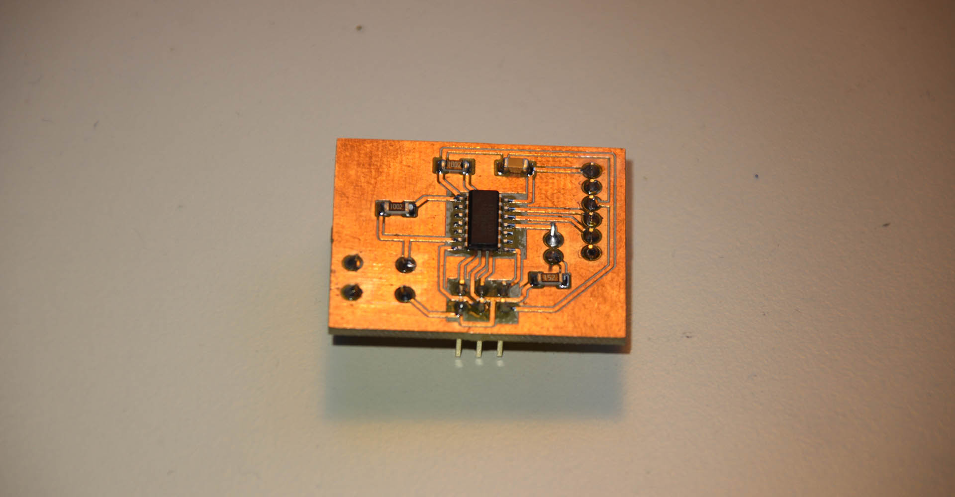
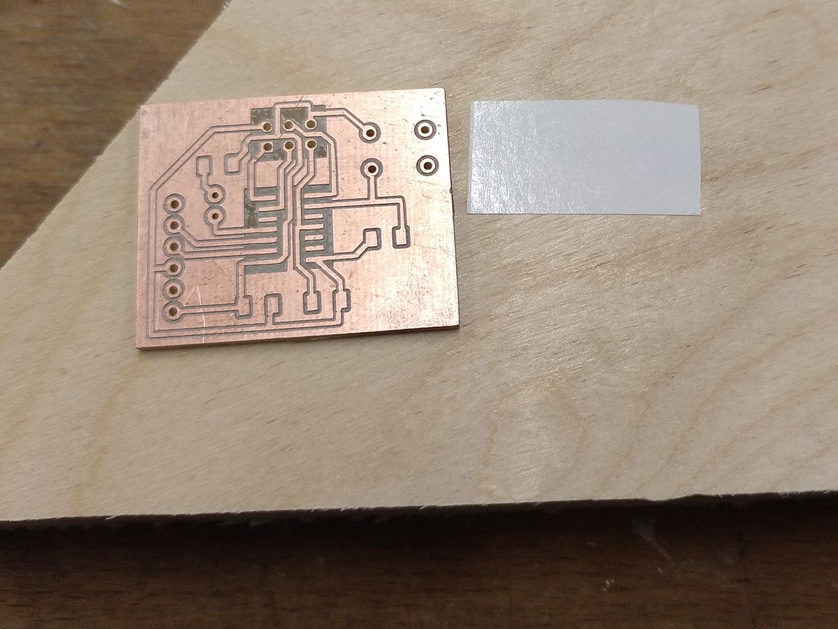
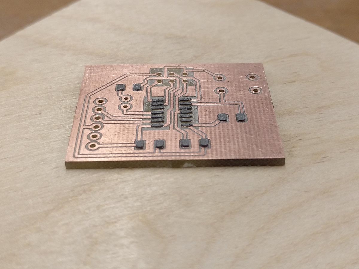
The finished board after milling
Soldering with a stencil
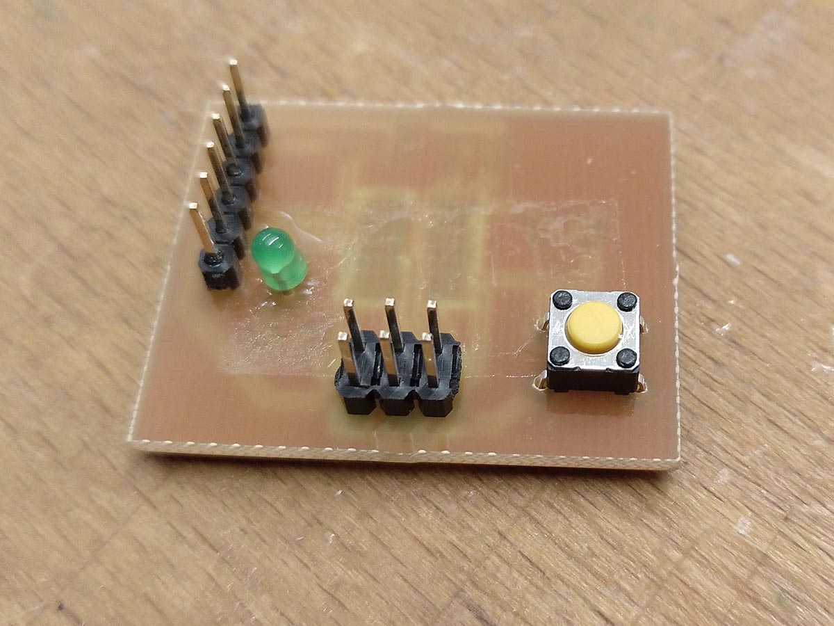
Bill of material:
-ATtiny44 (SMD)
-6x1 pin header
-2x3 pin header
-1uF Capacitor (SMD)
-2x 10kΩ resistor (SMD)
-250Ω resistor (SMD)
-LED (5mm, green)
-Switch (6mm)
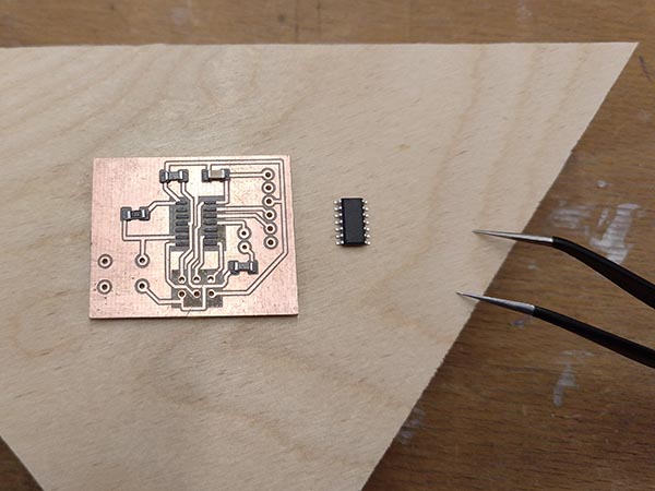
The parts for soldering
The last time I soldered the SMD components with a soldering iron and it worked but I was not too happy with my work. This time I wanted to solder using solder paste, a stencil and a hot air gun.
Creating the stencil
The basic steps to export the stencil from eagle are based on this article on the autodesk website. There is also a bit of information on stencils in general.
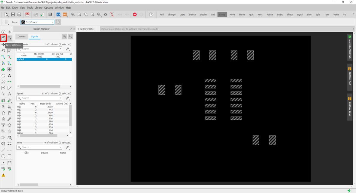
Click on the layer settings button to select the layers you need
Click on Hide Layers to hide all layers and select the three layers Dimension, tCream and bCream.
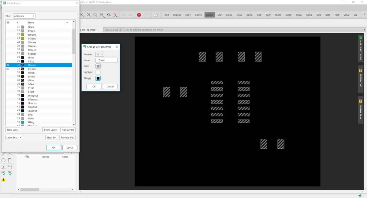
Double click on the tCream layer to change the fillstyle to something solid, otherwise the lasercutter will cut more than needed.
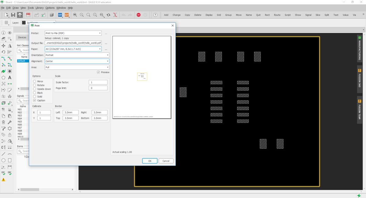
Print the board to file (PDF)
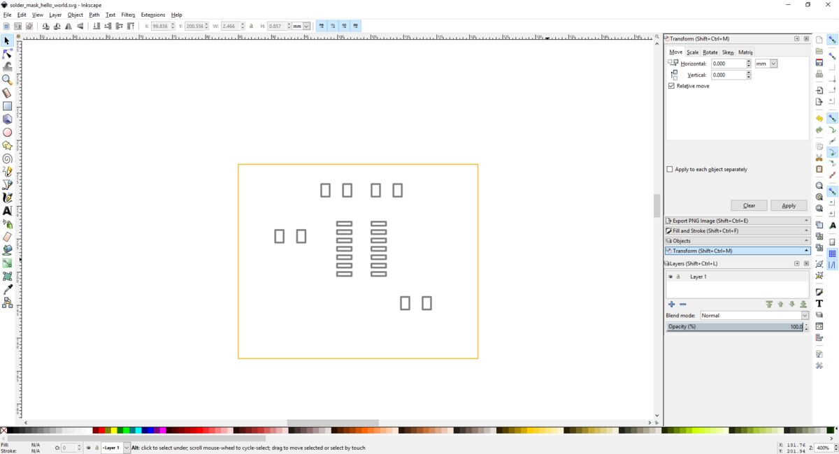
Import the PDF in Inkscape and check if everything worked alright (check the length of the board). Save as a svg
The svg file then can be cut with the laser cutter. We used thick paper with 240 grams per square meter. We tested around and found that a power of 10% at a speed of 100% is perfect to cut this paper. If you have you should use thinner paper (120gsm should be fine), because with this you get a lot of solder paste on the pads.
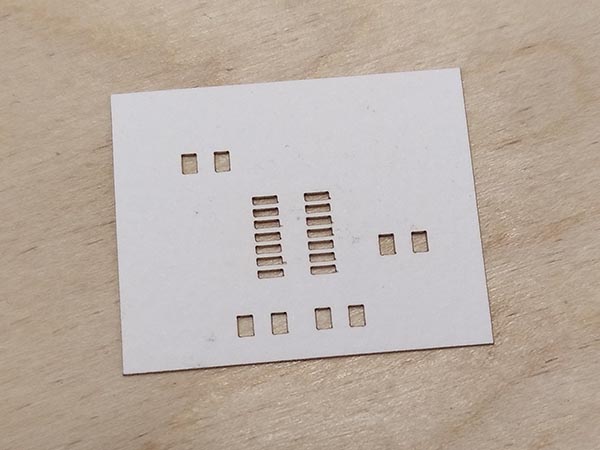
The finished stencil
Applying solder paste
Applying the solder paste is straightforward and shown in the following image series. Be careful to align the stencil, otherwise you can have solder paste on wrong positions. To put the paste on the board, put some paste on one contact and spread it over the mask to the next hole. I used a defect board from the garbage to spread the solder paste because it contains lead, so it is special garbage.
Hold the PCB in place with double-sided tape (remove before heating)
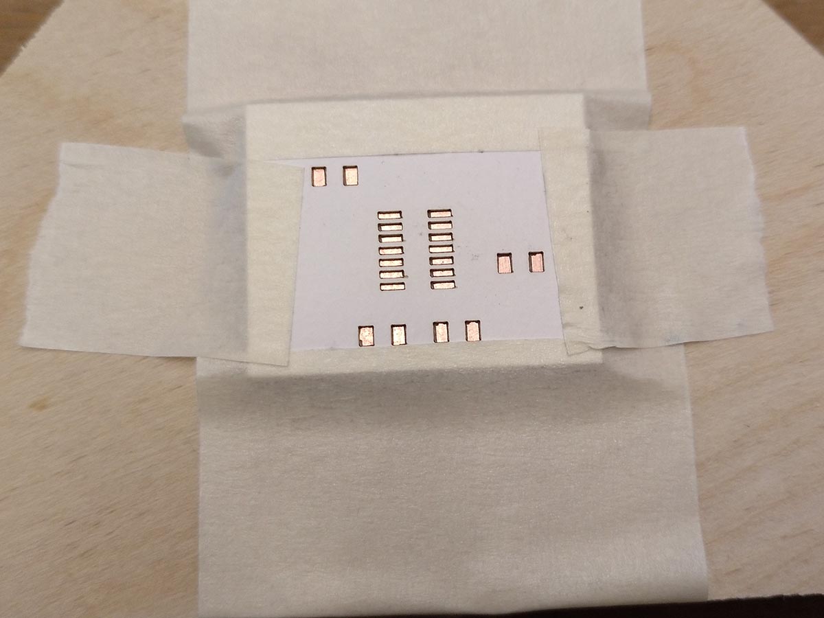
Place the stencil on top and hold it in place with some tape
Apply the solder paste
The board with solder paste
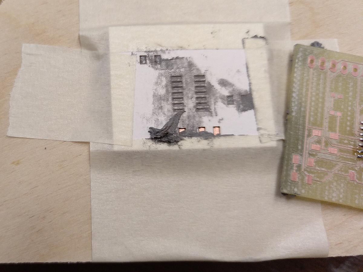
From the side you can see how much paste is on there
Placing the parts
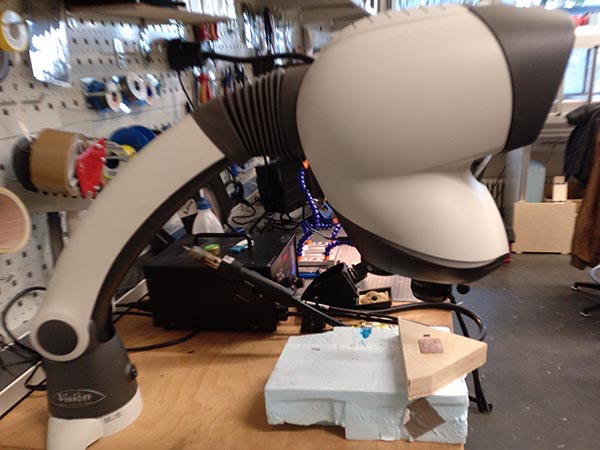
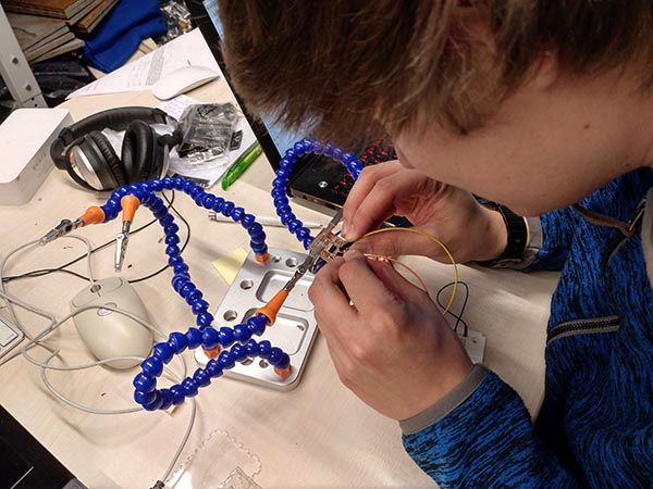
To place the parts I used a small tweezer. Placing the resistors and capacitors I straightforward, but for the attiny I used the stereomicroscope in our lab. This is awesome because you can really see in three dimensions! With this placing is just a question of a steady hand
Placing the resistors
Placing the ATTiny
The placed components
Soldering
This time the soldering was way better. The SMD components were no work at all. Just turn the hot air gun on and move it over the board until all joints are soldered. Also the through hole components were easily soldered, it was way better than the last time I soldered stuff.
We used a hot air gun to solder the components
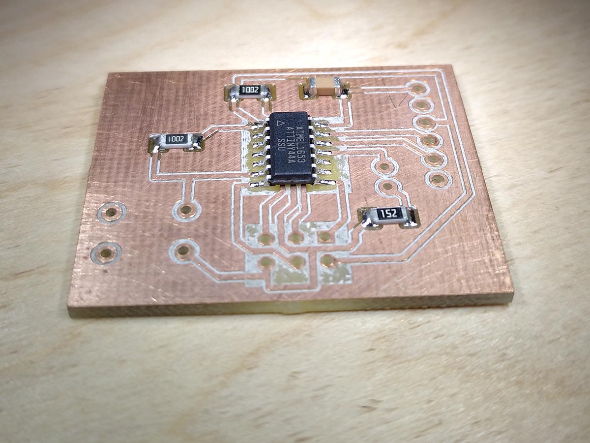
The soldered SMD parts
Holding the through hole components on a board
Soldered one pin of all components to hold them in place
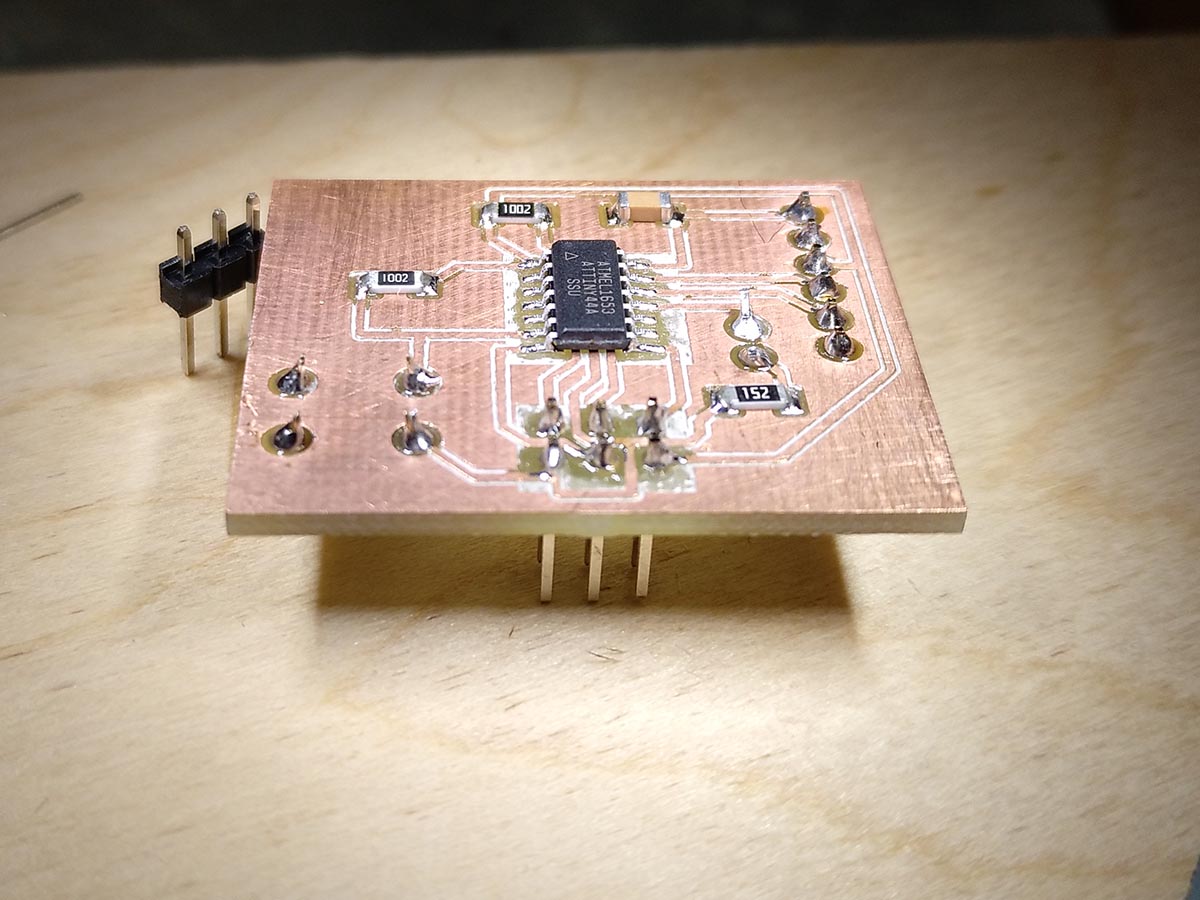
The finished board
The front side
Testing connections
To test the connections I first used a multimeter to see that nothing was unintentionally soldered together and that all attiny legs had a proper connection to the board. Then I used the stereo microscope to look at the solder joints, which all looked pretty good.
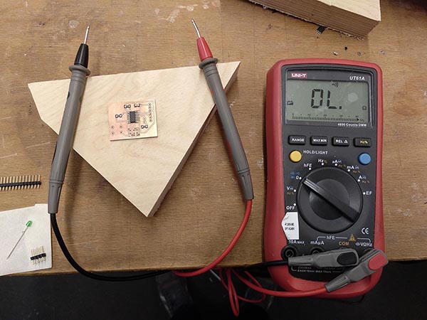
Testing connections
Programming and bricking the board
Prerequisites
Let's start with the setup for programming under windows. In the electronics production week, I already explained the setup with windows subsystem or linux, which doesn't work with the usbtiny as the wsl doesn't support generic usb devices. So you need to set everything up in your native windows, starting point for me was Brians tutorial:
                - Download the AVR Toolchain for Windows from the microchip website and install it by unzipping it to some folder (e.g C:/tools) and add this folder to your path


                - I didn't install GNU make, instead I already had installed MSYS with MinGW, which you can download here. This is a complete set of the standard linux binaries, available under windows. Quite handy if you want to be able to program under windows. But the make command then is named mingw32-make.


                - The last thing to install is AVRdude, version 6.3 for mingw. Also unzip it and add the folder to your path.
                - If you haven't already installed the drivers for your USBtiny you need to install Zadig and install the libusb-win32 driver for your USBtiny.
Programming
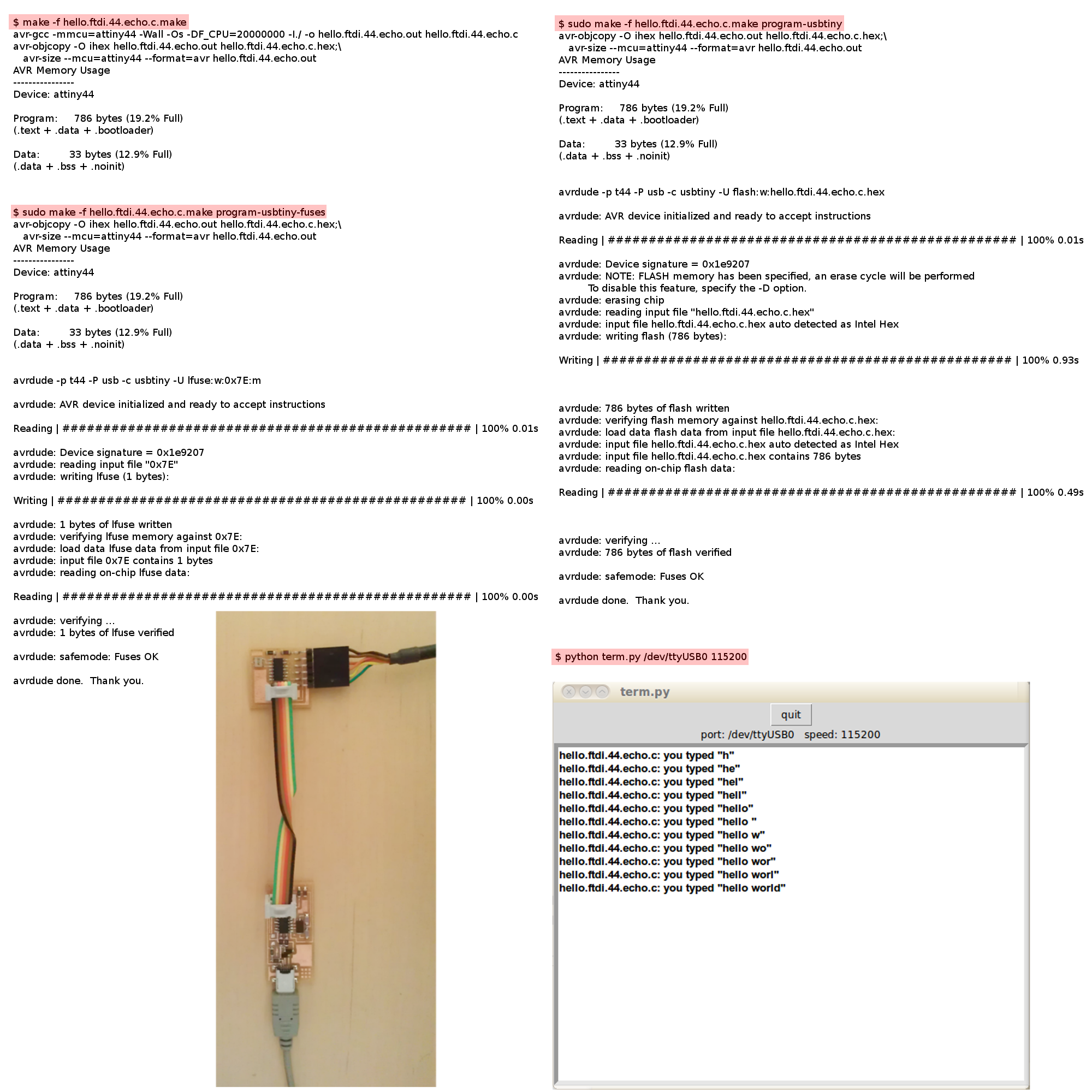
There was not much information on how to program this board. Actually, all the information was given in this image from the embedded programming page. It stated to execute:
Do not execute this! It will brick your board if you have no quartz on it! Read on to find more about the background
make -f hello.ftdi.44.echo.c.make
    make -f hello.ftdi.44.echo.c.make program-usbtiny-fuses
    make -f hello.ftdi.44.echo.c.make program-usbtiny
I executed the first two commands, with no error messages, which was fine. But then the command gave back: avrdude.exe: initialization failed, rc=-1. This means that your programmer is not connected to any board that can program. And this is because I executed the make ...-fuses command, which sets the fuse of the ATTiny to use an external oscillator as clock. As this oscillator doesn't exist, the board wouldn't boot anymore.
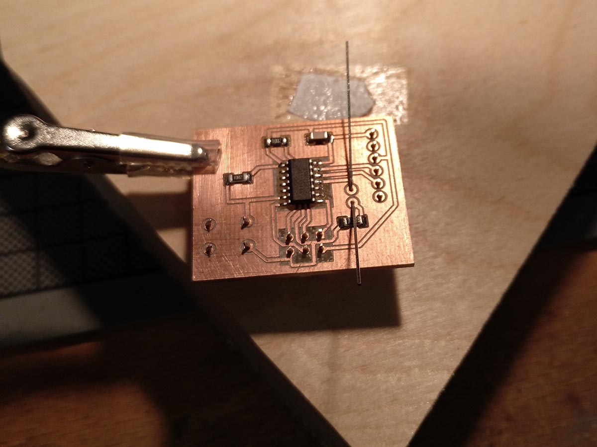
Reviving the bricked board
What happened?
To find the last information above, I had to dig through quite some places. First I looked up what the command in the makefile (avrdude -p t44 -P usb -c usbtiny -U lfuse:w:0x5E:m) does in the AVRdude manual. It sets the low fuse to 5E. After trying to get all the information from the attiny44 manual I found the fuse calculator where you can input your microcontroller and the fuse setting and get what that means: External Crystal Oscillator, Frequency 8-Mhz. With this information, I could also find it in the attiny44 manual. So my attiny didn't want to boot anymore because there was no clock signal.
Reviving
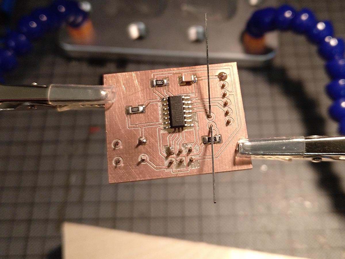
To get it back to life again I found information on this german webpage which states you can revive it when you just put a clock signal to the XTAL1 pin. The setup for getting a clock using a quartz can be found in the attiny44 manual on page 27. You connect both pins of a quartz to the attiny and use two capacitors of the same size (12-22pF).
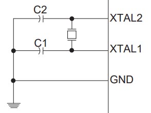
The schematic for unbricking from the attiny44 manual
I took two capacitors of the size 22pF and built the circuit on a breadboard.
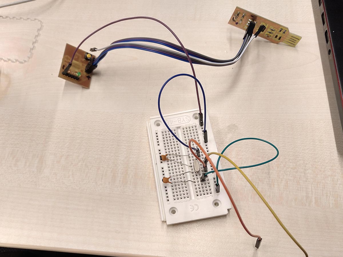
The setup for unbricking
As the XTAL1 and XTAL2 pins of the attiny were not connected to anything I had to hold the pins of the connector cables to the legs of the attiny. Somebody else needs to press enter to reset the fuse with the following command:
avrdude -p t44 -P usb -c usbtiny -U lfuse:w:0x62:m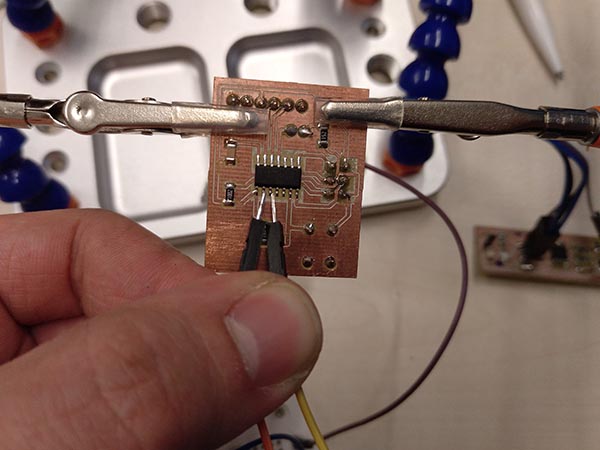
Connect the quartz to the XTAL1 and XTAL2 pin
Hold it there while the fuse is reset
This worked on the first try without problems. Now the board can be used again. You can now program it with the
make -f hello.ftdi.44.echo.c.make program-usbtiny command to program it with the echo hello-world program. But change the line with the cpu frequency F_CPU in the makefile from 20000000 to 8000000 as we don't use the external clock with 20Mhz, but the internal with 8Mhz.
Testing
I did flash the attiny with a led blinking program, which you can find in the embedded programming assignment, to test if it really was working. And I could see that I was able to bring the attiny back to life!
For the group project, we furthermore tested this board with a slightly different program.
Files
Here you can download the files created during this week:
Eagle project file
Eagle schematics
Eagle board design
Solder mask for the laser cutter