Week 04: Electronic Design
Printed circuit board (PCB) milling is the process of removing areas of copper from a sheet of printed circuit board material to recreate the pads, signal traces and structures according to patterns from a digital circuit board plan known as a layout file.
This week, we are making a USBISP(in-circuit serial programming), a device that allows program to be uploaded onto a microcontroller from a computer.
Group Assignment
We went through the process of making a FABISP from milling to soldering. From that, we were able to characterize the design rules for our own PCB production process. In the Individual Assignment part, I will explain the milling and soldering process in futher detail.
We will be using the FABISP circuit design files provided by Brian for the assignment. First, these circuit needs to be milled from a copper plate on a milling machine. Beside milling, photolithography is also another way of creating circuit boards. It is, however, a toxic process.
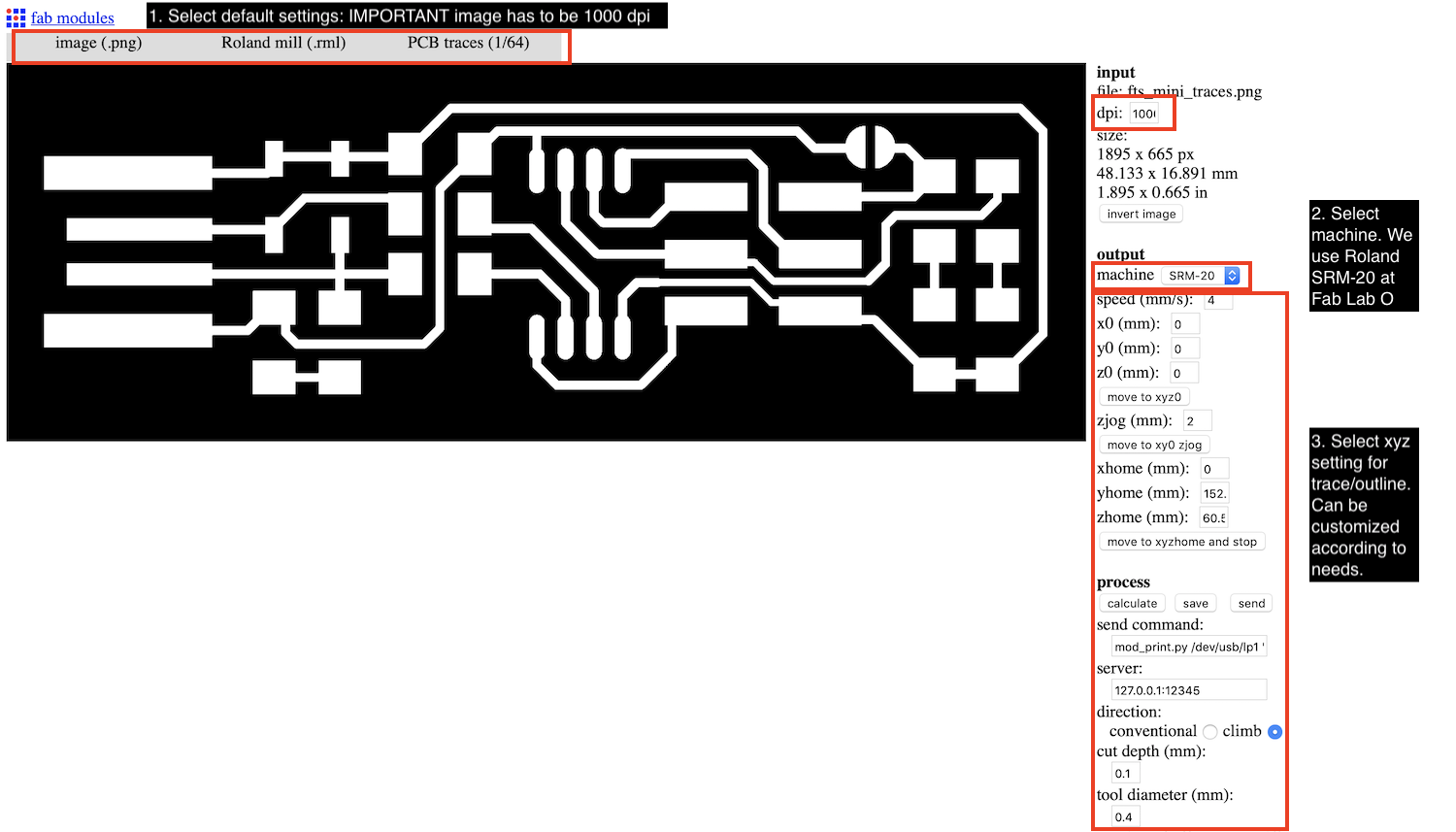
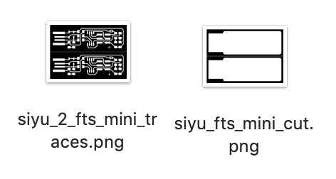
The files Brian provided are in 1000 pixel .png image format, which can be converted into tool path for the milling in Fab Module, an online software designed by Neil that allows to run machines in Fab Labs. There are two files that are required for circuit board milling, a trace file and an outline file. A trace is the engraved circuits. An outline cuts out the shape of the board.
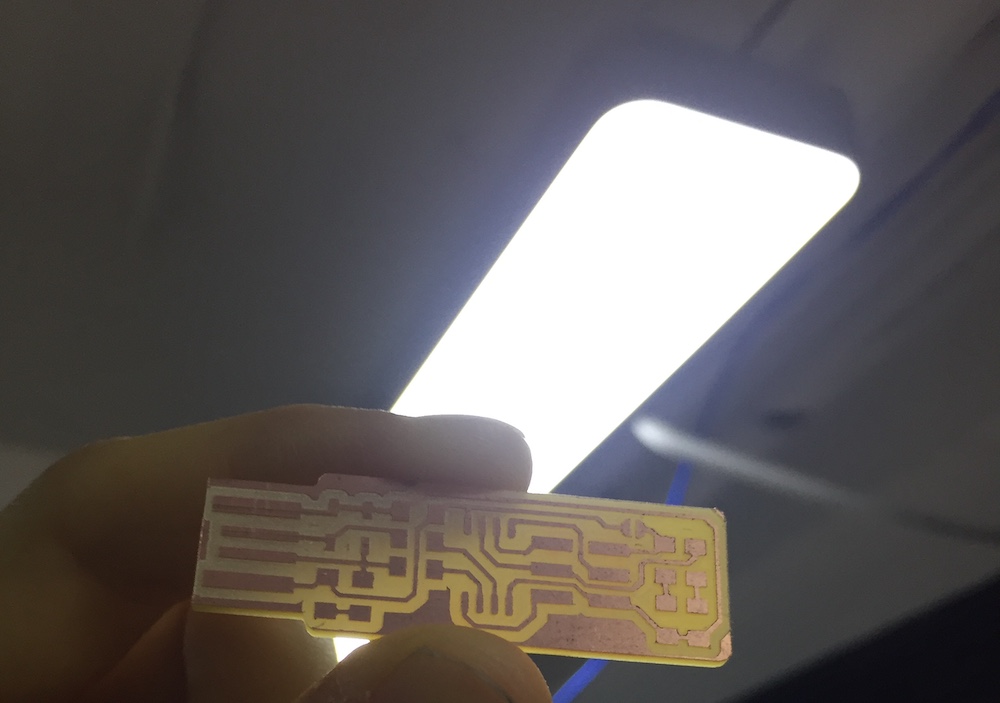
After the path files are generated, the files are sent to the milling machine to be milled. You can check whether all the traces are milled when holding it against a bright light.
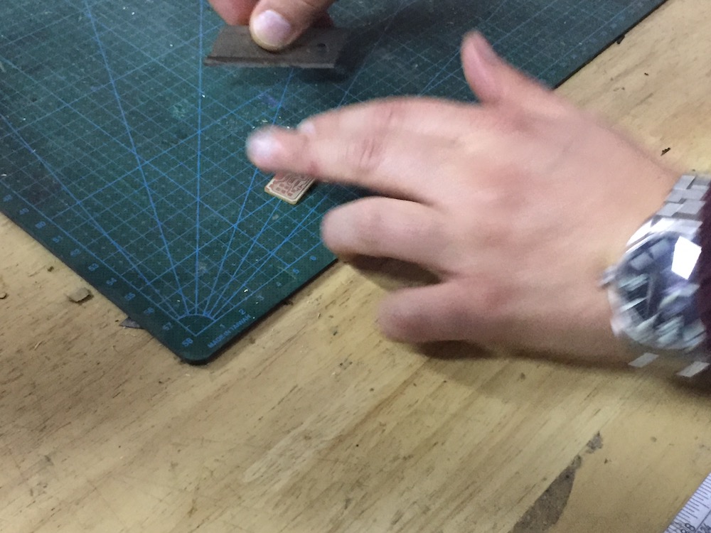
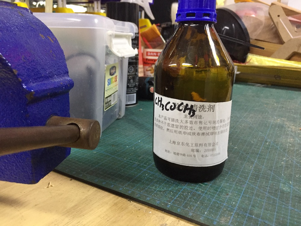
With the side of a sharp knife, gently go over the surface of the board to remove some of the rough edges. A sand paper can also be used, but can be quite aggressive and remove too much of the copper. Then, use a brush to apply acetone to the board for removing finger print and dirt.
The board is now ready to be soldered. First, touch the solder area on the copper with the iron until it heats up. Then, put a bit of tin wire onto the copper. NOTE: do not put a lot of tin at this point, since it is only used not to adhere the component with the board temporarily. Use a tweezer to hold one end of the component, while adhere the other end of the component with the ready-soldered tin wire. Then, add solder to both end of the component. Make sure to give enough time to let BOTH the tin wire and the component to heat up. A more detailed description on soldering can be found in the section below.

Individual Assignment
Prepare for milling
Prepare the black and white high resolution .png image files for trace and cut. This is an image, generated by an electronic design software, is needed to mill the board. On top of his file, I added my graphic signature (note: the size of the graphic has to be larger than the size of the endmill, which is 0.4mm).
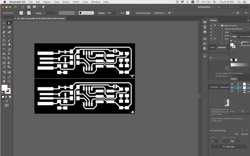
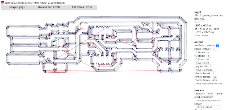
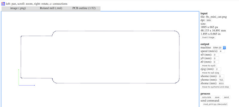
To generate toolpath for the milling machine, I have used Fab Modules, a software developed by MIT that helps you to use machines in fab lab by creating movements for the machines. I used it to create the movement for the Roland Miller at Fab Lab O based on the .png image for traces and outlines.
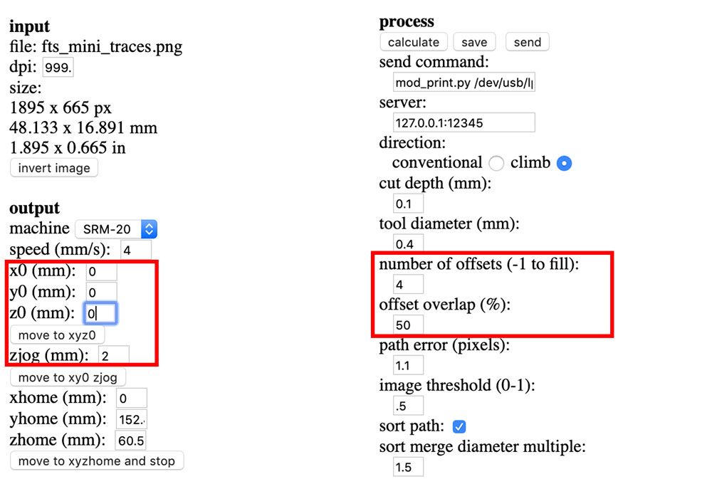
Import the .png image in Fab Modules and select the right settings. Afterwards, click on “Calculate” to generate the toolpath and ''Save'' the result as a RML format file
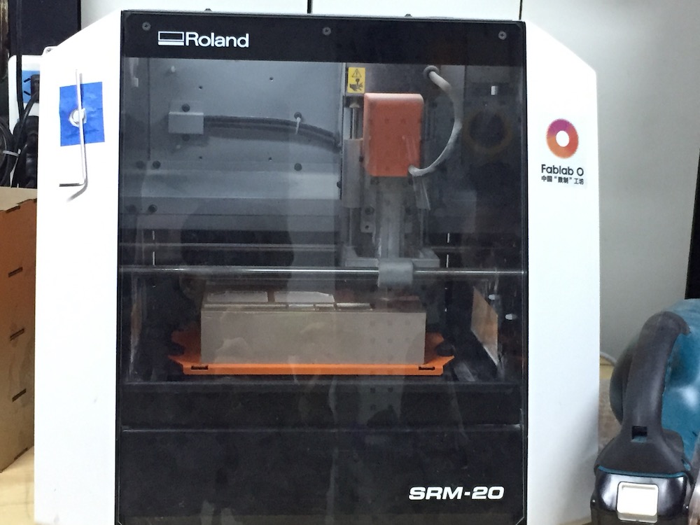
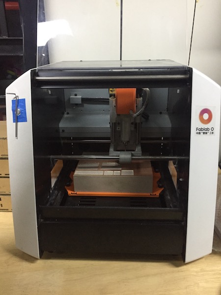
Milling on Roland SRM-20
Material for milling comes in different fire resistance (fr):Copper has a fr of 1 that is not high in resistance but east to cut with the milling machine; Fibre glass has a fr of 4 that is high in resistance and hard to break but not suitable for milling. For our purpose, we used a laminate sheet with a very thin layer of copper.
Material is placed onto the bed of the machine with double-sided tape. MAKE SURE to buy a double-sided tape that can be peeled off completely from the board without leaving any adhesive! The surface of the material MUST be parallel to the x and y-axis of the machine.
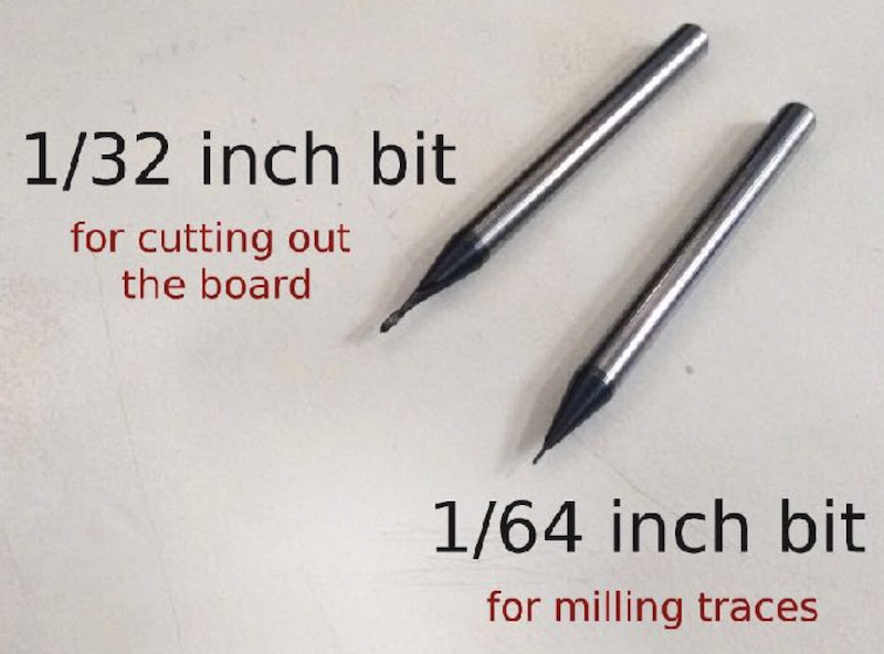
Endmill is the cutting tool of the milling machine. We used a 0.4mm endmill to engrave the traces on the material surface and a 0.8mm endmill to cut through the material. Endmill moves in x, y and z-axis on the machine. Z-axis must remain up all time when moving across x and y axis, or else the tip of the endmill might touch the material bed and break.
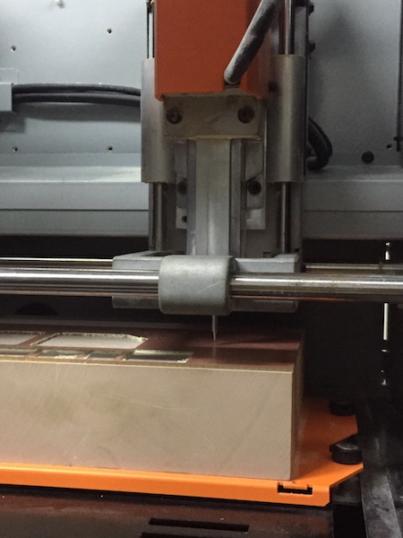
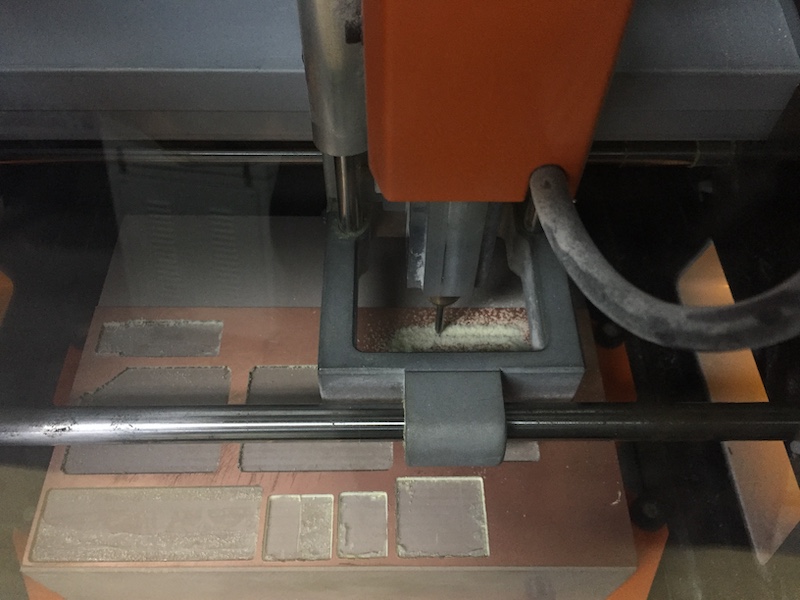
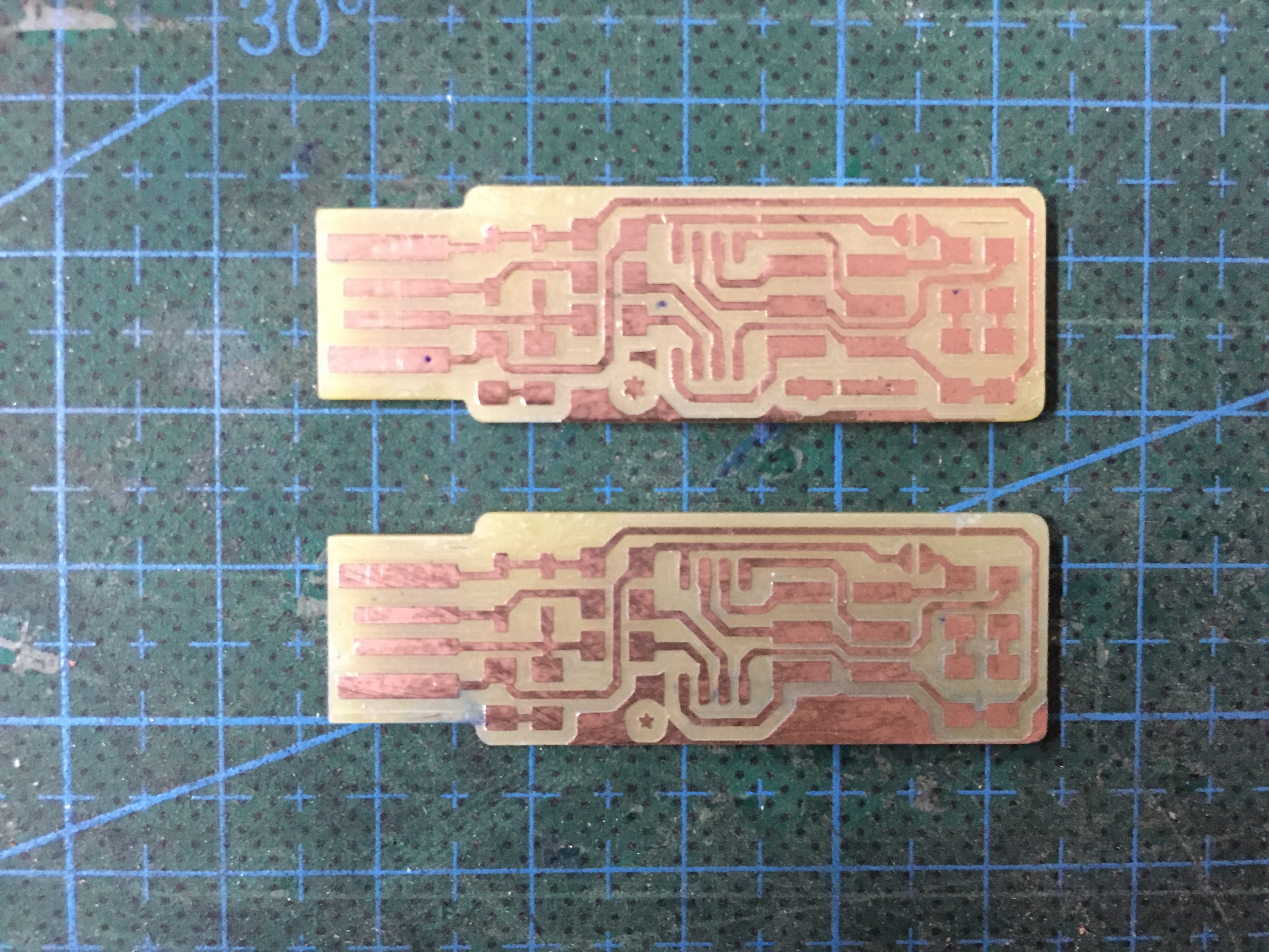
We did the traces engraving first, and then the outline cutting.
To start milling, first make sure the endmill is at the origin position on the board that you need. NOTE: The cut starts at the left corner of the image. Through the software V-Panel for SRM-0, the position of the mill can be altered. First, take the origin position of z by moving the endmill to the center of the material. Then, unscrew the endmill by holding its tip with one hand, while releasing the screw with the other hand. After the screw loosens, slowly let the tip of the endmill touch the material surface. Take z origin by clicking on Z under Set Origin Point. Then, move the z position upwards for moving the mill to set it x and y origin (Click on X/Y under Set Origin Point).
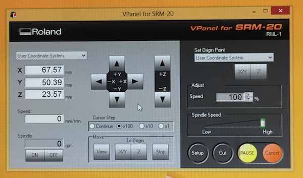
Click on Cut to output the file to the miller. You are all set!
Remove the material from the material bed slowly with a palette knife. Then remove the double-sided tape on the back of the material.
With a brush, gently clean the surface of the material with acetone to remove finger prints.
Soldering
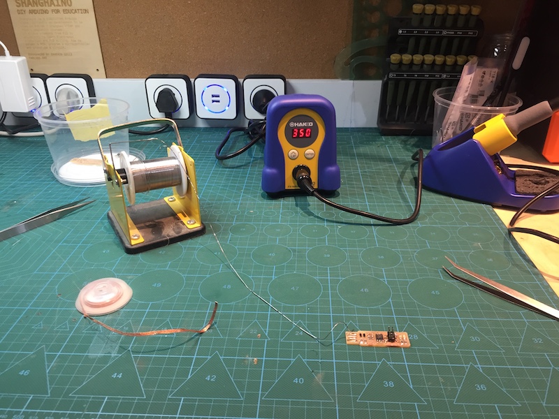
To set up for soldering, make sure you have a good light source. The light we use at Fab Lab O comes with a magnifier, which help with checking whether components have been soldered properly. Turn on the soldering machine and make sure it is at 360 degree celsius.
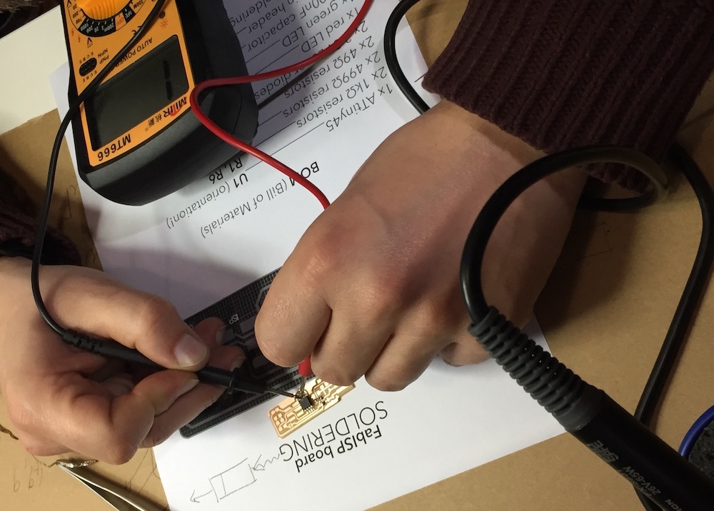
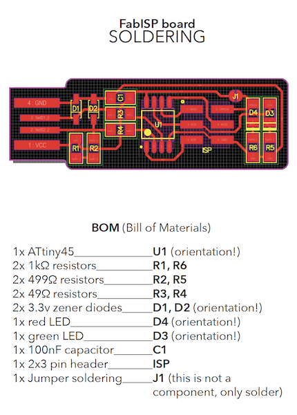
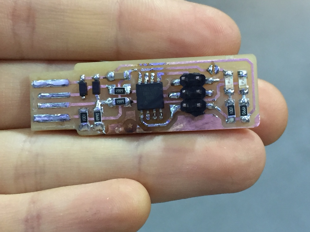
The components I will be using are found on the FABISP board chart. Make sure all the components are facing the right side when soldered. The most critical ones are the ATtiny, zener diodes and the LEDs.
I started from soldering the center component (U1) and then made my way out. Here is the step I followed to solder a component onto the board:
1. Make a small dot of soldering wire on the right position for one end of the component.
2. With a twisor, hold one end of the component, while using the tip of the soldering iron to melt the soldered dot.
3. To warm up the surface, lightly press the tip of the soldering iron on the other side of the component.
4. With one hand holding the soldering wire and another hand holding the soldering iron, solder the other end of the component.
5. Make sure each end of the component sits flat on the board and is covered in solder. If needed, add more solder on each end.
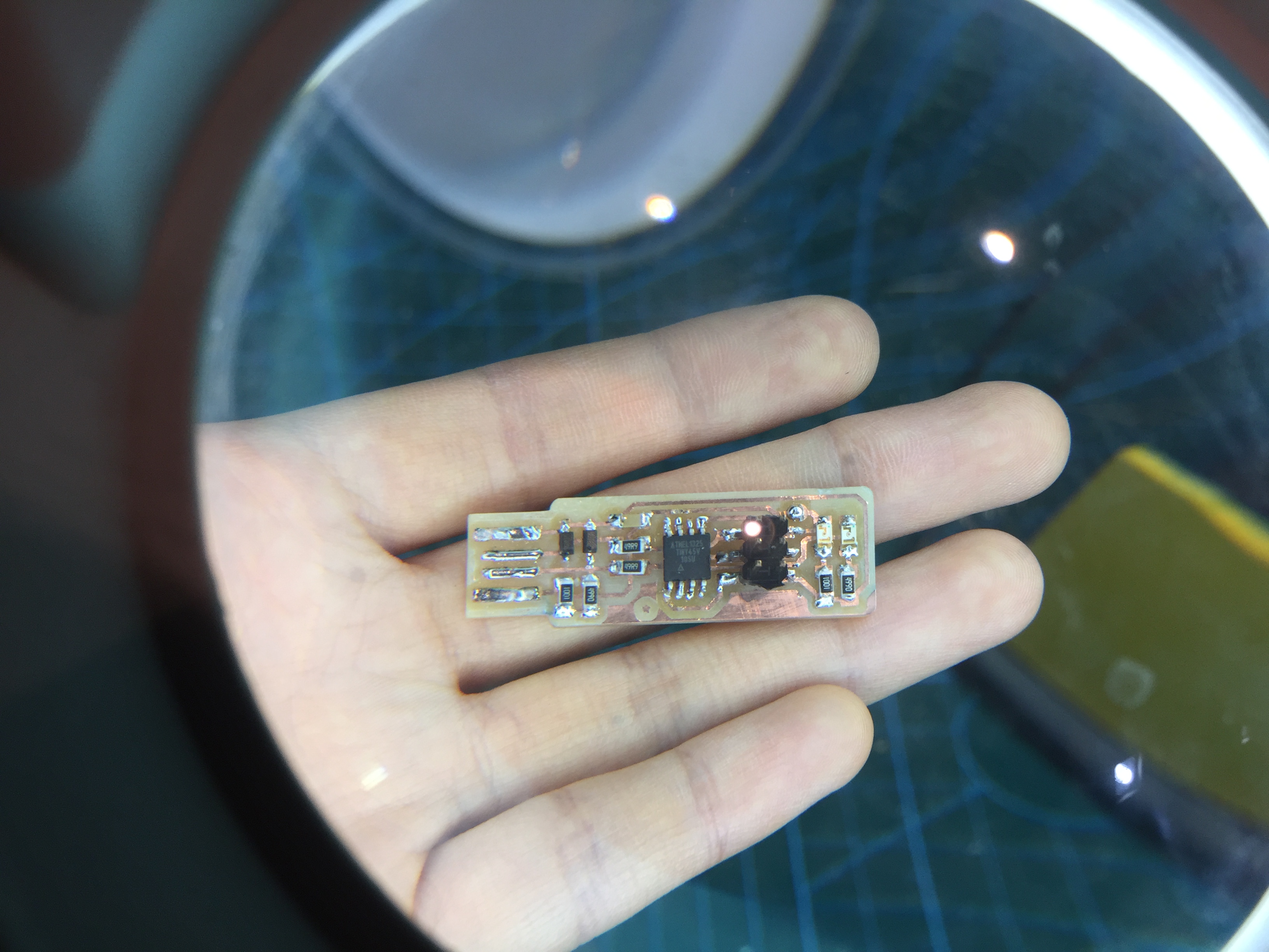
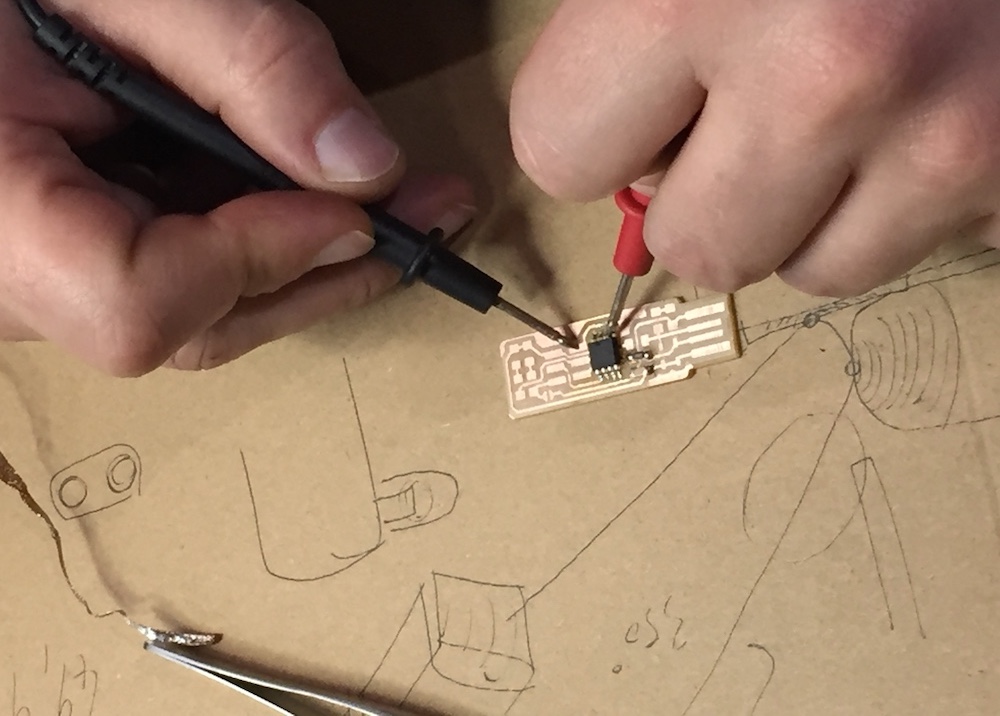
To check whether the parts are soldered properly, use a multimeter and test the connections between each component by looking at the FABISP board chart.
Programming
First, make sure Xcode + Crosspack AVR (for Mac) are installed. Then, download the firmware for the AtTiny45 FabISP. NOTE: a working FabISP is needed for programming a new FabISP.
In terminal, make sure it is in the folder of the firmware (e.g. cd user/desktop/fts_firmware_bdm_v1)
Then, connect the boards properly:
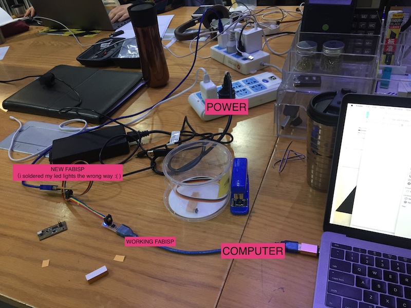
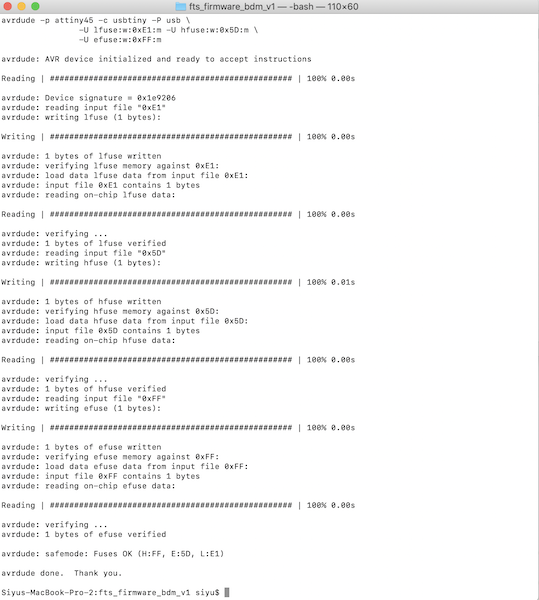
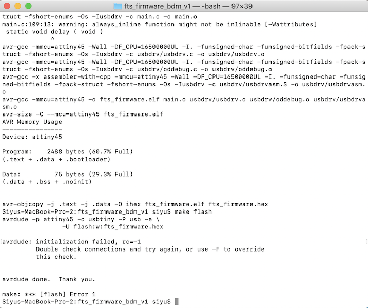
Run the commands in order: 1) make (a file named fts_firmware.hex is created in the folder) 2)make flash 3)make fuses

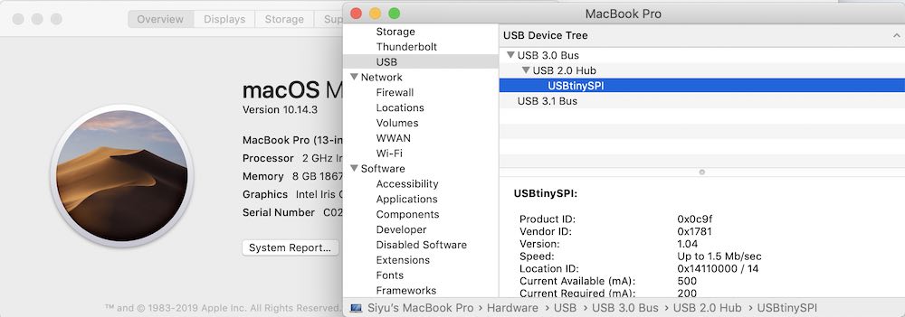
Make sure the fabisp is correctly recognized by the computer. On Mac, the USB port connection can be checked under Finder/About This Mac/System Report:
At last, run make rstdisbl
Remove the bridge on the older jumber using the soldering iron and the new FabISP is ready to program other boards!
De-bugging
It is likely the new FabISP would fail at make flash command.
When this occurred, there are several solutions:
1) Reconnect the FabISP
2) Try to connect the FabISP on another computer
3) Clean the FabISP with alcohol using a toothbrush
4) Check whether the components have enough solder
5) Check the connections between the components with a multimeter
6) Remove the current ATtiny (the ''brain'' of the ISP) and solder a new one