The Printed Circuit Board is mechanically
supports and electrically connects electronic components or electrical
components using conductive tracks, pads and other features etched
from one or more sheet layers of copper laminated onto and/or between
sheet layers of a non-conductive substrate. The Components are
generally soldered onto the PCB to both electrically connect and
mechanically fasten them to it.
I am learning to do some basic electronics production, specifically
creation of a PCB by milling, then adding the components and finally
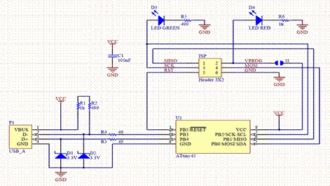
burning the code to it. I’ve made an in-circuit programmer
(FabISP) by milling the PCB. The FabISP is an in-system programmer for
AVR microcontrollers designed for production within a FabLab. It
allows us to program the microcontrollers on other boards which we
make during our upcoming assignments. Currently I’ve chosen the
FabTinyISP Minimal version - this uses ATtiny45.
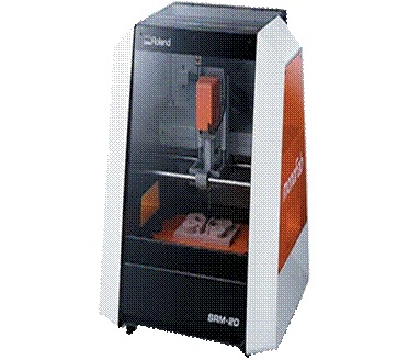
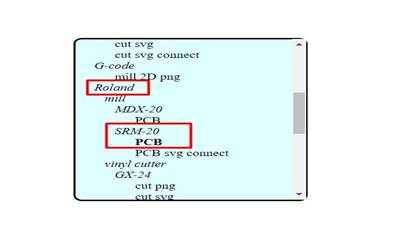
We have two PCB Milling Machines - Modella MDX-20 and Roland monoFab
SRM-20. I’ve used Roland monoFab SRM-20 for making my fabTinyisp
board. By observing on Roland site, I’ve understood that SRM-20 is
Roland's latest generation 3D desktop milling machine, incorporating
innovative subtractive rapid prototyping (SRP) features to deliver
accuracy, smooth finishes and efficiency in a compact format.
| Model |
SRM-20 |
| Cuttable Material |
Modeling Wax, Chemical Wood, Foam, Acrylic, Poly acetate,
ABS, PC board |
| X, Y, and Z Operation Strokes |
203.2 (X) x 152.4 (Y) x 60.5 (Z) mm |
| Work piece table size |
232.2 (X) x 156.6 (Y) mm |
| Distance From Colet Tip to Table |
Max, 130.75mm (5.15 in) |
| Loadable Work piece Weight |
2 kg (4.4 lb) |
| Control Command Sets |
RML-1, NC code |
| External Dimensions |
451.0 (W) x 426.6 (D) x 426.2 (H) mm |
| Weight |
19.6 kg (43.2 lb) |
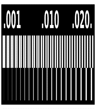
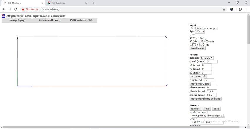
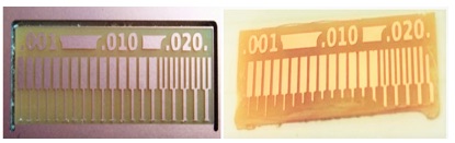
Group Assignment: We characterized
the design rules for our PCB production process. Line Test:
Manoj Sahukar and I teamed up for the assignment.
A. The line test images were taken from
Fab
Academy Electronics Syllabus.
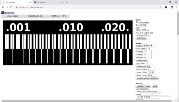
B. We used
FabModules to generate
.rml files. Various other settings like process, speed, X, Y and Z
coordinates were entered.
C. There was 1 line of a Rectangle Red which showed the jog path. The
fab module did not create a close rectangle as can be seen form the
picture above.
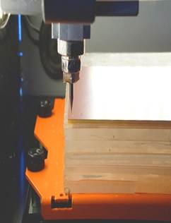
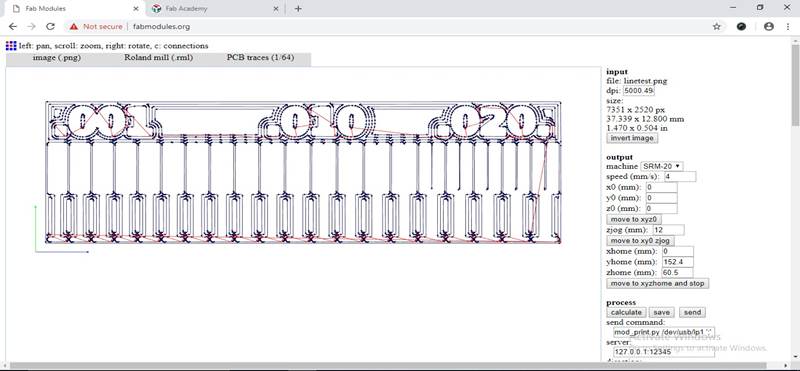
D. We cut the board on SRM 20 machine, gave 2 commands to trace the
lines of the various thicknesses and cut the outline.
The line tool path looks as shown below.
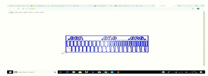
The saved .rml image and after milling looks like this.
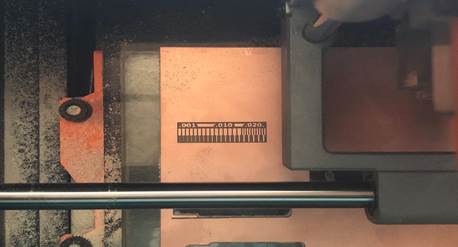
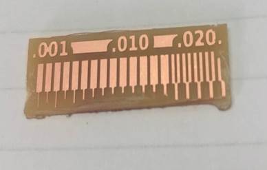
The board showed the smallest thickness line when it was cut properly,
thus giving the green signal for the tracing and outline ahead.
We cut the board with the grinding machine as it was not cut from one
side properly. Though this damaged the board, yet, the objective of
the assigment was achieved.
We cut the board with the grinding machine as it was not cut from one
side properly. Though this damaged the board, yet, the objective of
the assigment was achieved.
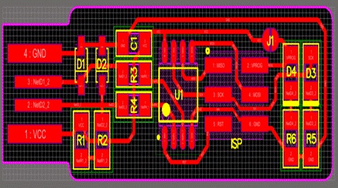
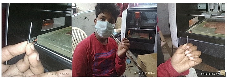
Individual Assignment – I made an in-circuit
programmer by milling the PCB, using SRM 20 and programmed it. Prof.
Neil introduced various ways to make our 'Fabisp'. Sean, Alex, Tomás,
Jonathan, Brian & Zaerc have worked using ATtiny45 and Ali,
Valentin, Bas, Andy & David used Attiny44. I choose the Brian's
Board to mill my PCB. So i downloaded the '.PNG' file of "Board
traces" and "Outline".
PCB Setup – The PCB Board of a suitable size should
be fixed on the sacrificial layer using the double sided tape. Care
should be taken to evenly place the board. Any variation may cause
breaking the tool. If the milling surface is not on level, then need
to apply pressure gently on the raised areas. In case it does not
work, redo the adhesive part.
Make sure that the level is distributed uniformly.
PCB Milling – I have used a Router for Milling the
PCB. The tools used are
SVP Laser
CNC Router
Single Sided Copper clad Circuit PCB Board
FR1 double sided Tape
Engraving Bits
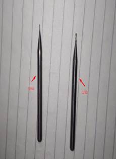
Attaching the Milling Bit – The Milling Head has to
raise by using the “Tool Up” button on the Modella Control Panel.
Using the Allen Key, gently loosen the Hex Nut on the Rotating part on
the Milling Head. Then gently remove the existing Bit. Depending on
the type of cut, Select from the two available Bits – 1/64 for Traces
and 1/32 for Border Cuts.
While storing the bits, ensure that they should be placed in its
appropriate container cap on. It is also a good idea to place a sponge
or a soft cloth beneath the tool holder to ensure that the bit is not
damaged in case it falls while removing it from its container. In my
assignment, I have shifted the origin to 2.78 to mill on the space
available at the top left corner.
Then moved the Bit down by using the “Tool Down” button in the front
panel, till about 0.5 cms above the milling surface.
Finally used the Allen Key to loosen the Hex Nut holding the bit
firmly so that it drops on the milling surface perfectly and fastened
the Nut.
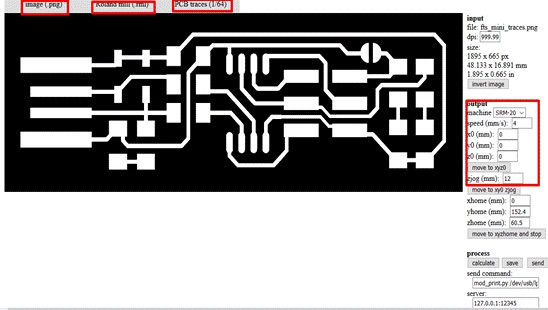
The board layout needs to be available as an image .png file in black
and white colour.
The black portion is removed by the miller and the white portion
remains as the circuit trace as shown below.
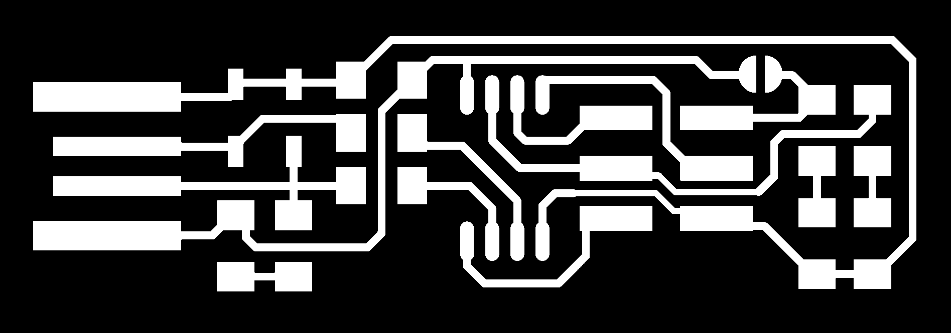

I have used Brain example as reference follwed as under –
http://fab.cba.mit.edu/classes/863.16/doc/projects/ftsmin/index.html
Files from Brian: “Ttaces and “Outline Cut” files in
PNG format of 1000 dpi were downloaded from Brian.
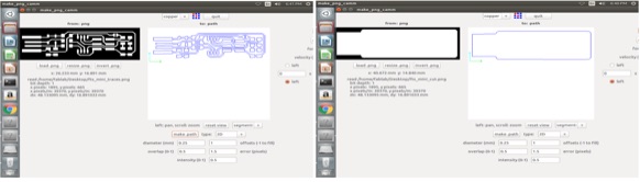
Fab Modules : I have used the Gab Modules to change
the settings and format the png.file as under –
The process to convert images using FAB module -
1.Go to the online fab module.
2.Import image, set SRM-20 machine.
3. Make X,Y,Z to zero and Zjog-12.
4.Then calculate; then png image will be converted into .rml and we
can see it’s traces.
5.Download the .rml image and share to the Vpanel.
Procedure I have followed -
Input File – selected the image .png format as the
file is in this format.
Output File – Roland Mill .rml is the desired format
of the output file as it is supported by SRM-20.
Process – For engraving and traces, I have selected
PCB traces 1/64. For cutting PCB Outline 1/32.
Machine – I have used the SRM-20 milling machine for
Milling.
X,Y,Z axis – all the 3 values were adjusted to 0mm.
Fan Speed – 4mm/s for both the processes – Traces and
Outline.
Zjog- 12mm is the safe distance when the end mill
moves to mill from one part of the design to the other.
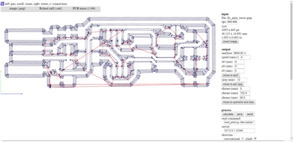
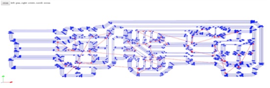
The rml trace is shown below -
 Calculate –
 Shows the path of the end mill in red
lines on the file design.
 Save –
 I have saved the file in .rml format and it
is now ready for milling.
Setting the Origin – The origin has to be set to
enable the machine start the operation, which is vital in order to
select the desired area on the copper board on which I have to mill
the pcb.
First, select the “move to xmin, ymin” option. This would move the
milling head to 0 (20, 20) by default. Then I have changed the values
to locate the desired area.
Calculate – Shows the path of the end mill in red lines on the file
design as seen here under.
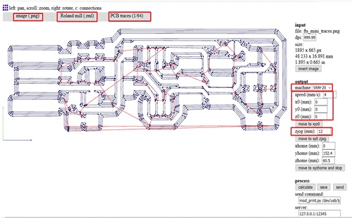
Save – I have saved the file in .rml format and it is now ready for
milling.
Setting the Origin – The origin has to be set to enable the machine
start the operation, which is vital in order to select the desired
area on the copper board on which I have to mill the pcb. First,
select the “move to xmin, ymin” option. This would move the milling
head to 0 (20, 20) by default. Then I have changed the values to
locate the desired area.
This is the rml file trace - A5 Electronics
Production_files\fts_mini_traces
(2).rml
This is rml file cut - A5 Electronics
Production_files\fts_mini_cut
(2).rml
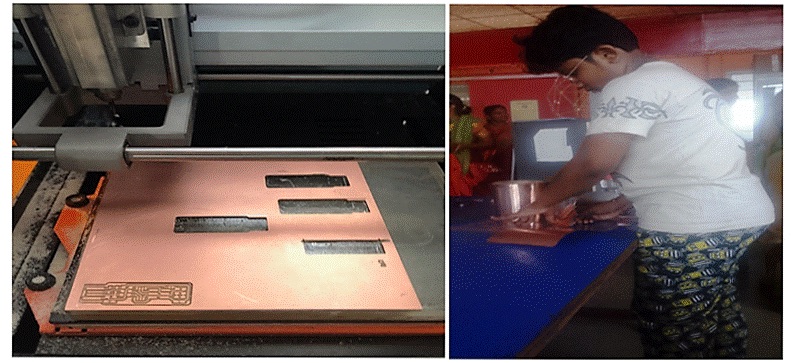
Milling the Board – I selected the PCB Traces option
under the Process Drop Down Menu. Then adjusted the cut depth to
0.1mm, which mills the copper.Selected the Calculate Option to
generate the tool path for the device. Went to the Tool Path and saw
if all the traces were available. It was interesting to note that if
we give 1 as the offset value, then all the copper, except the traces
will be removed. Lastly, clicked the Send Button to send the tool path
to the device to start cutting. A status window is displayed showing
the elapsed time and remaining time. Mine too about 10 minitues to ill
the traces.
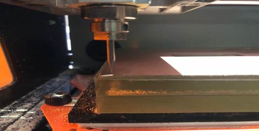
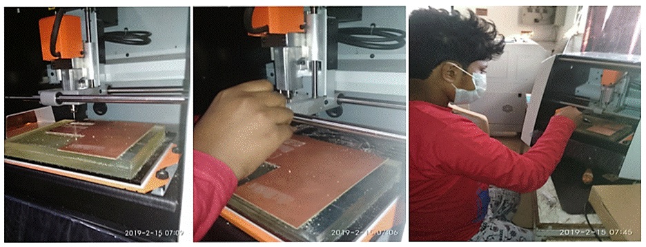
Sacrificial Layer – As the name suggests, it
sacrifices itself for saving the base plate from any damage, just in
case something goes wrong and the milling bit goes further than
expected, it might end up in damaging the base plate. The procedure is
to apply the dual sided tape onto the copper clad board which is about
the same or of a greater size to that of the plate which is going to
be milled. For cleaning and placing the sacrificial layer, I have used
Acetone to clean the surface. The width of the acrylic sacrificial
layer in our lab is a smooth and uniform surface, which vitally
decreases the chances of the bit getting damaged.
Sticking the FR1 board to the sacrificail layer – I stuck the double
sided tape on the bottom of the FR1 board and stickerd it on the
sacrificial layer.
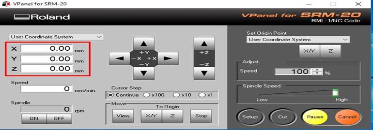
 V Panel Software and Machining –
This software gives
the access to set the origin and adjust the axis and give the command
to the machine.
Setting the X&Y axis – Under the User Coordinate
system and looking at the space on the FR1 board, the origin was set
up.
Adjusting the End Mill in the Collate – The End Mill
is inserted in the Collate and Moved to set the X, Y origin. I have
set collate loose and allowed the End Mill to touch the board.
 Setting the Z axis –
 After tightening collate, this
fixed position was marked as the origin for Z axis.
Set up and Tracing – Under the Set up Command, the
file was sent to the machine and it started tracing.
Operation – The end mill moved and traced the board.
The speed and spindle value was visible on the software.
 Changing the End Mill –
 The End Mill was changed from
1/64 to 1/32 for cutting the outline. I have followed the same
commands keeping the X, Y origin positions constant. The Z origin was
marked again because the position may slightly while changing the end
mill.
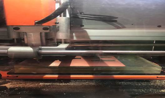
 Operation –
 This time to cut the board, the end mill
went deeper showing the value in the display. The machine stopped on
completing the instruction and then I removed the PCB from the sheet.
In case the task is not completed satisfactorily, then redo the traces
with a little more depth as I did.
Once the traces are ready, then replace the bit with the 1/32 bit and
repeat the same process with the border for cutting out. Be sure to
“cut out board” option in the process dropdown menu.
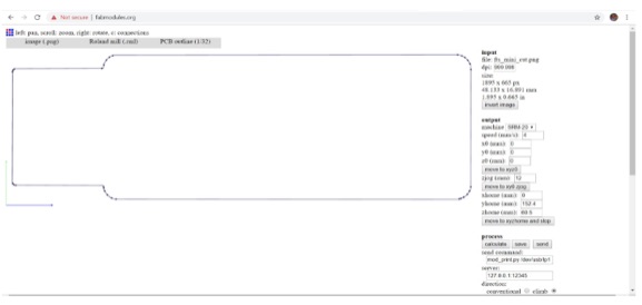
I have the .png file that looks like the one below for border cutting.
When the process is completed, then I have removed the cut board from
the mill.
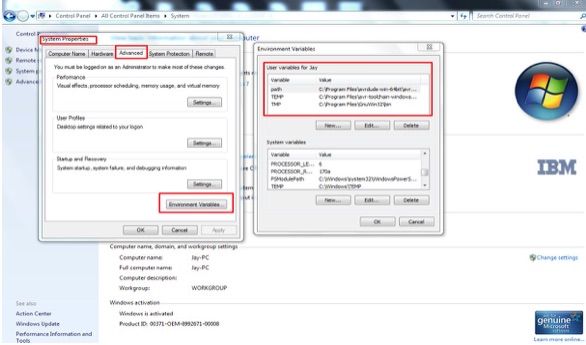
Under User variables, select "Path" and click the Edit button.
If you don't already have a variable called "Path", click the new
button to create it, enter "Path" without the name, and fill out the
value as described below.
C:\Program Files\avr8-gnu-toolchain\bin
C:\Program Files (x86)\GnuWin32\bin
C:\Program Files\avrdude
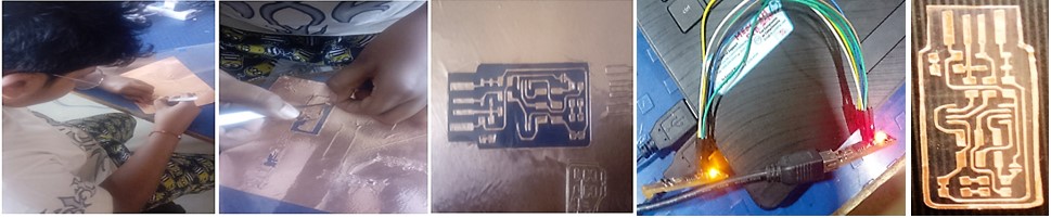
Stuffing -Once the board is milled the next task is
solder the board with the components. Stuffing means assembling the
parts on the board. First, the components are selected and marked on a
paper for clarity. Stuffing can be done by manual soldering using the
electronics workbench or by a more automated process using
pick-and-place and reflow oven.
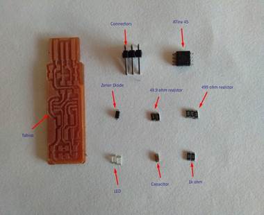
It is important to identify and note the orientation of the parts,
which go into the Board. It is suggested to palace them in a mark able
tray/sheet to solder them onto the board. The zener diodes are marked
both in and on the drawing and on the packages, with a little line on
the cathode side.
The LED cathodes on the PCB drawing are marked with dots and thicker
lines. The one in our lab has a green line visible on the cathode side
of the epoxy lens.
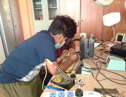
Soldering - Soldering is a process in which two or
more items are joined together by melting and putting a filler metal
into the joint, the filler metal having a lower melting point than the
adjoining metal. Unlike welding, soldering does not involve melting
the work pieces.
 Material Used for Soldering-
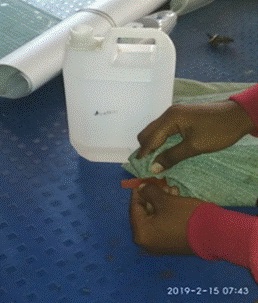
- Sand Paper – I scrubbed the PCB board with the sand paper. This
made the surface rough and easy for the filler to stay on the
board.
- Components of the Circuit – I have used the Fab Tiny ISP parts
as follows for my Brain Board.
1x ATTiny 45 / ATTiny 85
2x 1k / 2x 499 Resistors / 2x 49 Resistors
2x 3.3 v zener diodes
1x Red LED / 1x Green LED
1x 100nF Capacitor
1x 2*3 pin head
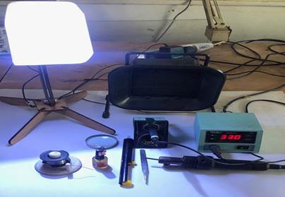
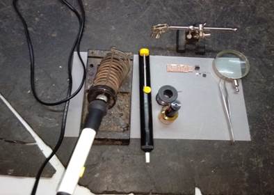
Equipment Used for Soldering –
Filler – Wired melted in contact with the soldering
iron and dried immediately the moment it is place on the PCB board
which fixes the board and components.
Flux – This chemical facilitated my soldering
process. I tried both liquid and solid. But I enjoy with the liquid
flux.
Soldering Iron Rod – I have used the soldering rod
@333C to melt the filler and place it between the components and the
board. Then placed back the iron rod in the stand.
Hot Air Gun - The hot air at a very temperature
melted the filler instantaneously. This tool was very handy during the
DE soldering.
Exhaust Fan – This exhaust fan pulls off the gases
released during melting the filler.
DE Solder Pump – The pump sucked the filler and
helped removing the components from the board. The Mr. Cleaner.
Tweezers – The tweezers were very helpful to pick
and place the components onto the board.
Magnifying Glass – The components are marked and the
words written on it are tiny. This tool helped me a lot in seeing the
board clearly.
Night Lamp – The light was useful in identifying the
small components of the circuit and find the gaps to solder.
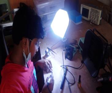
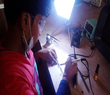
 Fixing and Handling –
 By looking at the diagram fro
Brain, I have placecd the above components using the equipment
soldered my PCB.
I faced an epic failure as it got damaged; but moved ahead to build
four more PCBs.
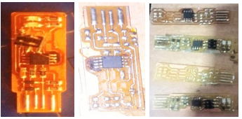
Then I have built another one and more. But the final built was a good
one, which works after it bork using for electronics design.
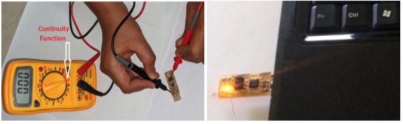
Testing – I have tested the soldered PCB’s using a
Digital Multimeter. The PCB test of a board will use capacitance and
resistance. The Capacitance test will test for opens and shorts by
sending a charge on the trace and then probe each net to measure the
induced capacity. The Resistance test measures resistance as the
current flows through a conductor/trace, in ohms. I have also checked
for the continuity between the soldered components and the traces by
using the continuity mode on multimeter and the LED is blinking wbhen
connected to the laptop as shown below.
 Programming –
 It is the process of taking an algorithm and encoding it into a notation, a programming language, so that it can be executed by a computer. Although many programming languages and many different types of computers exist, the important first step is the need to have the solution. I have followed this process
http://fab.cba.mit.edu/classes/863.16/doc/projects/ftsmin/windows_avr.html
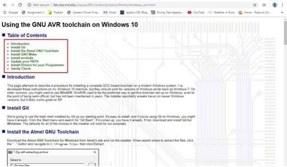
Later installed the Atmel GNU Toolchain from
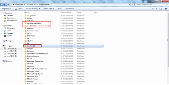
https://www.microchip.com/mplab/avr-support/avr-and-arm-toolchains-c-compilers and ran the installer. When asked where to extract the files, click the "..." button and navigate to C:\Program Files, then click Extract. I Download Gnu Make and launch the installer. Accept the default location for the installation.
I downloaded
Avrdude and extracted the zip file. Then extracted the file copy and pasted in 'C:\Program Files' and completed the Installation.
Later installed the Atmel GNU Toolchain from
https://www.microchip.com/mplab/avr-support/avr-and-arm-toolchains-c-compilers and ran the installer. When asked where to extract the files, click the "..." button and navigate to C:\Program Files, then click Extract. I Download Gnu Make and launch the installer. Accept the default location for the installation.
For updating the path I opened the Control Panel, then go to System, choose "Advanced System Settings". Under the Advanced tab, click the "Environment Variables" button. As I din't have a variable "Path", I clicked the New button to create it by entering the "Path" without the name. These three values were added as follows:
C:\Program Files\avr8-gnu-toolchain\bin
C:\Program Files (x86)\GnuWin32\bin
C:\Program Files\avrdude
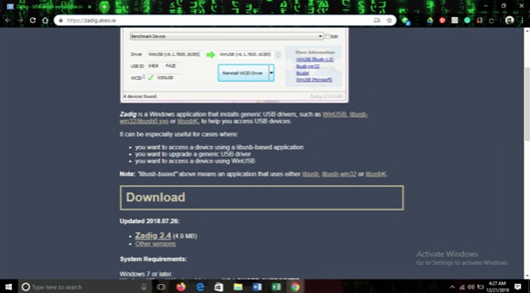
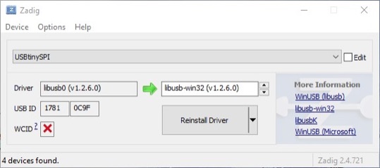
As per the assignment requirement, I programmed my FabISP board with Jaydip’s 'FabISP Programmer' using 'Zadig' software. Zadig is a Windows application that installs generic USB drivers. Then I downloaded Zadig and selected the "USBtinySPI" device from the list.
And selected
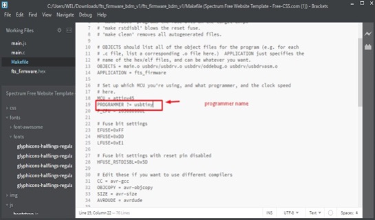
Before the Programming we need to edit "Makefile". But we need to set the programmer name like usbtiny and edited the Makefile.
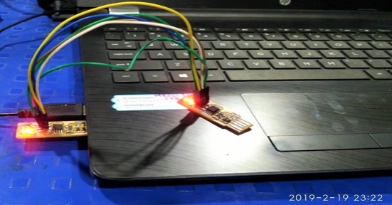
Then I connected them with jumper wires and started programming on my laptop.
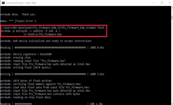
I ran the following commands.
make flash
Using this command I burned the program in my board using another FabISP.
make fuses
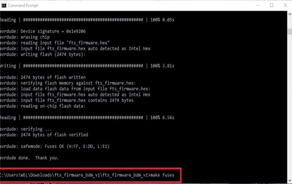
Fuse memory is a separate chunk of flash that is not written when you update the firmware.
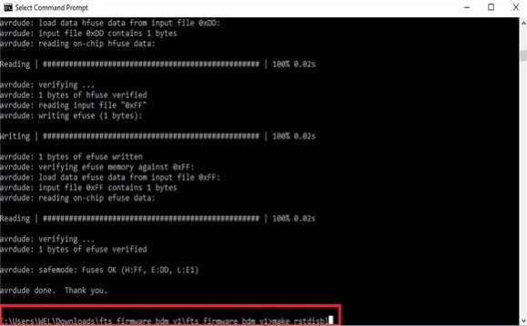
make rstd
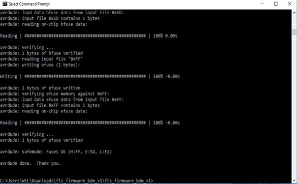
Using this command I made my board as a Fab ISP Programmer.
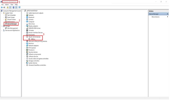
Testing the Fab ISP Programmer – After completing the burning process, I checked my Fab ISP Programmer by connecting my Laptop using the Male-Female USB cable. Then I checked in Computer management>Device manager>libusb-win32 devices as shown below.
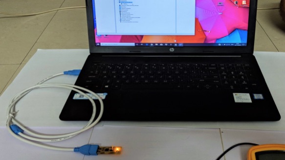
My USBtiny device is now showing in the 'Computer management>Device manager'.
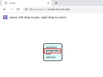
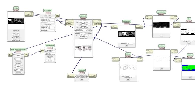
 Exploring Mods in browser recommended by firefox/chrome.

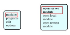
Then Right click anywhere and select PROGRAMS -- select OPEN SERVER
PROGRAM

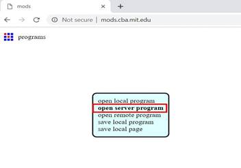
Select ROLAND > MILL > SMR20 (choose the machine you will
use)
I added another module to save the file automatically. So looked for the program/component that outputs the file. Then, I Right clicked anywhere in the white space and selected MODULE > OPEN SERVER MODULE > SAVE FILE. Then connected the elements by clicking on OUTPUT of RolandSrm-20milling machine and clicking again in INPUT of save file module to make the connection/ wiring between them.
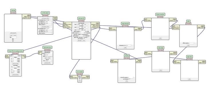
Opened my traces of the image file - Go to READ PNG MODULE SELECT- PNG FILE - selected traces image.
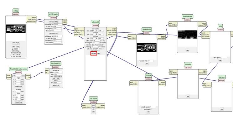
SET PCB Default module and click in MILL TRACES.
 <
<
For saving file. Right click-->Modules-->open server module.
file-->save
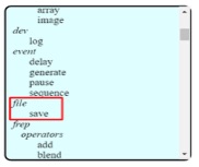
Then I joined the Input file to Output file.
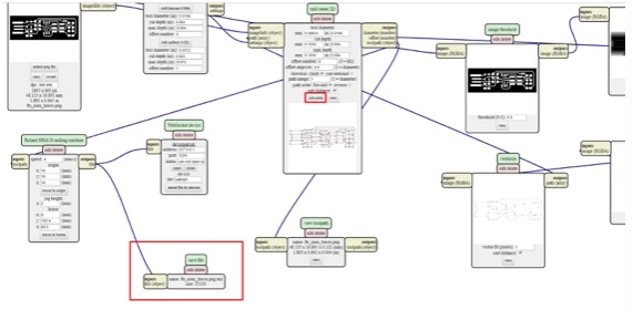
Mill Raster 2D Module click in calculate. When done, the file was
saved automatically in my download folder. I have also made a flexible
PCB.
Flexible Fab ISP - I have also made a flexible PCB on the Vinyl Cutter.
Procedure followed -
I’ve downloaded the .png file from Brian and opened it in the terminal.
Commands used -
Sudo Fab
Enter password
From input format select (image).png
Selected Roland Vinylcutter (.camm)
make_png_camm
Then I loaded .png file and sent it to the Vinyl Cutter.
I’ve cut the print on Vinyl Sheet and removed all the unwanted parts by using the X-Acto knife. As seen below, it’s ready and working.
This is the png file trace - A5 Electronics
Production_files\fts_mini_traces.png
This is png file cut - A5 Electronics
Production_files\fts_mini_cut.png
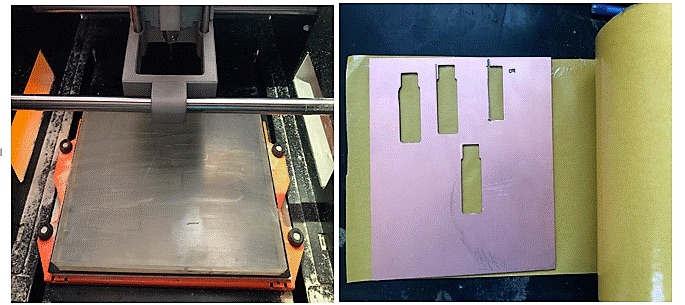
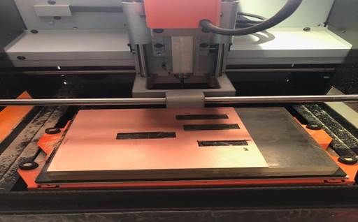
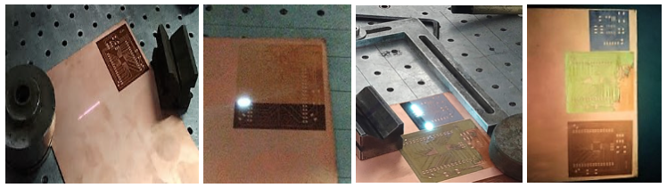
Research, Trail & Error I have tried out my pcb
design on this laser metal engraving machine from a commercial vendor
Fine Mark Laser Engravers in Hyderabad after going through the
following link as shown below.
http://fabacademy.org/archives/2015/doc/fiber-laser-cutting-pcb.html
This is the first trial – Power 95, Frequency 10,000 and Speed 300 on
10 watts on 5 passes.
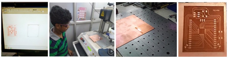
The second trial – PCB was burnt after 3 passes.
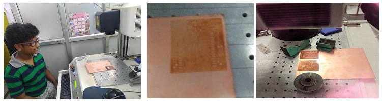
The third trail – On another machine with Power 80, Frequency 75,000,
Speed 600 on 50 watts on 12 passes.
You can view the videos from this link below –
https://photos.app.goo.gl/1mcs6J8xZUdErJMQ8
Design file –
A5 Electronics
Production_files\new
uno.brd
Learning Outcome – I have got an idea about PCB
milling and programming by doing a lot of learning and relearning,
while unlearning. Must admit that my soldering skills have improved
now. The fab modules on browser using MODS to ease the process was
exciting. Now I glad that I have made PCBs, make a Programmer and
Program it on my own.
Reference –
http://fab.cba.mit.edu/classes/863.16/doc/projects/ftsmin/index.html
http://fabacademy.org/2019/docs/FabAcademy-Tutorials/week04_electronic_production/srm20_windows.html
http://fab.cba.mit.edu/classes/863.16/doc/projects/ftsmin/windows_avr.html
https://www.microchip.com/mplab/avr-support/avr-and-arm-toolchains-c-compilers
http://fabmodules.org/mods.html
http://fabmodules.org/mods.html