Electronics design
This week on the menu, electronics design. This week follows up on week 5, electronics production. It was a fun week that I was really look forward to. Week 5 was my first real experience milling PCBs and soldering PCB components. I liked it and since everything worked quite well inmediatly I felt confident about this week. Boy was I wrong. A lot of things went wrong and most of them were quite silly. For example my wonderfull Macbook (running Mojave) disliked KiCad, or KiCad disliked my Macbook. This gave super weird crashes that only periodically and unpredictable happend. I installed the newest builds, older builds, nightly builds, and it just kept happening. After a few hours of trying I threw in the towel and moved on to a old Windows Surface tablet, that worked inmediatly. The next main issue I had in retrospect was the ISP, I remember it working two weeks ago. I had followed all the steps in the process to the letter and it worked. I put it in my bag and only tried it again this week. Surprise, it didn't work anymore. It was only rarely being recognized by my Mac, with or without USB 2 hub, with or without a cable, left or right USB internal port. Since I thought it was the Echo board being at fault I was just groping around in the dark. Back at the Waag my instructor, Henk, also had difficulty connecting to the ISP - it didn't work at all at this point. He told me to debug the ISP and take it from there. Once this was fixed I was hopefull the Hello Echo board would just magically work. Guess what, it didn't.
My knowledge on electronical components is limited. I followed physics classes in high school and played around with Arduino's in the past. I knew about polarity being a thing and recognized most part names. So this week I learned a lot about what these componenets actaully do, how to connect & check them.
Electronics design
Hardware
USB drive
Modela MDX20
Soldering iron - Weller WS 81 (SMD tip)
Artisjet UV printer
Software
FabModules
KiCad
Photoshop
Tools
1/32 inch milling bit
1/64 inch milling bit
Scraper
Materials
FR-1 PCB blanks (1.8 mm thickness)
Double sided tape (good quality)
Rubbing alcohol
Electronics
We started this week with some basics electronics. What do the parts and how can we see their functionallity on a board. For the group assignment We looked at a multimeter, regulated power supply & oscilloscope.
Formfactor and size
There are a lot of different parts in the electronics world - parts with the same functionallity come in different forms and sizes. The first one is Through-Hole Mounting (THM), these parts have big leads sticking out, these are the ones I've seen most. The the other one is Surface Mount Technology (SMT), these are the parts that were used on the ISP board in week 5. The SMT parts are a lot smaller and don't need any holes to mount them to a PCB. This ease of use and the size are the reasons we use them in the Fablab. The SMD parts can also have different form factors, we will use the 1206 (imperial) or 3216 (metric).
Power, current, resistance and watts
All of these parts combined can make really cool stuff - like arduino's or sensor kits. All parts have different functionallity and need different specifications - this makes it a bit challenging to make things. For example, you can have two parts in your system that need a different amount of power - you need another part to lower the power for one of the parts.
Everything around us that works on electricity needs power to work. There are different kinds of giving this power (AC or DC) for example from batteries or from wall sockets. The current in these examples are different, from the wall socket we get alternating current (AC) and from the battery we get direct current (DC). The current indicates the direction whilst power is the actual pressure. It's really important to know about this since some parts break when they get an unexpected current.
Power is indicated and measured in Volts (U or V), it indicates the electric pressure. We will be using DC for our projects - powering a projects with this method requires a power source with a postive (+, VCC, anode) and a negative lead (-, GND, cathode). We imagine the power moving from the positive lead to the negative source. Using a regulated power supply, battery or USB connection we can power projects - we don't need a lot of power.
The next thing we need to know about is amps (A), the current. Just like volts, a minimum amount of current is needed for parts to work and these can differ between parts. To change current resistors (rated and measured in ohms, O, Ω) are used, they work like squeezers on a power line. With these basic units, volts, amps and ohms, it is possible to calculate what we need using Ohms law. All three units are relateda and we need to know at least two out of three to complete the calculation.
Ohms law
V = R * I
I = V / R
R = V / I
To make the circle complete we also need to know about Watts (W or P). This is the electrical power calculated by multiplying volts and amps. Also on specification sheets of parts you will see this value.
W = U * A
Parts
In a schematic drawing of electronic designs we can see the parts that are used. There are a lot of different parts but for this week we will focus on some of the most common ones. In schematics letters are used to indicate the kind of the part (and value).
| part | schematic |
|---|---|
| resistor | R |
| capacitor | C |
| inductor | L |
| switches | S |
| transistors | Q |
| integrated circuits | U |
| crystals and oscillators | Y |
| diodes | D |
Resistors
Resistors reduce electrical current by a precise amount. In a circuit you typically have a fixed input voltage, and resistors offer a fixed amount of resistance. Ohm's Law can be used to determine how much a resistor will limit current.
Orientation: no polarity
Testing: multimeter set at volts V

Capacitors
A capacitor is a component that stores electricity and discharges it back into the circuit when there is a drop in voltage. Capacitors are measured in Farads, which simply is symbolized with a capital F. Orientation: some capacitors have polarity. Testing: multimeter set at capacitance –|(–

Inductors
A inductor is a component that steadies current in a circuit. Inductors are measured in uH (microhenry).
Orientation: some inductors have polarity
Testing: multimeter set at Ohms - should be very low resistance

Switches
Transistors
A transistor is an electronic component that takes a small amount of current and amplifies it. A common transistor has three pins which are the base, collector, and emitter.
Orientation: polarity
Testing: multimeter set at Ohms - meter should deflect for both collector and emitter.
Integrated circuits
An integrated circuit is an electronic circuit compressed onto a small piece of silicon. Orientation: Indicated with a dot at the first pin Testing: difficult - check orientation and for shorts.

Crystals and oscillators
Crystals and oscillators are electronic components that produce oscillating electronic signals. They are important for the timing of the IC. They are both measured in Mhz.
Orientation: no polarity
Testing: Using a oscillator

Diodes
A diode is an electronic component that allows electricity to flow through in one direction, and all but stops it from flowing the opposite way. The diode's primary role is to route electricity. This is extremely useful for preventing an electrical signal from taking unwanted or unexpected routes within the circuit. Orientation: polarity Testing: multimeter set at continuety mode

KiCad
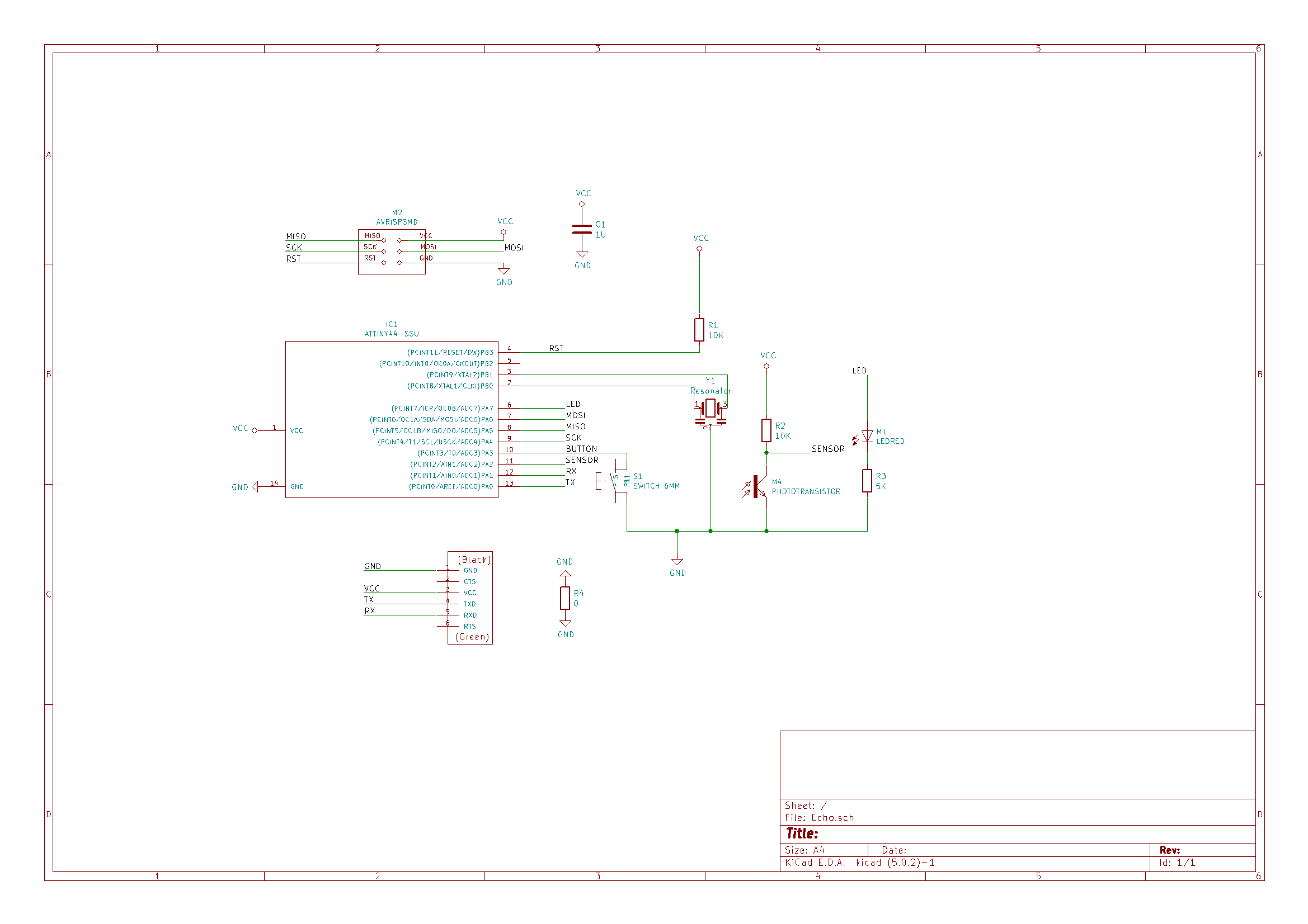
Kicad is a open source electronics design suite - it makes schematic drawings and helps you translate them into a file that's ready for milling or for outsourcing. It was my first time using this software and it looked overwelming at first but quickly it got easier. KiCad should work on all platforms but I found that Mojave wasn't compatible in praxis - it kept crashing. Even after installing special dependancies from the builder and different versions it was still failing. As far as I could find it should work up to Mojave 10.14 (I run 10.14.3). Someone in the group with the same OSX installed was facing similar issues so we ended the day with using different computers - a old mac and a old windows machine. Both worked perfectly. Another back up plan was to install a sandbox enviroment running an older OSX on my current machine and try to install Kicad there. This would take up quite some time so I was happy not to go down that route. On Windows 10 it worked inmediatly after installing.
The software is quite interesting, it is basically mutliple programs combined. Each program has their own task and they need to be used in order. You start in the schematic capture enviroment by collecting all the parts, than you place them in a schematic and connect them. This is the most crucial part - any mistake in the schematic will lead to a mistake in the PCB. For example, I used buses instead of wires to connect parts - these don't show up in the PCB lay out area. The same goes for open gates or missing links - they don't magically appear. To go to the next step you need combine the components to their respective footprints - this is all done in the same enviroment. From this you can export it and open it in the PCB lay out area - the schematic gets translated into a bunch of footprints that are linked and from here the puzzeling begins.
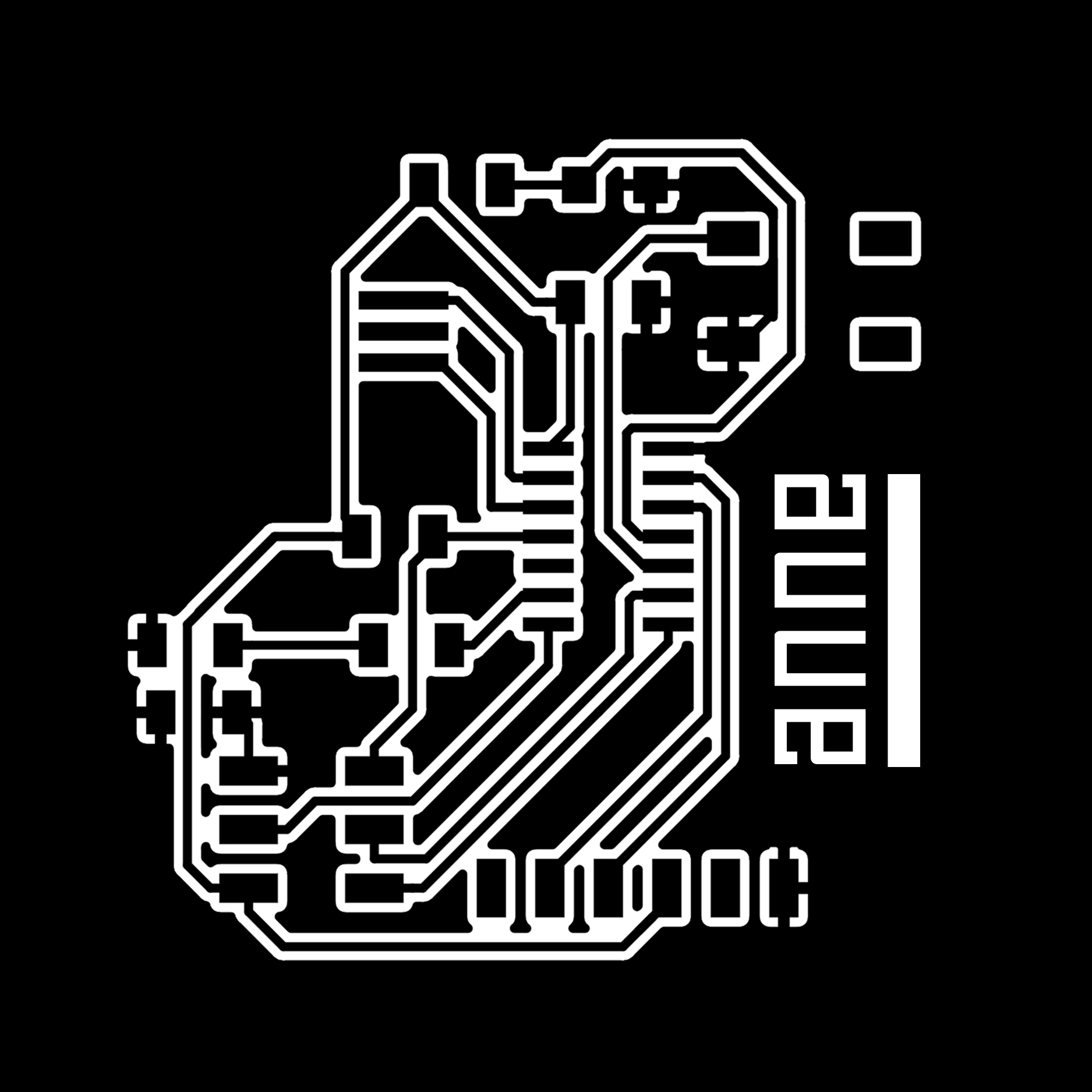
Once the footprints and their links arrived in this area its a big mess, a rats nest. The white wires indicate what parts should be connected - although it being a bit random, part with a GND will only show one option for a connection while in reality you can link it to any other ground, as long as they are all interlinked in the end. Parts are also on top of each other and not necessarly in the right orientation. By moving them around and linking them together with tracks you can create some order. The goal is to arrange things in a way that is space efficient, everything connected and somewhat logical. For example, if you need a FTDI connector, place it to the side and don't hide components where you need acces to connect. Parts that belong together should kind of be in the same place. Also it's best practice to orientate parts that are the same form in the same direction, this makes for easier soldering. I would also to advise to use a bit more space inbetween parts to make things less messy, this is easier for debugging later on since you can see what parts should be connected.
The adding of tracks was the most time consuming part for me - I tried different techniques. The first one, moving all parts around and just trying. This failed. I was having to change tracks and move parts constantly. Than I started with the IC and added components one by one going from the components with the most connections (for example the header pins) towards the simpler connections. This was also not really working for me. Than I asked Google, no real luck there. Basically you need some experience to do this well. In the end my technique improved to something that worked quite well. Start the IC and route as many tracks as you can underneath, next the other big parts and do the same thing. Now keep adding left over components like resistors and use them to cross tracks that are already in place. From here on out you can export your file fore milling and everything should be fairly straightforward.
Step by step guide
- Download and install KiCad - make sure to also download and install the fab specific libraries. This is done via the menu Prefrences > Manage symbol libraries in the schematic capture enviroment. And in the Assign footprint menu > Prefrences > Manage footprint libraries.
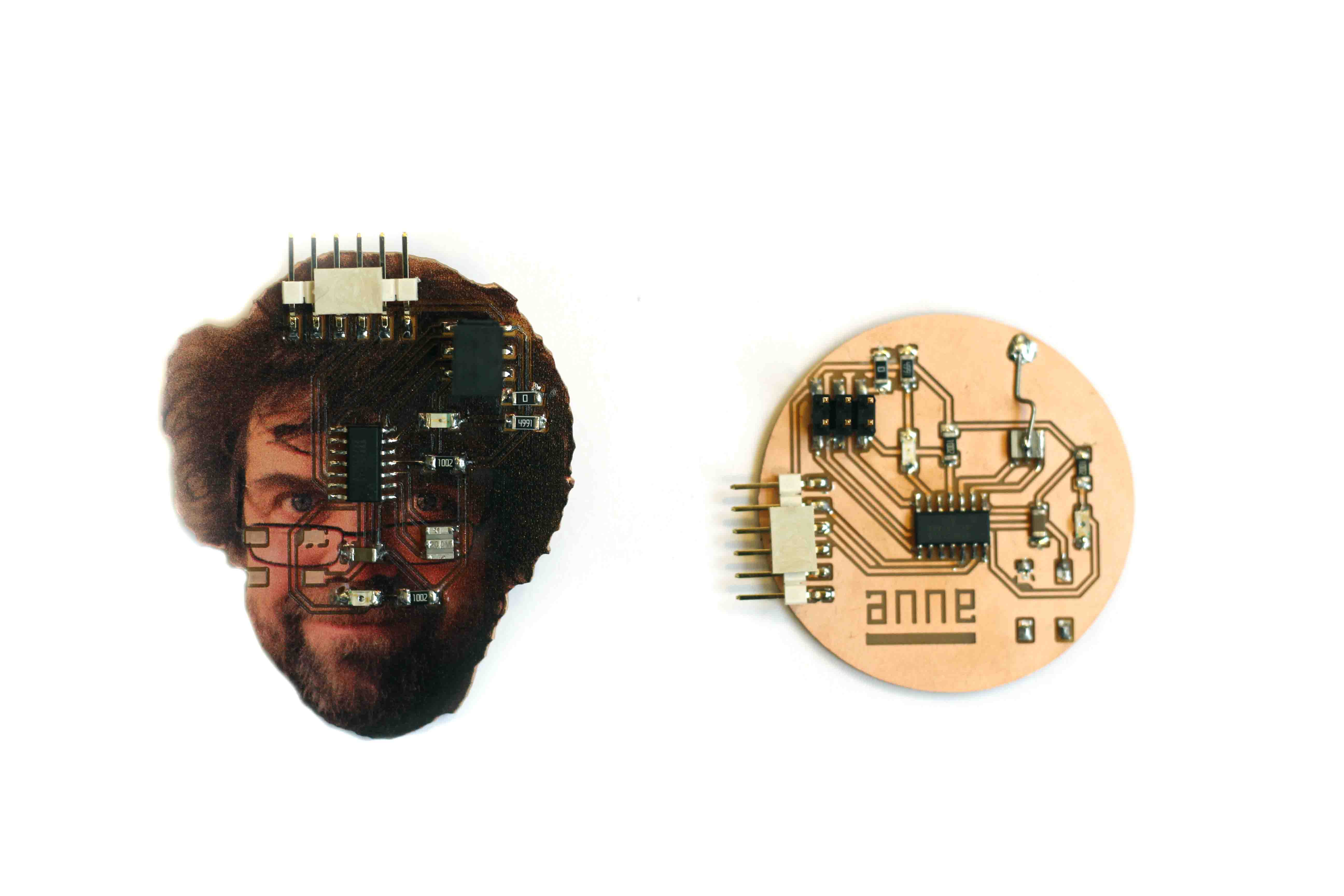
- Start with what you want to make - for me it was making the Hello Echo board. I received an excisting schematic as a .png.
- Start a new project File > New > Project and give it a descriptive name.
- Open the Schematic Layout Editor.
From left to right in the menu you see, the schematic layout editor, symbol library editor, pcb layout editor, footprint libary editor, gerber viewer, import bitmap, calculator and worksheet layout editor.

- By using hotkey A open the Choose symbol screen. This shows you the nearly 13 thousand components that you can pick from. By typing 'fab' you can go to the special Fab components. Pick your symbol and press okay or hit enter. The symbol can now be placed anywhere by clicking. Add all needed components.

- Rotate (R) or move (M) your symbols to where they make sense, this can always be changed. This is all about making a good schematic and not yet about the production. Spend some time making a clear schematic.
- Make all connections between parts that should be connected, this can be done in two ways. The easiest way is with a connected wire. Move your cursor over the link you want to connect and use hotkey for wire (W) drag it to the place you want to connect it to and close the wire (K). The second way of making connections is with two wires that get labled the same name. Make an open wire to you component and hover over the open end to make a label (L). Give the label a descriptive name. Also do this for the 'other half' of the wire. These should now automatically be connected in the PCB lay out editor.

- Add the correct values for each part by doubleclicking the icon (or pressing E) - a Edit Value Field window will appear where you can change the text to the correct value.
- Continue to the Annotate schematic symbols. Click annotate. This will automatically number all parts with unique names. A letter for the part kind and a unique number.

- Once your happy go to the Assign Footprint Editor. There are three colums, the middle one is our list. Select the first line and find the correct folder in the left column, select the correct footprint in the right column. Do this for all lines and press Apply, Save Schematic & Continue. This is also a moment to save our project again.

- Now it's time to leave the Schematic editor and continue to the PCB Lay out editor. To do this we need one last file where we save all connections, components, footprints, names, etc. This is a Netlist. Click Generate Netlist and save it in your project folder. Click Run PCB to layout.
- A new window should pop-up. Before anything else we change the design rules (Setup > Design Rules). These values work well for the Modela but if you use a different machine you should first test it's capabillities. Safe again to make sure you don't lose these settings.

- Import the ratsnest. Tools > Load Netlist, click to place it. FYI If you make any changes in the schematic and safe the netlist again you can simply use Update PCB from Schematic. This keeps all your current work and adds the changes.
- Move (M) and rotate (R) all parts to where you want them.
- Connect all parts with track (X) - make sure to connect everything.

- Draw a cutout shape around your board - if you want to make something more than a square or circle this cannot be done in this software.
- Export your design via File > Export > SVG. Choose what layers to export and safe your SVG.

- Now it's time to mill, open the SVG in mods and follow the steps described in week 5.
Additional steps for creative boards
- Open your SVG in Photoshop.
- Adjust the canvas size if needed.
- Draw on a new layer the shape of your cutout in black and white.
- For full color boards use the shape of your cutout to make your design on.
- Safe all layers (traces, outline, artwork) and you are ready to mill.
- After the milling and before the soldering open your design in Whiterip.

- Go to templates.
- Select a work area with a margin and a color workspace in the top bar. Place your image on the bed.

- Start the printer (on/off button) and press Ready and UV, this swtichtes on the UV lights during printing and starts the startup procedure. Put some tape on the bed where you expect your design to print.

- Move the bed as close as possible to the top using the up and down buttons.
- Start your print. Put some double sided tape on your pcb.

- When the print is finished add your PCB on top of the print on the tape. Align carefully. Lower the bed a bit to compensate for the thickness of the PCB. Print again. The ink should be dry inmediatly.

- You can solder like usual - don't forget to clean the PCB again to get rid of any debries from handeling. The solder doesn't stick to the ink. I found that the soldering of this board was quite easy.
Test your board
After the soldering it's time to test the board. Connect your ISP en Hello Echo board and plug it in your computer. Go into the terminal and type the following line:
avrdude -c usbtiny -p t44For me this where most my trouble started - I got an error.
avrdude: error: usbtiny_transmit: usb_control_msg(DeviceRequestTO): unknown error
avrdude: initialization failed, rc=-1
         Double check connections and try again, or use -F to override
         this check.


avrdude: error: usbtiny_transmit: usb_control_msg(DeviceRequestTO): unknown error

avrdude done.  Thank you.
Plugging it into a USB 2 hub resulted in another error.
avrdude: initialization failed, rc=-1
         Double check connections and try again, or use -F to override
         this check.


avrdude done.  Thank you.
I was expecting my ISP to work and therefore my assumption was that there was something wrong with the board. So I started the debugging. I don't believe there is a perfect order in wich this can be done since each project is different and no error the same.
- Start with a visual inspection, what do the solder joints look like? Are parts straight? Where are the messy parts?
- Get the multimeter and test for continuety and shorts.
- Check if all the right parts are used and if the parts have the correct orientation.
- Check measure the parts with a multimeter (where possible) to check if they work as expected.
- Reheat all joints to make sure there are no cold soldered connections.
- Triple check your schematic.
- Try a different ISP.
- Try a different computer, ports, ribbon cable, hubs, etc.
- Try again.
No rippeling issues. The one issue I found was that I forgot to ground my resonator to ground. I fixed this with a small airgapped wire soldered to the top of the part and ground. The board should be recognized without the resonator so I still was no closer to my answer.
Next my instructor, Henk, had another look. He found that the ISP was not working at all anymore. Also the hub I had been using was giving issues. So debugged the ISP using the same procedure, no errors. The only thing I could think of was that during the masking I had to clean it a couple times, maybe I had cleaned it a bit to rough and cause a hairline break in one of the tracks. Henk recommended me to replace the IC.
I replaced the IC and .... everything worked. I reprogramemd the ISP the same way as in week 5 and checked if the Hello Echo board was now working. Ofcourse it didn't and I retested it again. When Henk tested it he remembered some issues with the button from last year. So I took of the button and also this was no solution. So after both me and Henk checking everything and not finding anything we replaced the IC. And it worked perfectly fine after this.
It's quite unlikely to have two bad chips so I must have done something wrong or one chip wrecked the other. It's hard to tell but everything works now. Next I had some time left over so I also soldered the Hello Henk board. This one worked the first time around.
anne@Annes-MacBook-Pro-352:~$    avrdude -c usbtiny -p t44

avrdude: AVR device initialized and ready to accept instructions

Reading | ################################################## | 100% 0.01s

avrdude: Device signature = 0x1e9207

avrdude: safemode: Fuses OK (H:FF, E:DF, L:62)

avrdude done.  Thank you.

Files
Hello Echo schematic
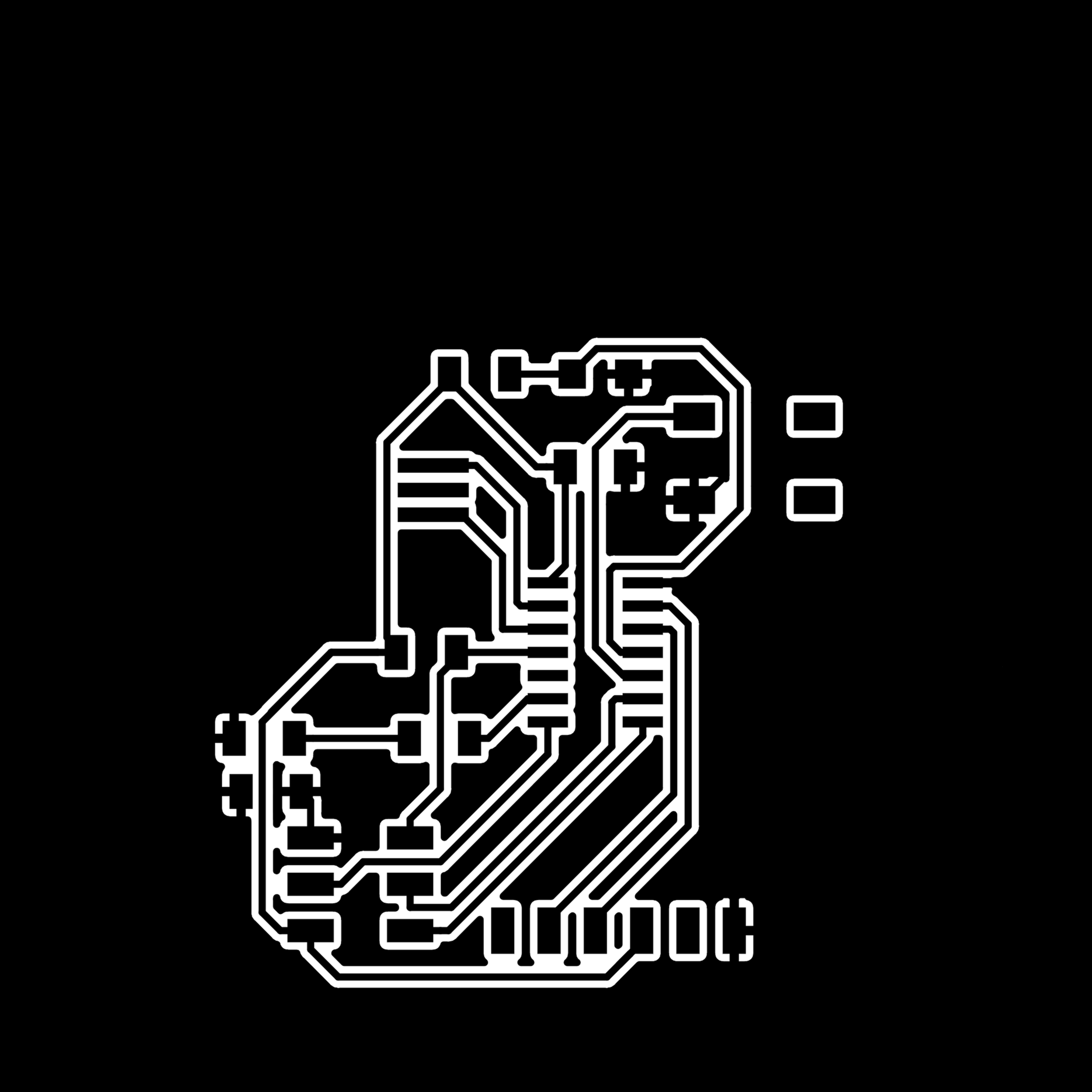
Hello Echo traces
Hello Echo cutout
Hello Henk traces
Hello Henk cutout
Hello Henk artwork
Hello Henk KiCad