Week 17: Invention, Intellectual Property, and Income
This was unfortunately my second week without my normal computer, but I was able to make the best of it. I finished the first round of CAD, printed the pill case enclosure, made appropriate changes to the model, re-printed the enclosure, and moved on to PCB design.
May 26
Neil’s lecture highlighted different systems for protecting intillectual property. Already disenchanted by the patent system, I was glad to hear that Neil discouraged seeking them. After the lecture, I reviewed the different types of creative commons licences. Regarding my project specifically, I would like to like to keep open the option to commericalize it, so I was interested in the Attribution-NonCommercial-NoDerivatives 4.0 International (CC BY-NC-ND 4.0) license. That being said, my journey as a maker has been made possible through open-source software and hardware, and I would love to contribute to the collective knowledge base, especially with something that I feel is as essential as the product I’m developing. I can see a scenario where I continue to refine the design and manufacturing of a “flagship” model that could be commercialized, but maintain an open-source “dev kit” that could be manufactured in a home fab lab.
For Traintrackr, I have researchered trademarks to some extent, but have become nervous that I would waste money and / or essentially shoot myself in the foot by improperly discribing, or mis-charecterizing the mark. Should I commercialize the pill case, I would like to trademark the name, logo, and slogan, but I would seek professional help to do so.
May 27
During our local node check-in, I asked for some help decoding the schematic of the Adafruit Huzzah32 ESP32 development board, so I integrate its power management components into my board. We went over the datasheet, power management page, and schematic of the board. We looked at datasheets of the components, and when I had a good idea of which components did what, and which I would need to incorporate into my board, I searched for them on DigiKey. They were in stock, and I added them to my cart, but by the time I went to chack out later in the class, all of the components were out of stock.
I needed to adapt or die at this point, so I decided to move the power management circuitry to a second spiral, and focus on getting the board up and running with ana external USB power bank connected to a mini USB port in the enclosure. I would also order a Huzzah32 board so if I had time, I could desolder the power management components and solder them on to a future version of the pill case circuit board.
May 28
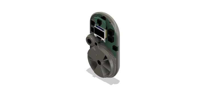
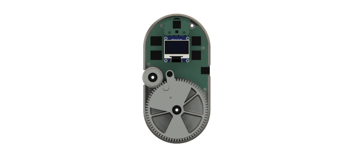
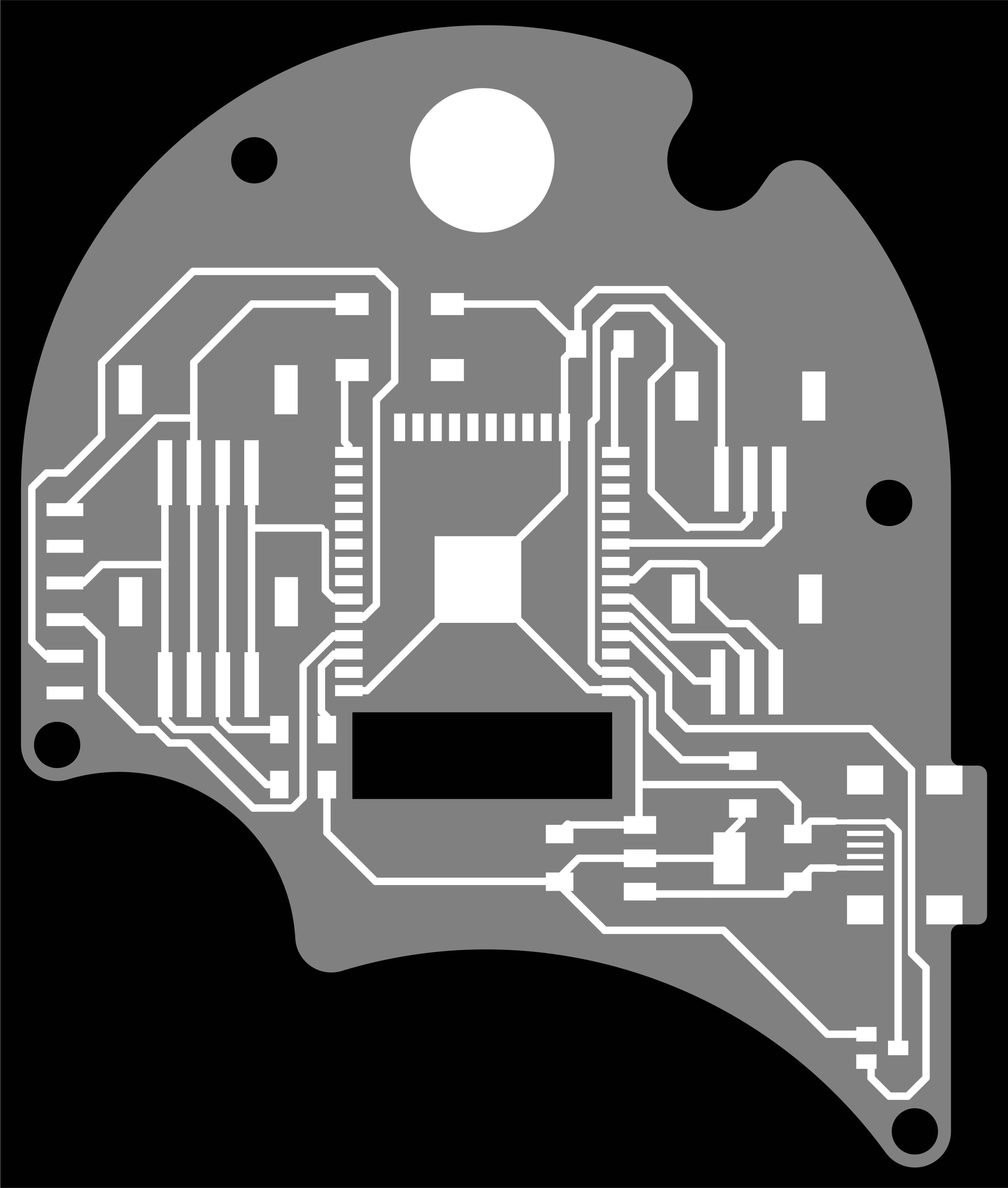
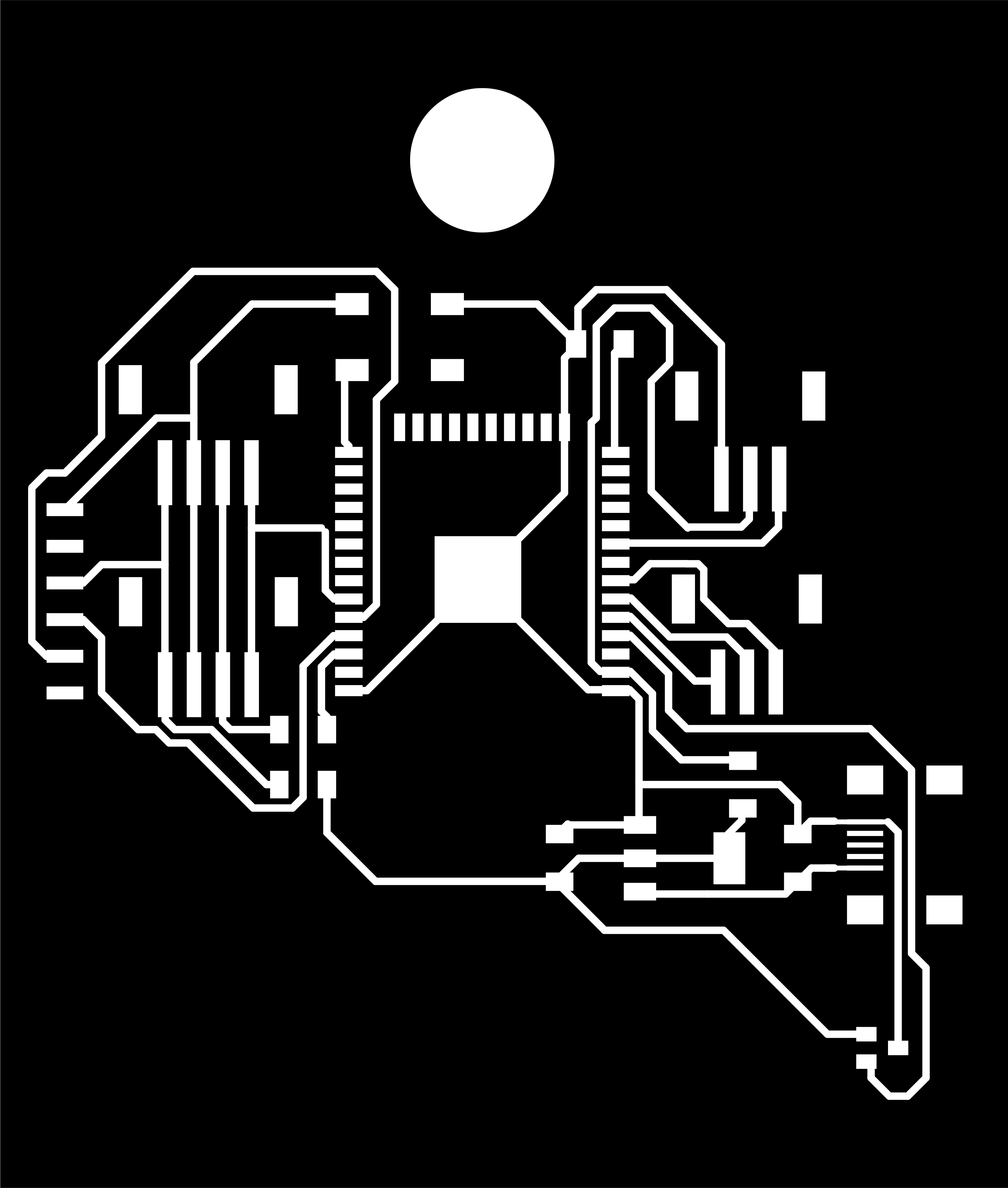
It was now game time. Two weeks until I would be presenting my final project. The clock was ticking. While the CAD looked relatively complete, there were still many small details missing in the enclosure, such as mounting holes, threadings, and clearances. More importantly, I had to model the screw heads and the connector terminals to make sure that components on the front and the back of the enclosure wouldn’t interfere with eachother. While there were components that had to be on the front face of the enclosure, my job was now to get as much as possible on to the main board. Not only did this cut down on the overall number of breakout boards I would need, but more importantly it would reduce the number of connectors, which are very bulky given the tight space. I moved the vibration motor and hall effect sensor to the main board, which went a long way. Unfortunately, I couldn’t mill the footprint of the MPU6050 accelerometer on the 1308, so I had to use the breakout board, but I was able to get clever and mount it behind the “feedback board” using the same mounting holes. Essentially, by overlapping in the XY plane where I had Z axis space to spare, I was able to free up some z-axis real estate where I needed it the most. This process was long, but necessary, and made it possible to move into the 2D world of PCB design without fear of creating a board with components that couldn’t fit in the enclosure.
May 30
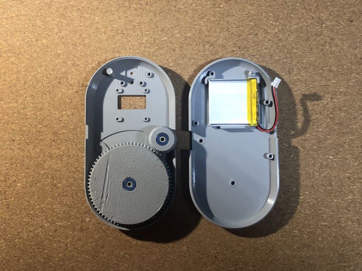
I printed out the enclosure on Printcess, and everything almost went perfectly. As you can see in the picture below, one of the threaded holes in the posts that connect the two halves on the enclosure was too short, and inserting the screw all the way caused the post to snap in half. This was a quick fix in CAD, and the second version of the part worked perfectly.
Enclosure Files:
May 31
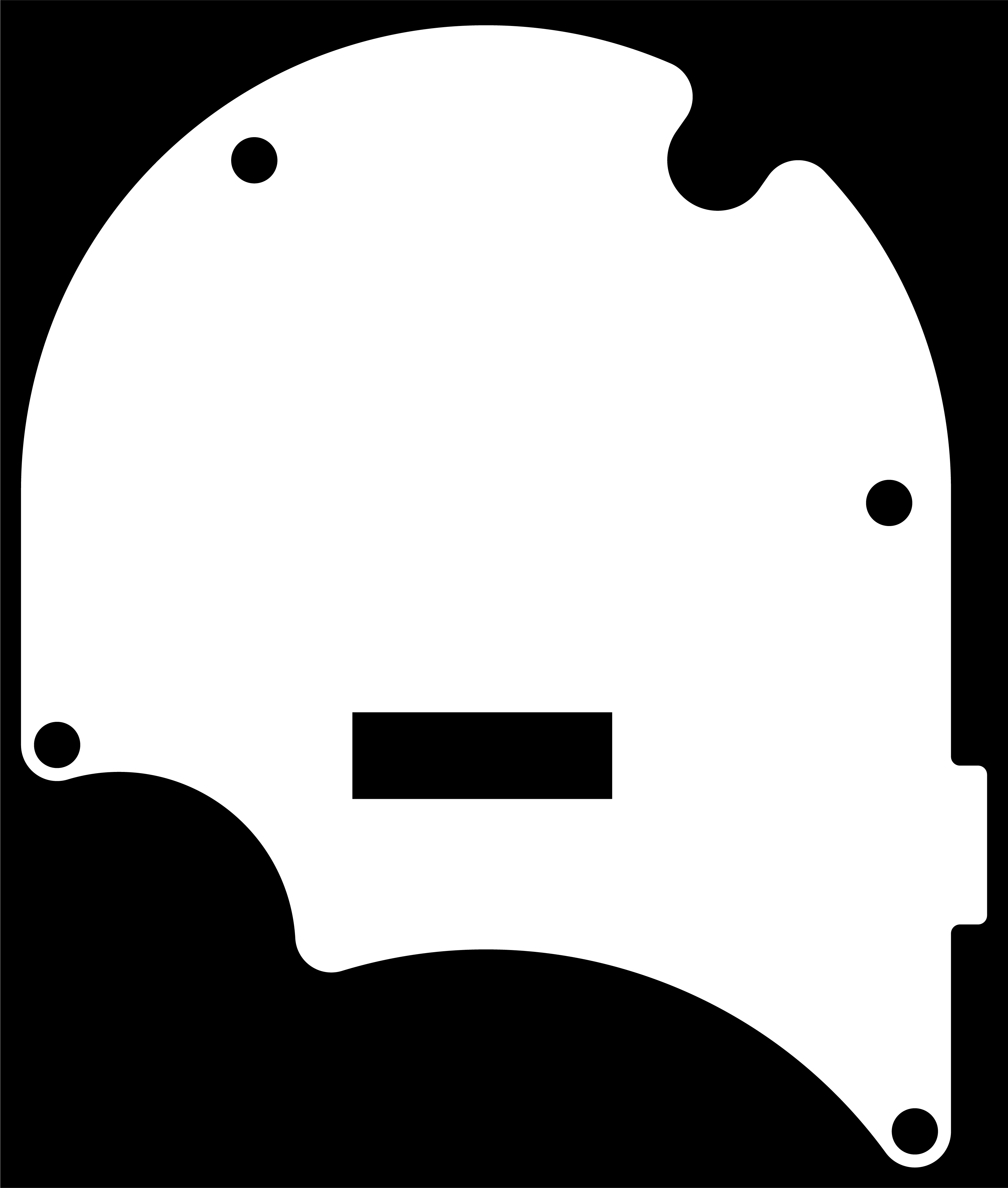
I exported a .dxf of the circuit board perimeter from Fusion, and attempted to load it into Eagle. interestingly, Eagle can only handle very rudimentary .dxf shapes for some reason, and no matter how I joined, unjoined, or chopped up the curvy shape, only bits and pieces of the board perimeter would load into Eagle. Fortunately, one of these permutations gave me enough of the shape to work with that I could accurately place all of the components, then I could just export the traces into Illustrator, where I could properly edit the perimeter vector file. Later on, I did find this tool to convert SVG files to Eagle scripts. In the future, I’ll give this a shot.
For the JST connectors linking the daughter boards to the mother board, I used JST-PH SMD connectors I purchased from Adafruit. I downloaded [this Eagle library] that contained THT and SMT footprints for vertical and horizontal connectors of a variety of sizes.
Jun 1
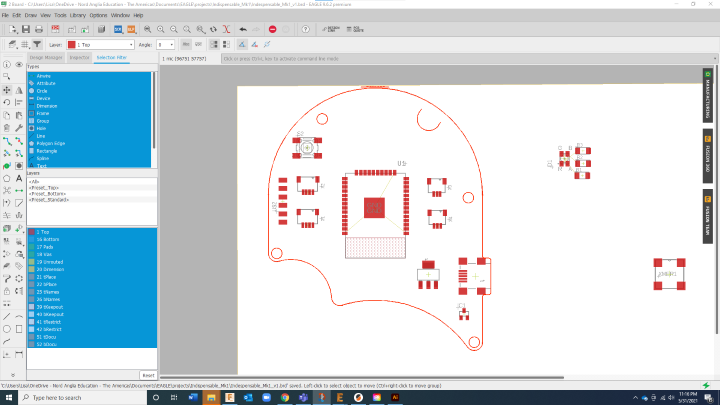
I created the schematic and board files, routed the airwires, exported the .dxf file into Illustrator, edited the files, and created the .png files that I will import into Mods.
I then generated a test slide and video file to serve as placeholders for my final project documentation.