Week4
Electronic production
Go to:Group assignment Individual assignment
Group assignment
Machine and tools
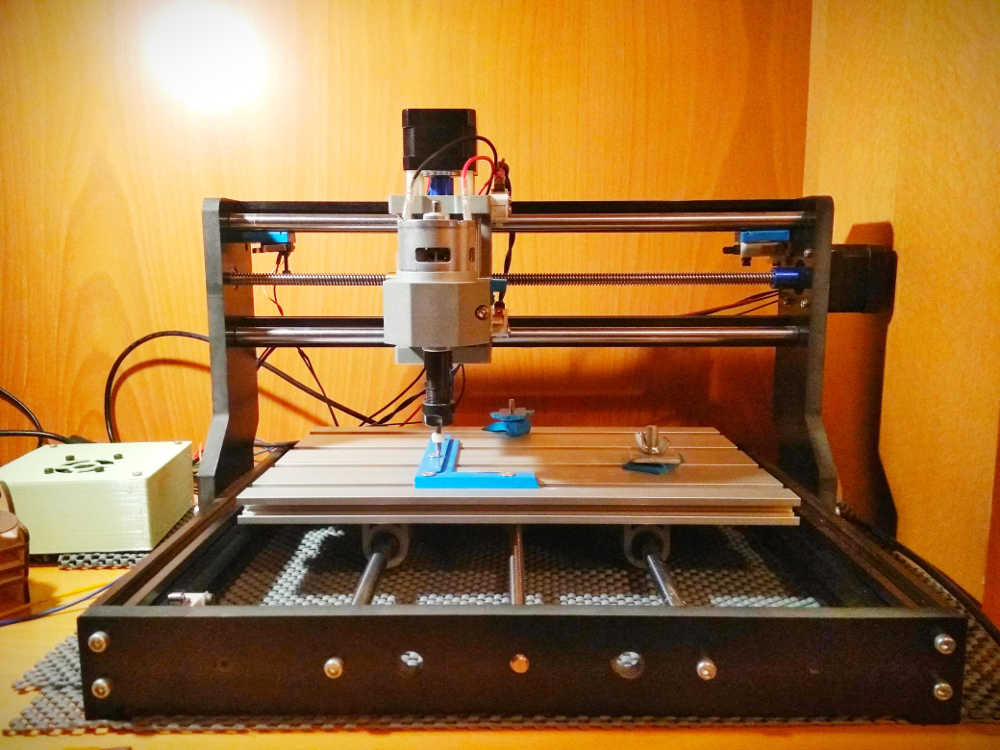
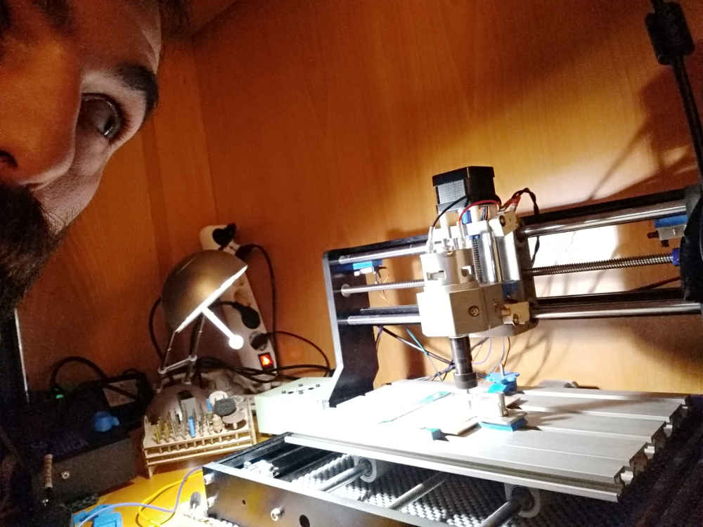
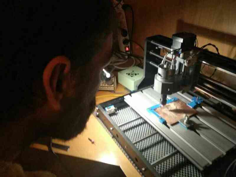
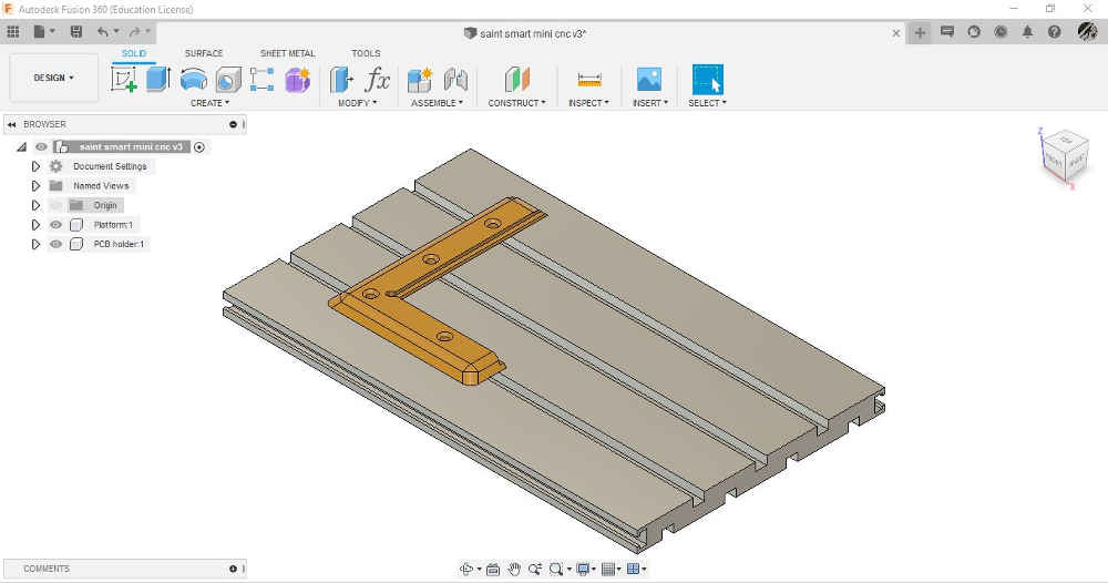
I am using a Saint-Smart arduino based 3018 small milling machine kit, I have made some modifications like adding end switches and removing the backlash on the axes and some that I have not had the chance to do yet...It's in a bit of a mess at the moment and apart from that, for now, it is working more or less as if it was out of the box.
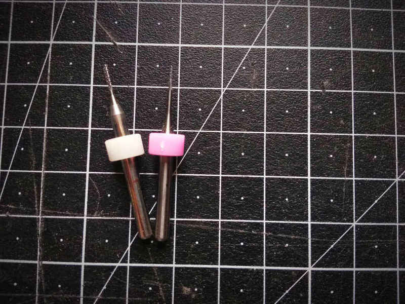
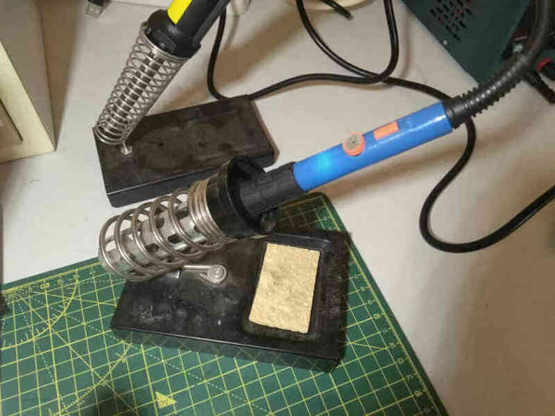
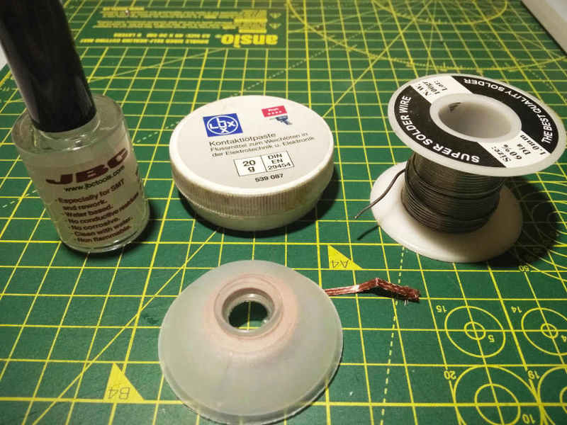
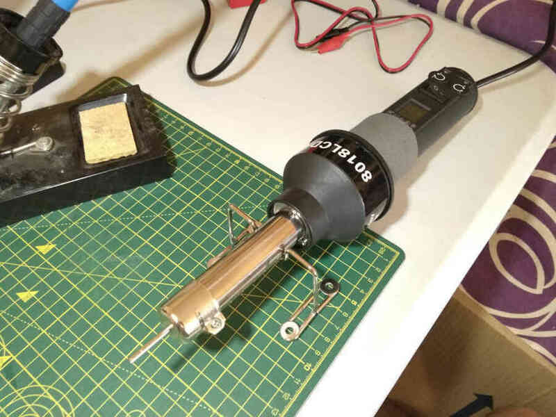
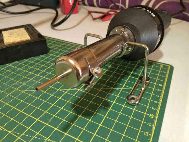
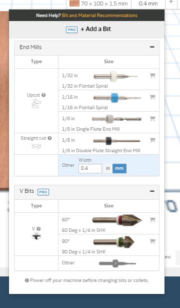
I will be using a 0.4mm flat end mill to trace and a 0.8mm flat end mill to cut the boards. A soldering Iron with a thin tip, flux, desoldering braid, solder wire and a heat gun with a thin exaust.
Characterize the design rules for your PCB production process:document feeds, speeds, plunge rate, depth of cut (traces and outline) and tooling.
To produce the g-code, I got the png file for the fabisp from this useful documentation
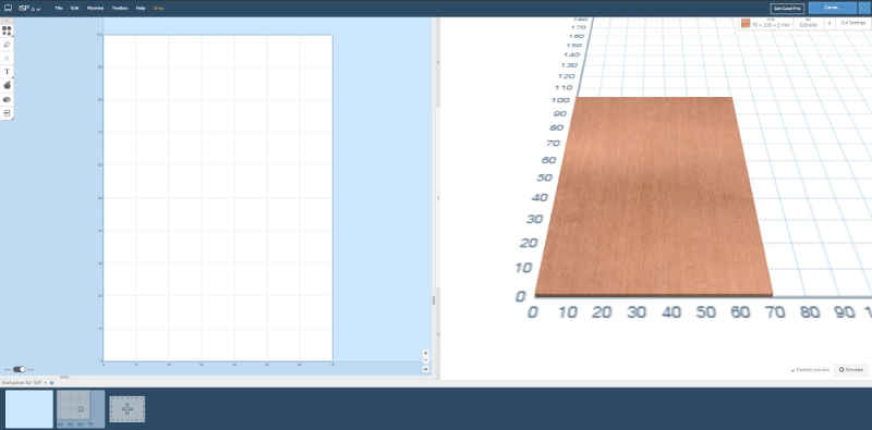
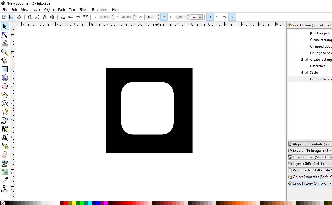
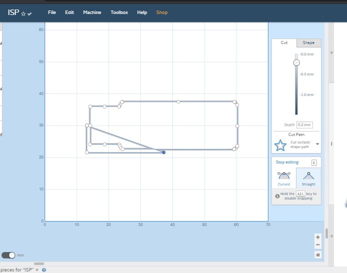
As I am using Easel (online cnc controller/design) to create the g-code for now, I am going to convert it into svg with inkscape to get a vector file (.svg trace and cut).
Easel (free account) is fairly simple to use, it does not offer a full range of parameters for milling found in other softwares and I hope to be able to design and prep the g-code in fusion for the final project, it also does not work with png files but it gets the job done…
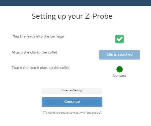
In Easel I need to set up the machine I am using, in my case, the Saint-Smart, I will quickly go through the machine set up:
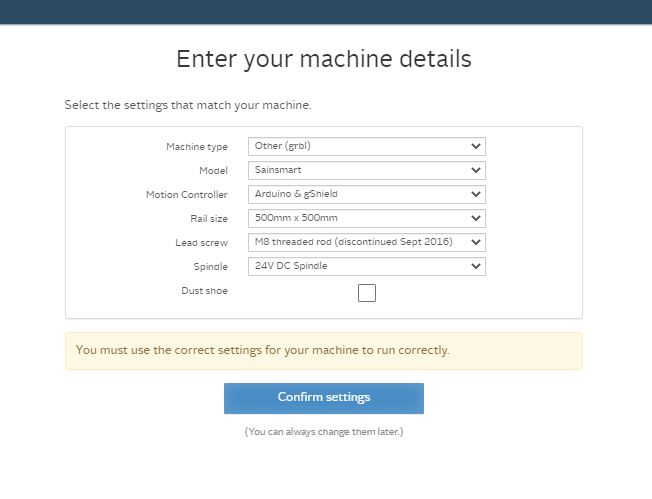
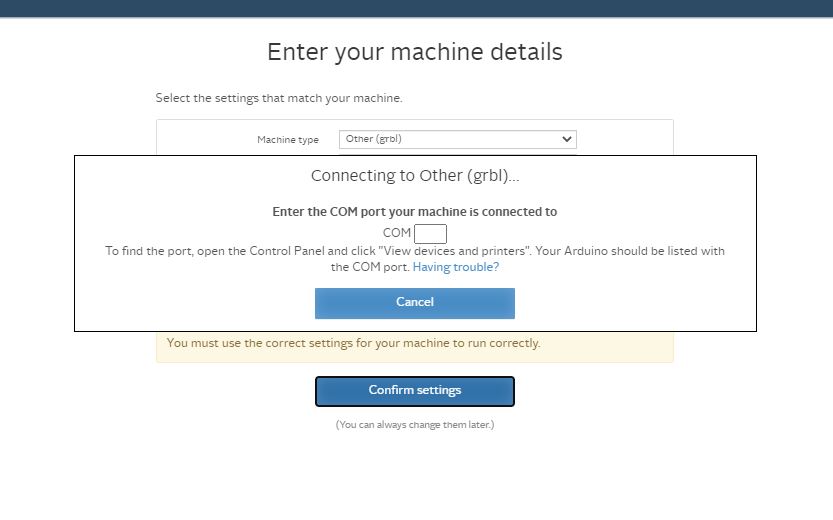
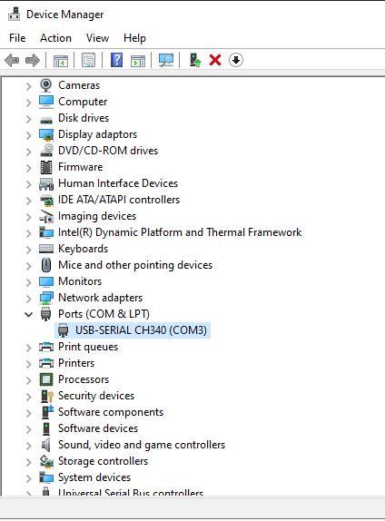
In “set up your machine”, specify machine type, model, motion controller, rail size, Lead screw type and spindle. Confirm the com port by checking the “Device manager”
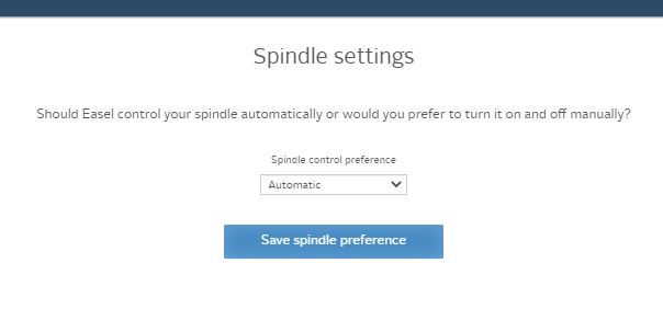
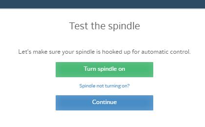
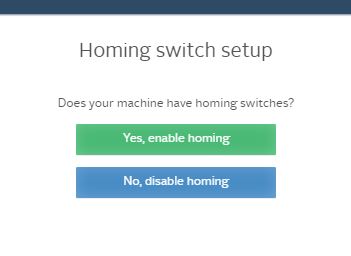
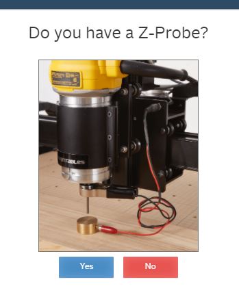
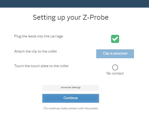
Then I have to go through a serie of check ups:
- Check the wiring

- Spindle setting and test it
- Homing switches yes or no
- Probe yes or no and set it up
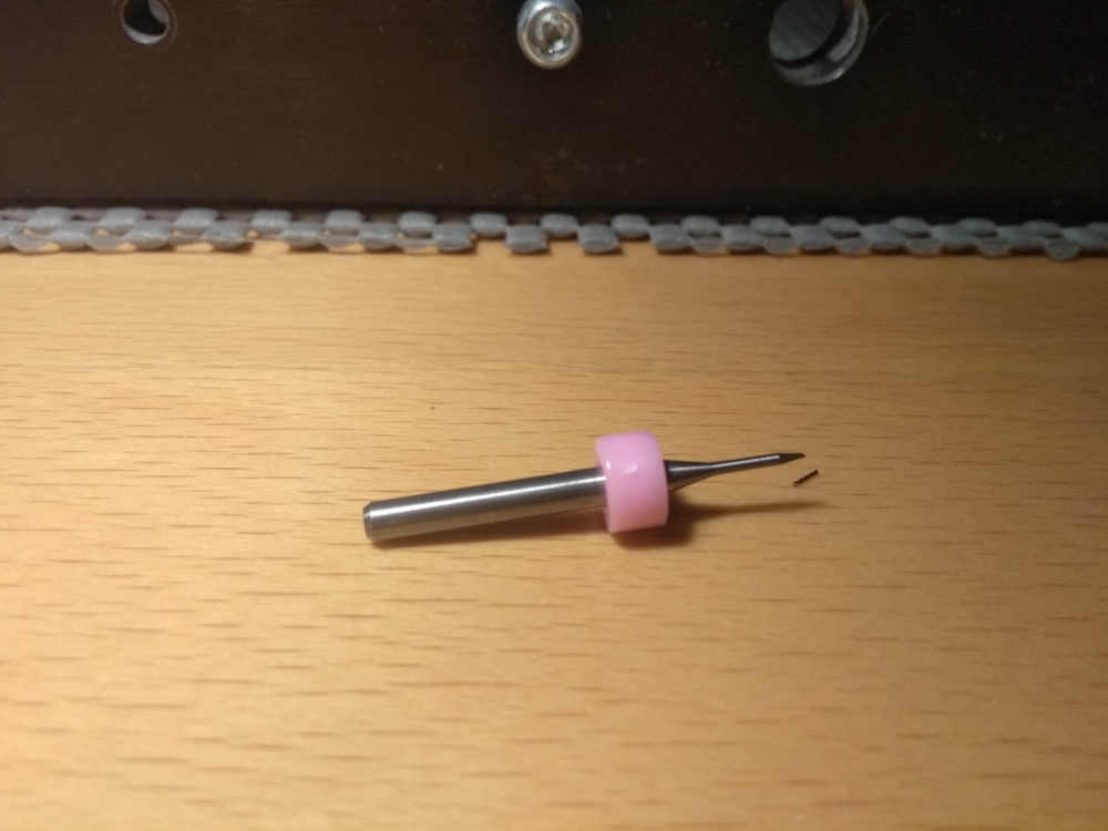
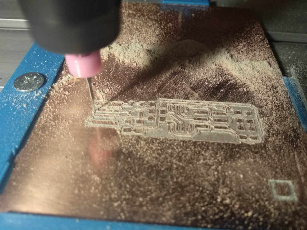
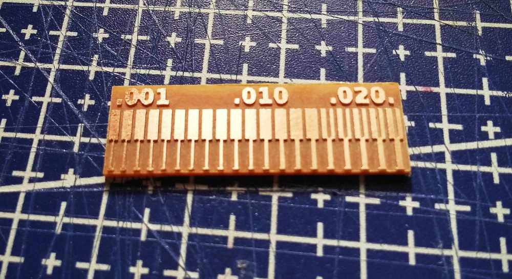
I made a quick and small test file to check my parameters with these 0.4mm bits, I don t think I ever used one that long before let's see how many I can break.
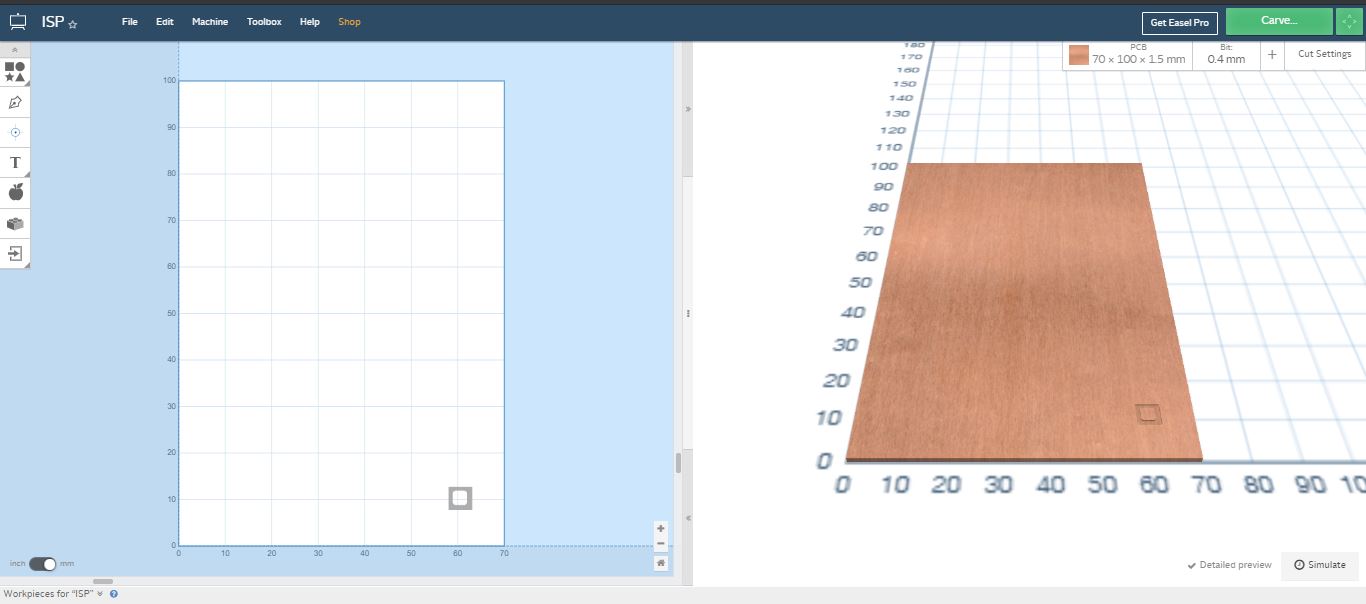
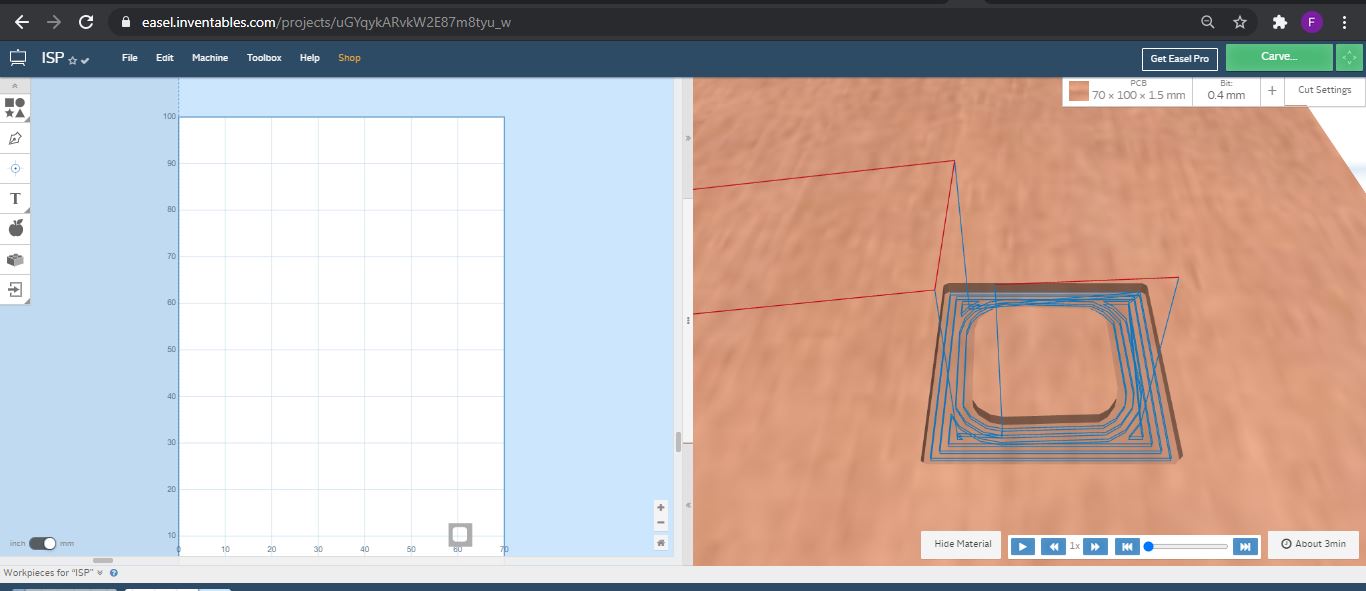
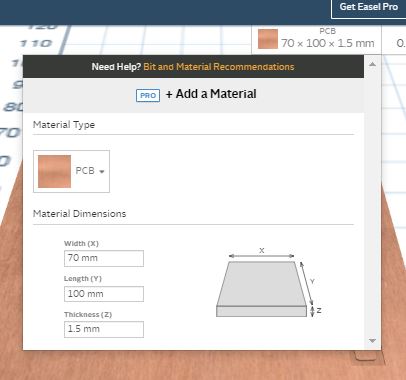
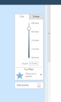
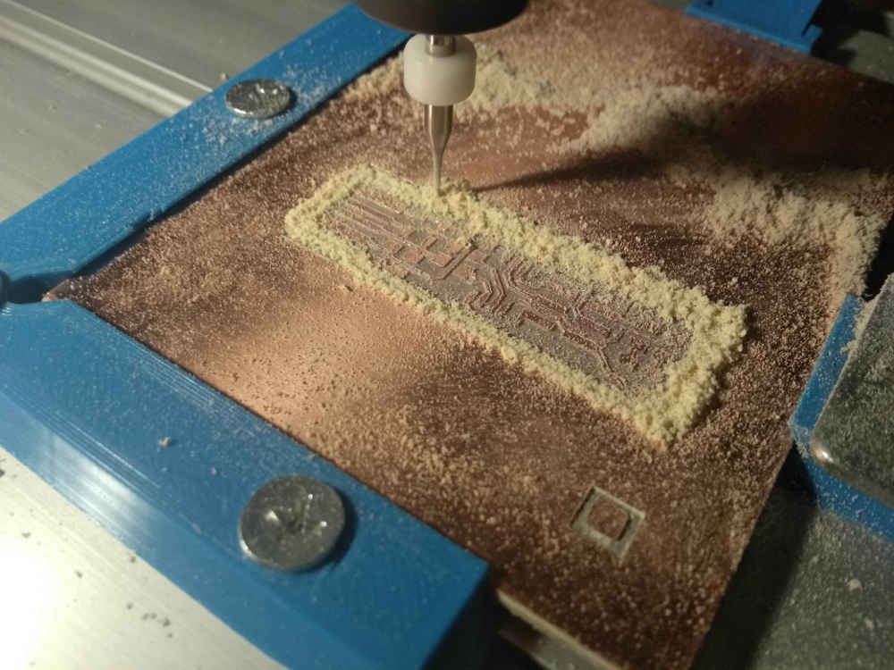
For the material dimensions, I am using a board of 70mm x 100mm, I measured 1.5mm thickness on this one
Then what bit I used, 0.4mm for the tracing and 0.8mm to cut it.
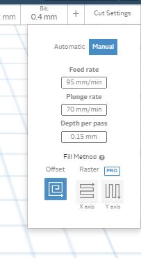
The feed rate, plunge rate and the depth per path. In my case I use a 95mm/min feed rate, 70mm/min plunge rate and a depth path of 0.15mm. Full depth of 0.3mm
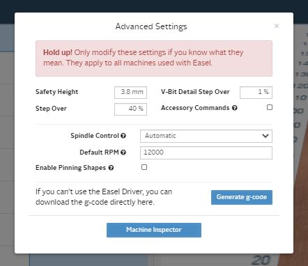
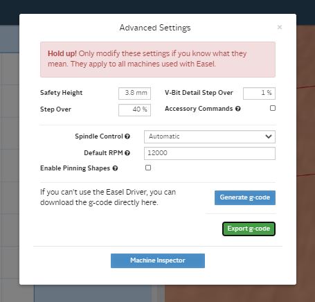
To get the g-code, in “machine” - “advance” - “create g-code” and “export”.
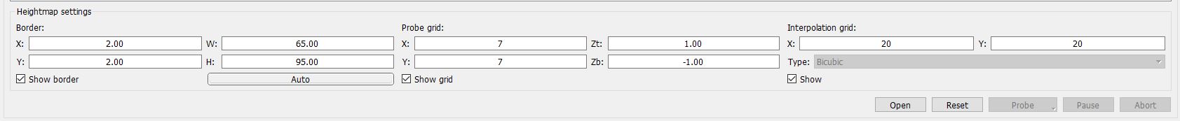
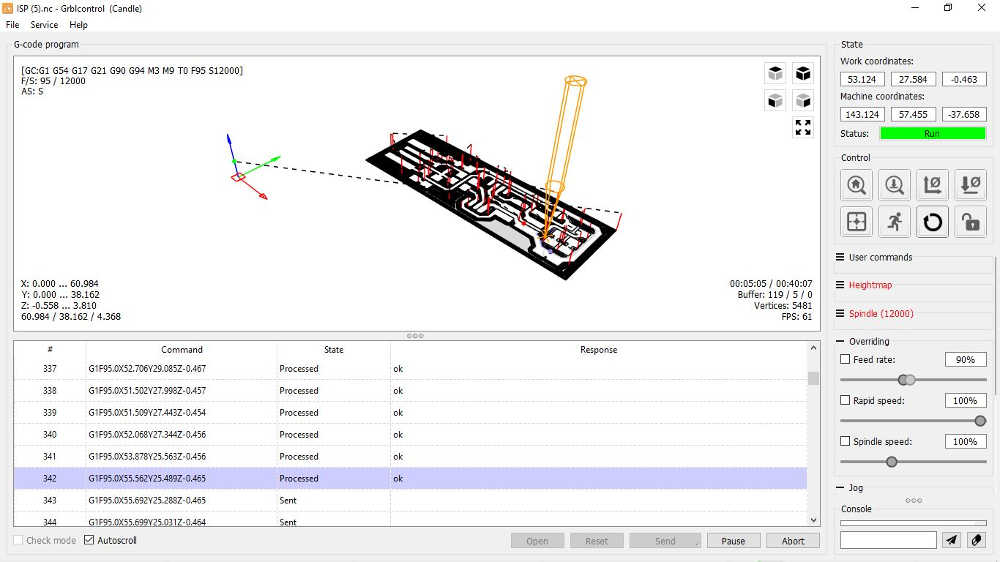
Once I got the g.code, I opened it in “Candle” (grbl control software) to produce a height map that helps with any un-leveled areas. With the g.code open, access the height map set up.
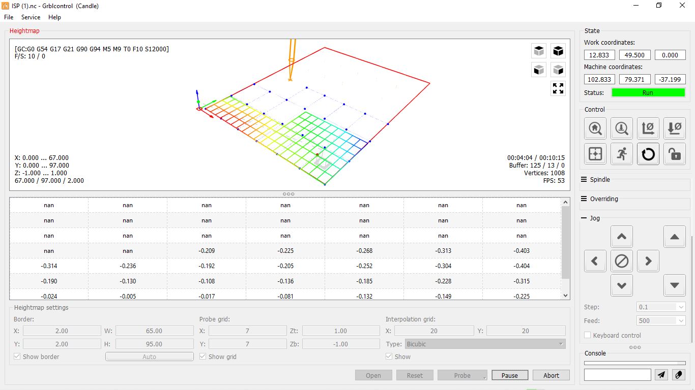
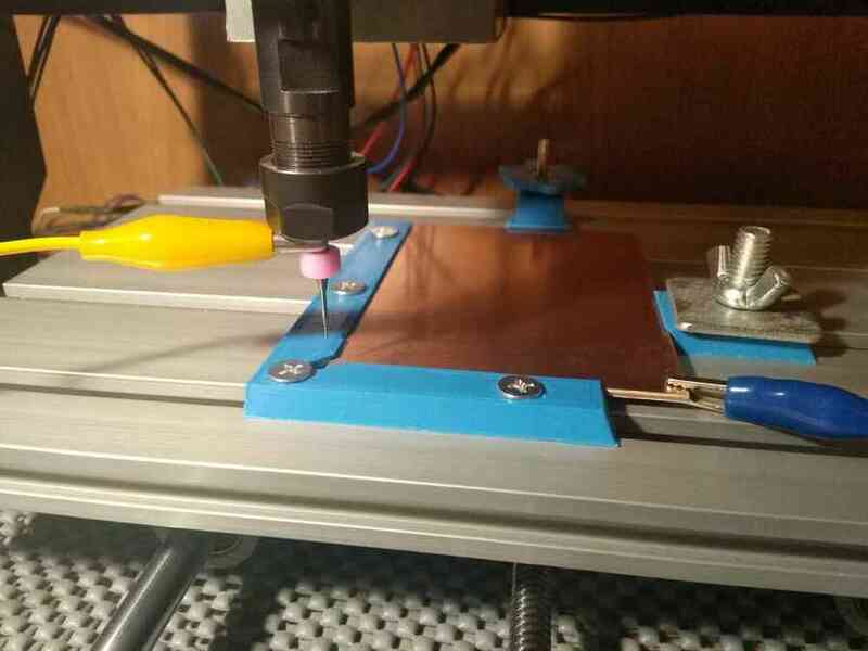
I set my material in the machine using a 3D pcb holder I made. In the height map settings, from left to right, I specify the size of the border (I need about 2mm to avoid hitting the pcb holder) I state the size of of the area I want to probe (a few mm less, again, to avoid the holder), how many prob points do I want in the grid and the interpolation (density of the net that joins the probing points).
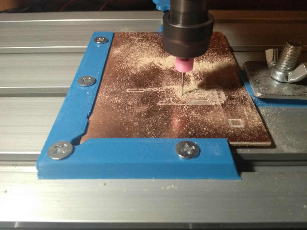
As predicted, I broke a bit, just by looking at it, it did not even arrived at the machine…
Once the probing is finished, save the height map for this job, “save as” open it and tick, “use height map”.
Test cut
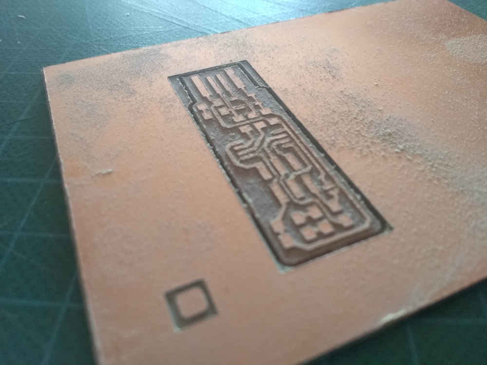
It looks like the settings are fine, maybe a little on the conservative side but it's milling well.
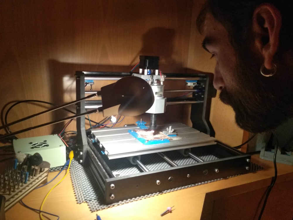
Let's go for the tracing. Making sure to reload the height map since I openned a new g.code file.
Test cut
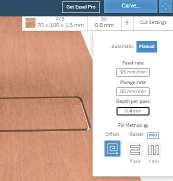
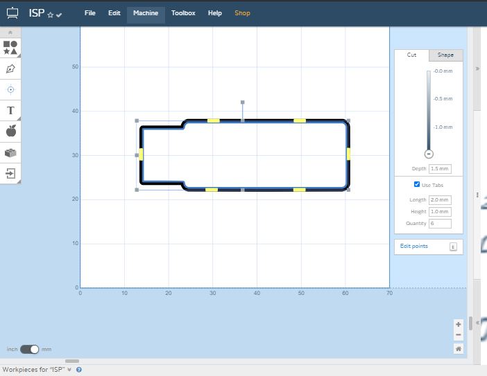
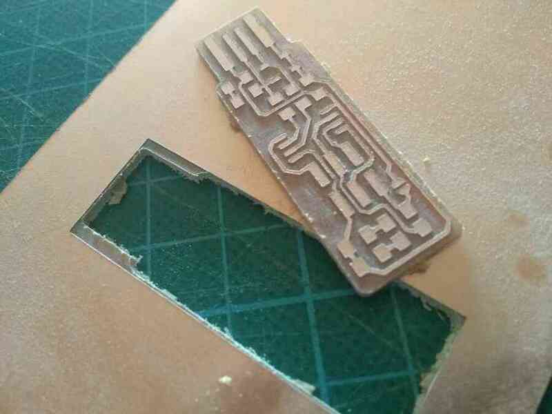
And the cutting, same process as for the tracing, but I remove the outside perimeter, as it is not needed. I am using 95mm/min feeds rate and 80 mm/min plunge rate the bit size of 0.8mm, a the depth of path of 0.4mm and added tabs.
Cutting
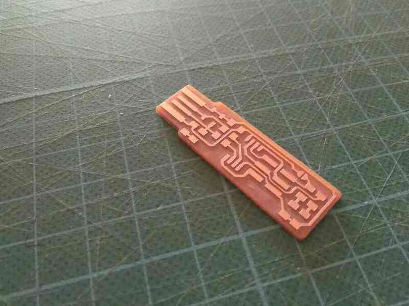
And here is the result, clip out the tabs and clean up a little...
Here is the trace test (.svg - Trace, Cut), this time with a feed rate of 150mm/min, plunge rate of 90mm/min a depth pass of 0.1mm for total depth of 0.1mm. Same for the cutting but with a depth pass of 0.4mm and total depth of 1.5mm.
Go to:Group assignment Individual assignment
Individual assignment
Make an in-circuit programmer by milling and stuffing the PCB, test it, then optionally try other PCB fabrication process.
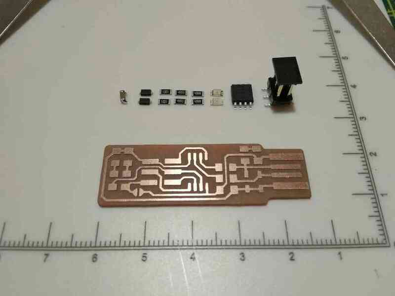
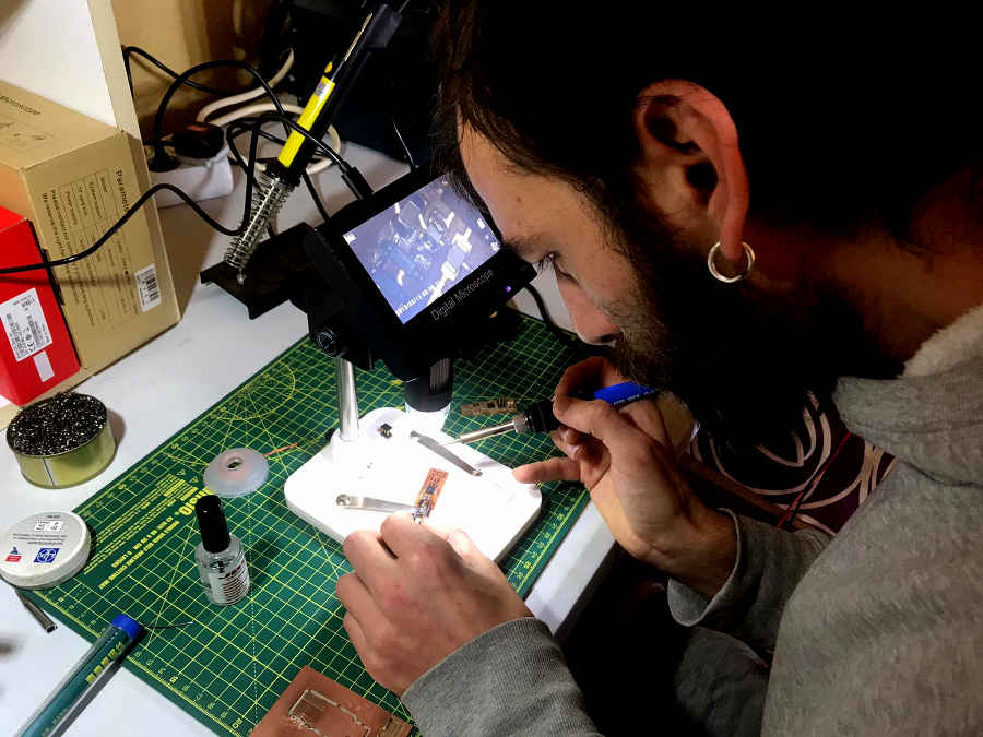
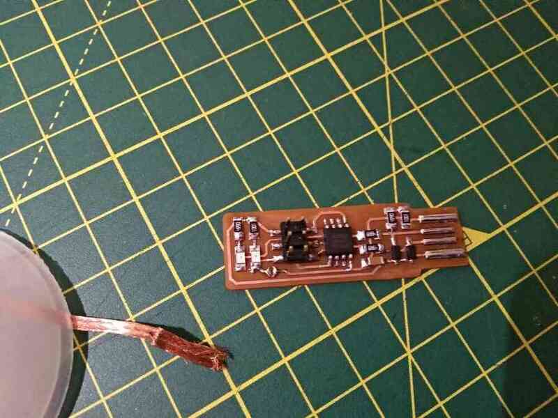
Now onto the soldering, I first need to gather the components...
Components: - 1x ATtiny45 or ATtiny85 - 2x 1kΩ resistors - 2x 499Ω resistors - 2x 49Ω resistors - 2x 3.3v zener diodes - 1x red LED - 1x green LED - 1x 100nF capacitor - 1x 2x3 pin header
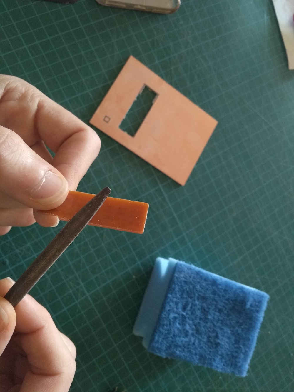
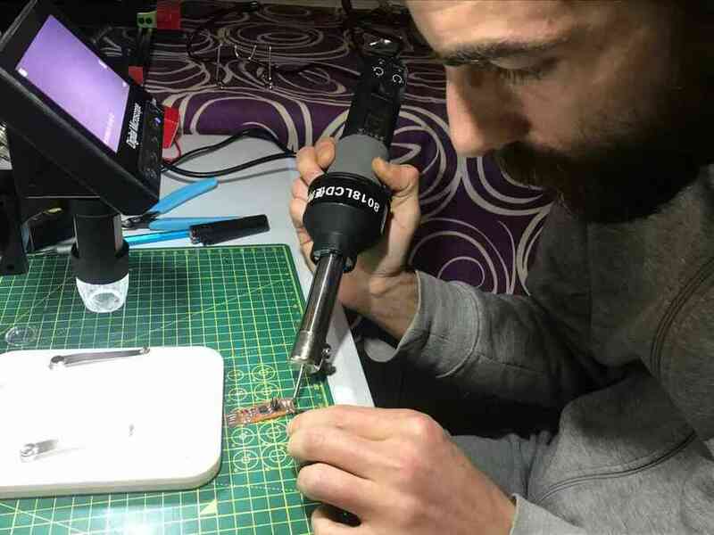
I got all the components but the CAPACITOR, I will desolder it from an extra board that was made before. I am grabbing it with the tweezers and heating the soldering points with the iron and lifting it out…
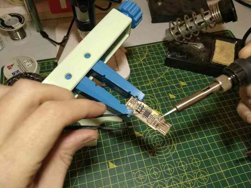
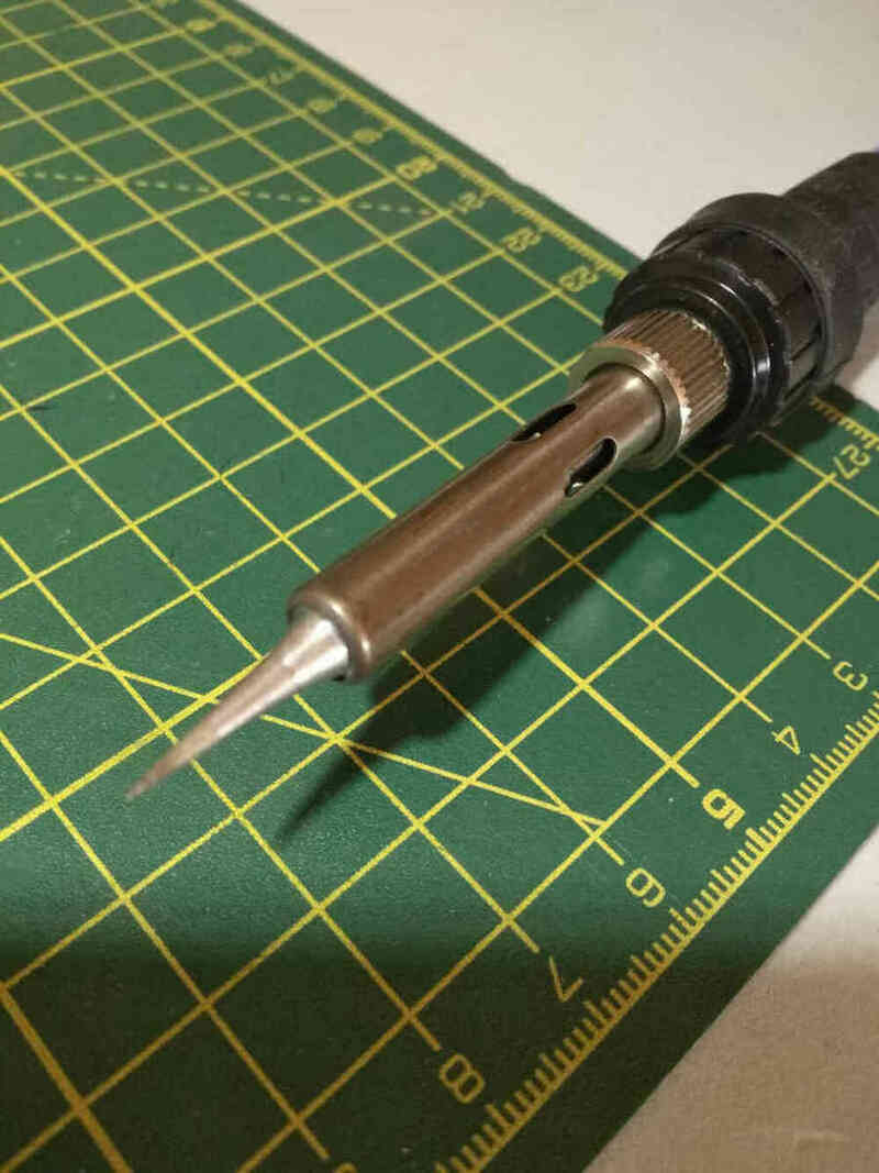
Starting with the lowest and most difficult to reach component, I worked my way through each one by one. Applying flux laying down the component, applying heat with the iron and adding solder wire.
There is 3 components that needs to be oriented correctly (polarity) as shown on the schematic below (borrowed from the documentation mentioned above)
- zener diodes are marked, both in the drawing and on the packages, with a line on the cathode side.
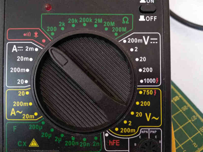
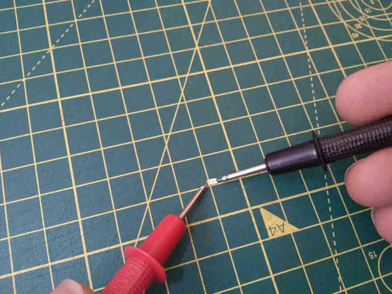
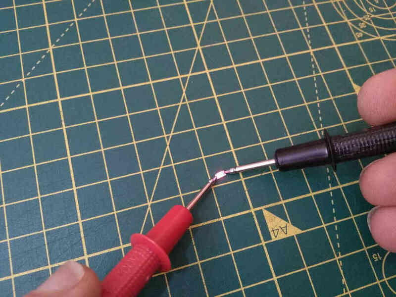
- The LEDs usually have a green or black line visible on the cathode side but it may change depending on the manufacturer. If in doubts, use the multimeter to check the polarity:
On the LED icon setting, check them with the meter probes when the LED lights up, record the polarity (red probe +, black probe -)
- The ATtiny45 marks pin 1 with a dot laser-etched into the corner of the package
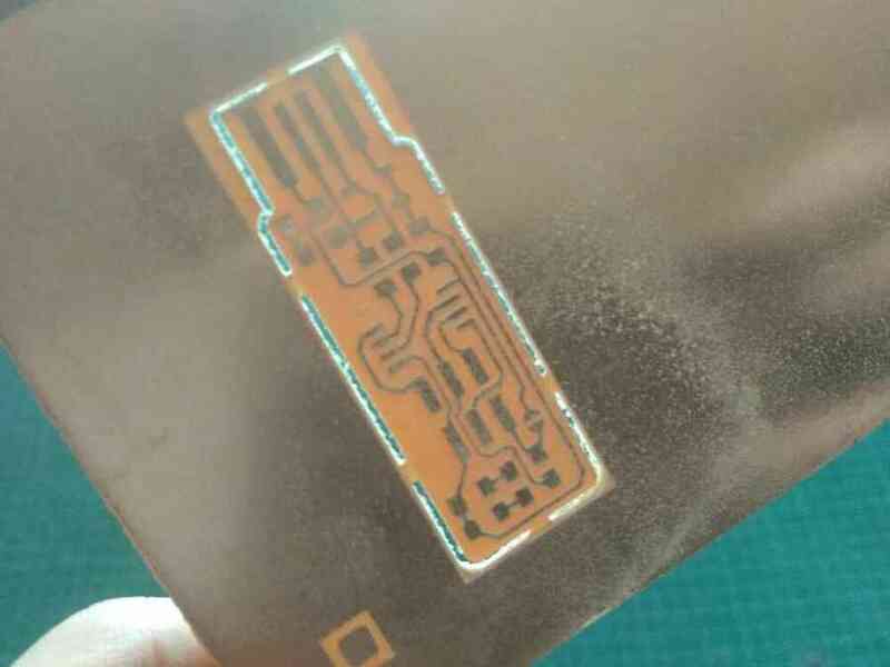
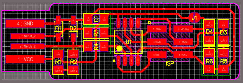
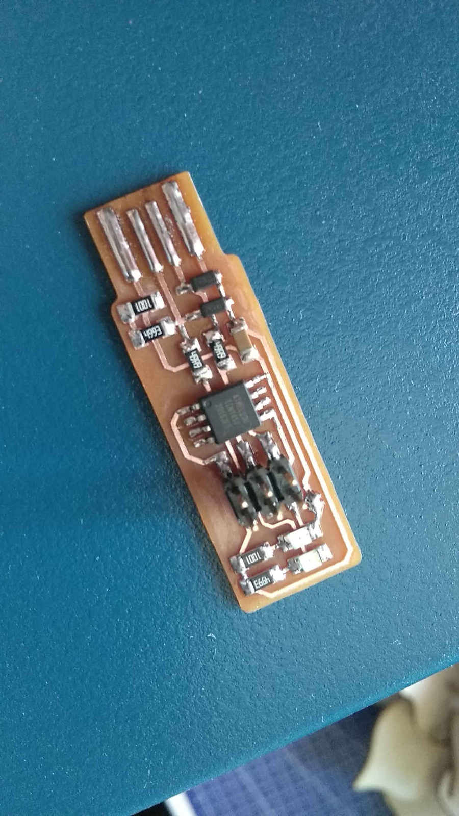
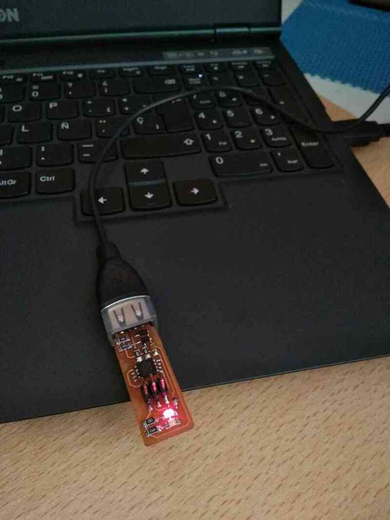
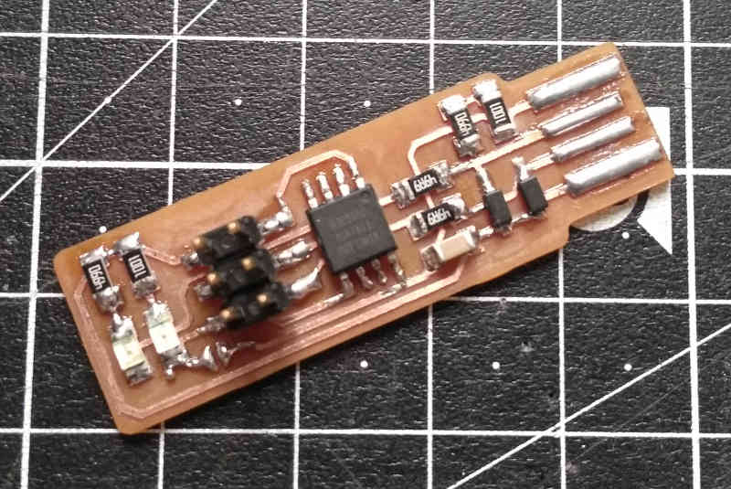
Here is the finished board, note: I added the bridge on (J1) that is needed to program it and will be removed after. Also added solder wire to thicken the USB pads and make a better connection. Check the board's layout against the schematic, looking for visual imperfections, components not lined up or not enough solder on pads and any unwanted bridge between traces.
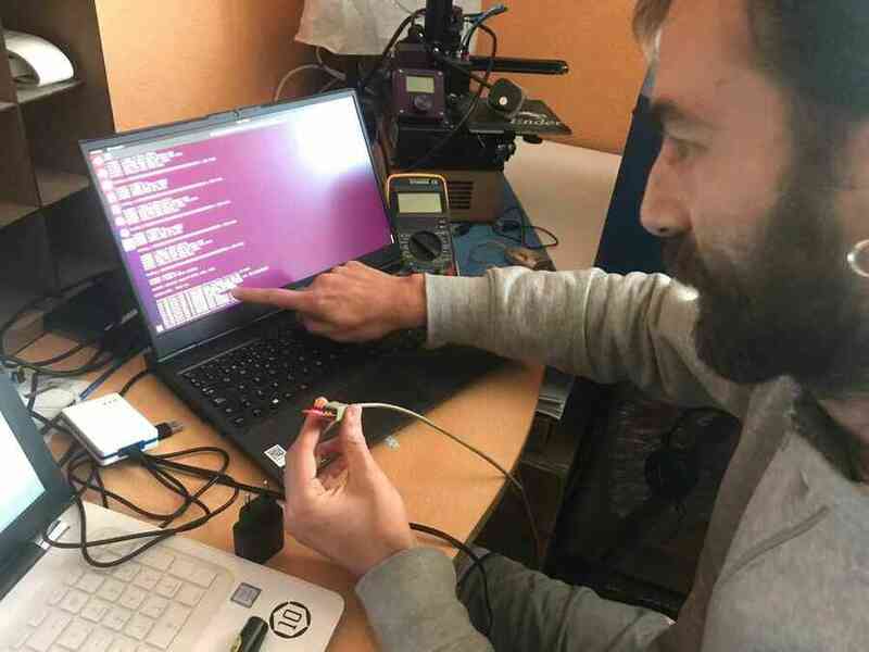
Let's program it
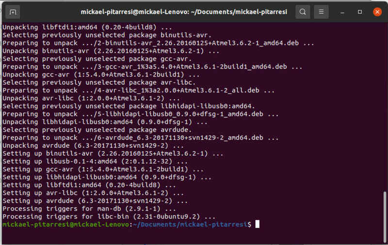
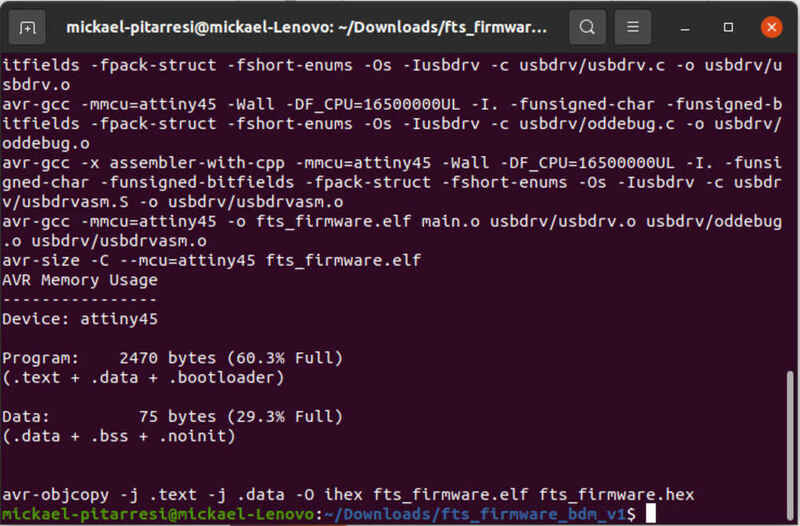
To do that I need to install the software, I will be using ubuntu and the terminal as recommended: “sudo apt install avrdude gcc-avr avr-libc make”
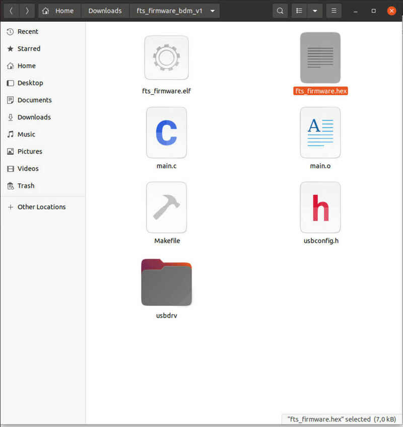
To get and build the firmware, I downloaded the source code in the class documentation, extracted the file from the zip archive, and ran “make” to create the .hex file (CD to the file location first).
Edited the makefile in Virtual studio code as I am using the atmel programer. In the file where it says PROGRAMMER ?= usbtiny I changed it to atmelice_isp, and saved the file.
Connect the board to check that the red LED is on, nice!
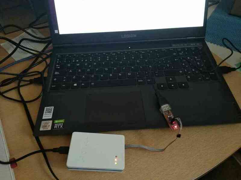
Then I connected the atmel-ICE 6 pin connector (AVR), (On the wire plastic connector, the side marked with an arrow goes to pin1).
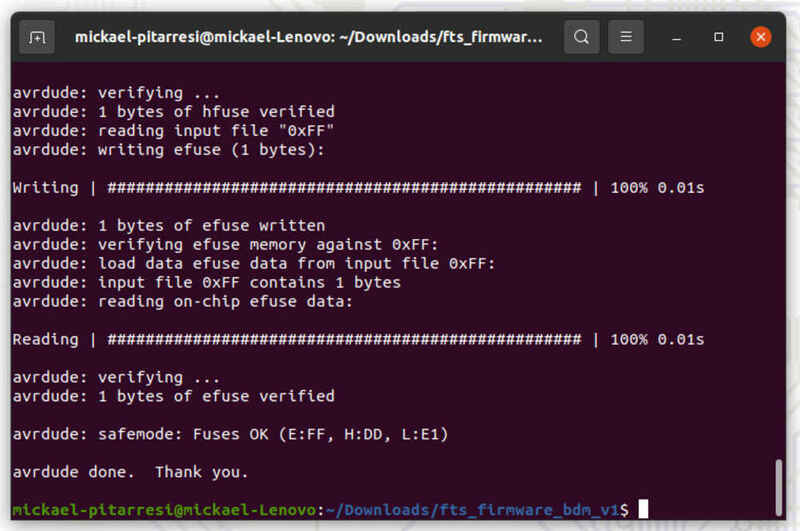
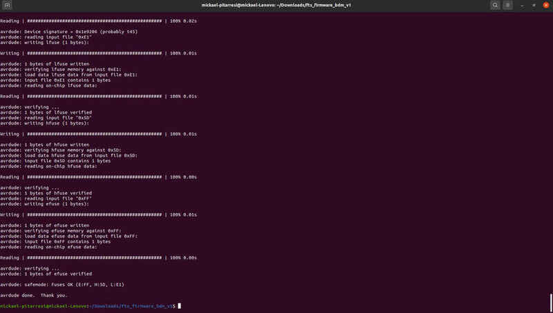
Run “make flash” to erase and flash the board and configure the fuses run “make fuses”
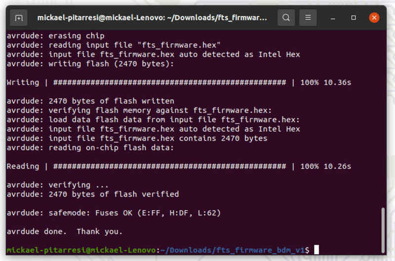
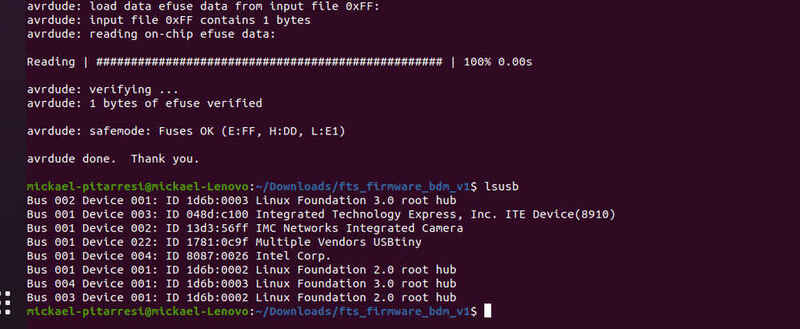
Everything looked good but when the board was reconnected, my device did not show on the list with the “lsusb” command and with the "dmesg" command, I can see an error msg...
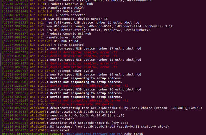
Thanks to Nuria´s eagle eyes, she spotted the mistake straight away, instead of using 499ohms resistors I used 499kohms resistors.
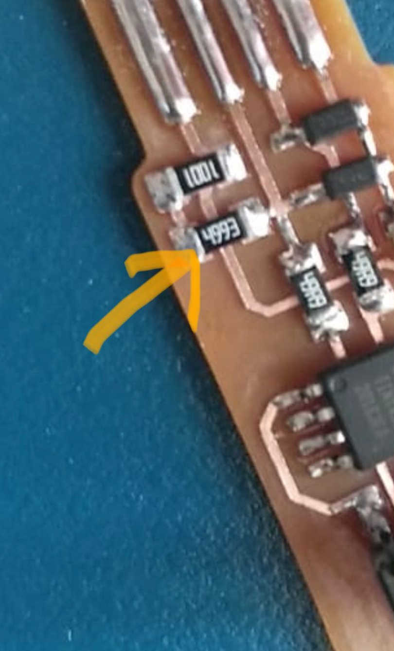
After swapping the resistor, and reprogramming the device appears in the “lsusb”!!!
I can now proceed to the blowing of the rest fuse, reconnected the board with the programmer and run “rstdisbl” which disables the reset pin and turns it into a GPIO pin.
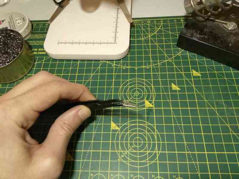
Now to remove the bridge, I try to use desoldering breads but no luck, I ended up heating the blob and dragging the excess along the trace. This helped reopen the gap.
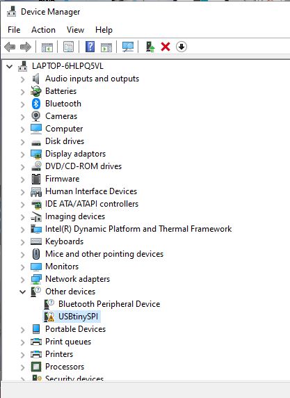
And to make sure it works, I conected it to the other computer (windows), I did not install the drivers but it does appear in the device manager.
Looks like it is working, it would be nice to try it to program an other board...
I must improve my soldering (I may be putting too much solder) and double check the components I am using. I am also redesigning the board holder so I won't be wasting so much material.
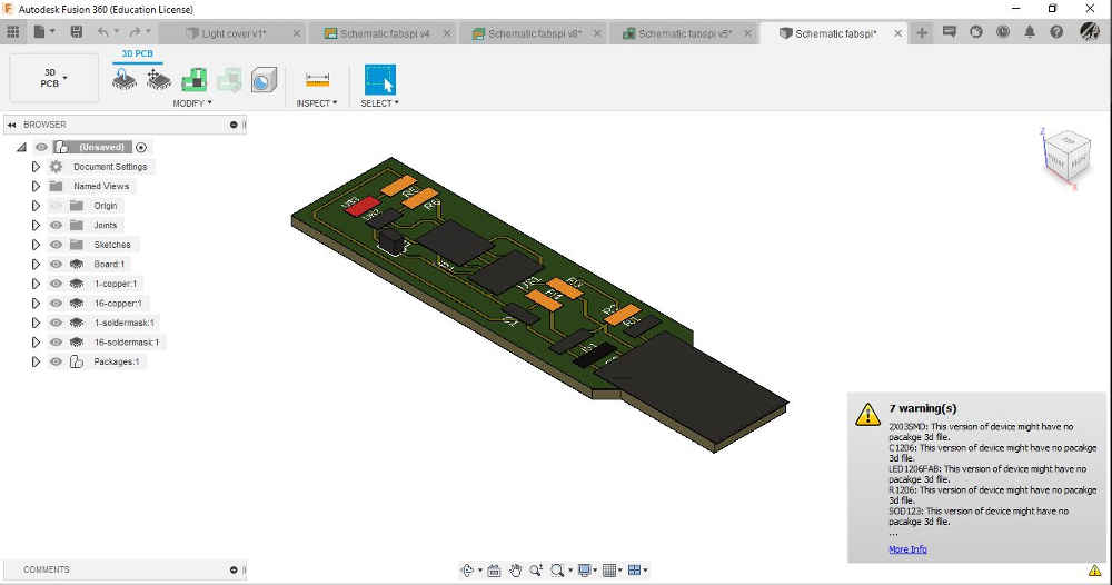
I am now looking into redoing the process but preparing the file and g-code in fusion 360.
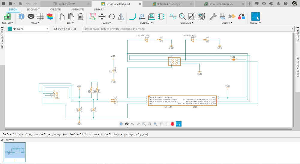
I used the schematic from the documentation and tried to find the components and libraries (not easy if you do not know the proper names…)
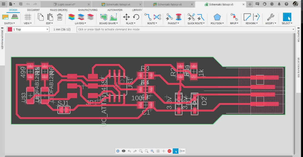
There is much to know like all the spacing and thickness of traces and pads to actually get to the milling… Here is a video showing how far I was able to go to replicate the fabisp.
I was able to find a library of components used for eagle but the 3d model (assets) are not available.
I am following this guy, he seems to have been able to get through the entire workflow.
At first I tried to use the auto trace option, but then I found myself routing it manually (I know I am not using the right usb end, but I needed something to be able to make a trace).
I have yet to get to the milling path prep, although I have done that part in the past. What really interests me is the possibility to design the electronics and the rest of the project within fusion without the need for any other design application.
Learning outcomes
Described the process of milling, stuffing, de-bugging and programmingDemonstrate correct workflows and identify areas for improvement if required
Have you?
Linked to the group assignment pageDocumented how you made (mill, stuff, solder) the boardDocumented that your board is functionalExplained any problems and how you fixed themIncluded a ‘hero shot’ of your board
Go to:Group assignment Individual assignment