4. Electronics production
Objectives
- Group assignment: Characterize the design rules for your PCB production process
- Individual assignment: Make an in-circuit programmer by milling the PCB, program it
- Optionally try other PCB processes
So this week, we started to produce some electronics, meaning that we had to “create” our boards with different processes such as CNC milling, ink deposit, chemical production, …
I learned a lot about using the CNC and the production of electronics board with it. I also learned about communication protocols and micro-controllers and how to program them.
I had some experience making my PCB using chemical processes and “industrial process” (i.e. sending the Gerber files to a production company) and how to solder both through-holes and SMD but I took the time to improve my soldering techniques.
1206 SMD seems big but is so tiny when you need to make the soldering yourself.. I feel bad for my technician at the Uni which solders 0805 every time I ask him. Thanks Jof !
Group assignment
Jason and I described the process required to mill PCBs, cover them in tin and use the voltera on the lab page.
Introduction to Electronics Production
Etching
This is the process I’m the most familiar with. Not because I’ve done it myself, but I ordered some PCBs from companies in the past and this the method they use. I gotta say, the quality of the PCBs is very good and when you need a lot of them, it’s quite cheap.
Basically, they place masks on the copper plates before etching it with an alkaline solution. The biggest drawback is the impact on the environment and staff working in factories. This is also why etching “by yourself” is usually a bad idea as you don’t have the material needed to process the waste.
I’ll reserve this process for large batches or industrial production or if you need very high precision.
At my Uni we do use quite often though but mainly due to legacy reasons. We often have some spots on the tracks where the copper was etched so we really care about making large tracks.
CNC milling
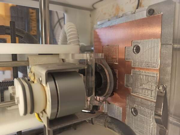
This technique consists of using a CNC to mill the copper plate. The biggest advantage is that it produces little waste and is extremely convenient for prototyping. You can have your board ready in a few hours or less directly from the Gerber to the machine without additional steps. Final good point: it can make the holes at the same time, in the same workflow ! It is however not extremely precise (highly dependent on the machine) though sufficient for most purposes and not very suitable for large quantities. It is also less practical for multi-layer boards.
The milling obviously rely on bits, and there are multiple types and sizes. At my lab we use 1/64” for tracks and 1mm for edge cutting and clearance. There are also V-bits which are cheaper but the width of the cut varies with the depth which can be inconvenient.
CNC design rules
We used this method primarily to make our board at my lab, so here are the steps required to make it work (for the Bantam tool that we have):
- Import your files. The files can be either “board” files (.brd and so on) as the Bantam software can convert these directly. Alternatively, you can directly load you Gerber files that contain all the information about your board and its layers.
- Fix the copper plate. It has to be well-fixed and as flat as possible, especially if the board is large. We use double-sided tape.
- Check the underlay of the machine. This layer is made to protect the bed of the machine and will get milled with the PCB and get scratched over time so it must be replaced from time to time.
- Zero the bit. The machine knows the height of the bed (it usually milled it itself) but it doesn’t know how far you inserted the bit. So it will measure the height of the bit relative to the bed. It does so by electrically connecting the bit and the bed and whenever the bit touches the bed, it closes the circuit and that serves as a trigger that the bit reached the bed (and it avoids breaking the very fragile bit). This must be done only once each time you change the bit.
- PCB thickness. Usually, the height of the board is known, but you don’t know the height of the double-sided tape underneath, so you must also measure the distance between the bit and the board. Same thing as before but this time the circuit is closed by connecting the board to the bed with a little metallic part. This must be done for each PCB as the board can be slightly bent or not perfectly level. This is called the “bitBreaker” utility in the software.
- Load the correct bit and settings for each bit and layer and let the machine do the work. Change the bits when requested.
Note that we use FR1 boards which is quite ductile so we don’t break our bits (industrial “green” boards are FR4 which is epoxy glass and will dull the bits).
For our mills, we use a cut speed of 200mm/minute, a plunge speed of 200mm/min a jog speed of 300mm/min and a jog height of 2mm. The spindle speed is 30,000RPM.
The cut depth using the 1/64” flat end mill is 0.08mm with 2 passes for a total of 0.15mm.
Note that since the copper is directly in contact with the humid air, it tends to oxidize over time. A good practice is therefore to either cover the tracks with solder or to cover the board in an epoxy resin or any king of protection like tin.
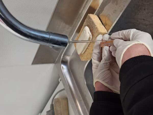
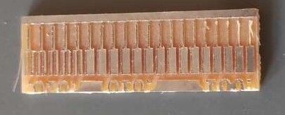
We used the files available on the fabacademy’s website to characterize the thinnest tracks we can make.
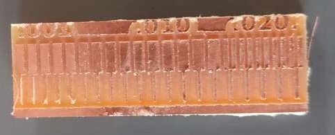
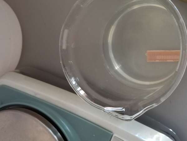
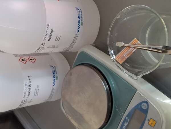
And then I covered the tracks with tin by putting the board inside a solution of tin and sulfuric acid.
Printing process
At my lab we have received a Voltera a few months ago. This a new process of making boards which involve depositing a conductive ink on a board before heating it. The machine is then able to drill the holes, apply solder paste and you just need to place the components before it heats the board and solders everything for you. The boards cost a lot more (about 5$ each) and it still requires a few hours per board.
Unfortunately, due to COVID, we didn’t really use it and bad news, the conductive ink got bad in just those few months… Anyway, we tested it in the past and here is what it is capable of doing.
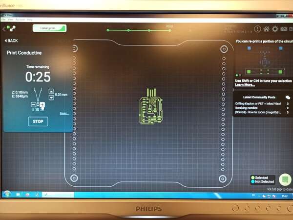
This little video shows how the ink looks like after a few months and as you can see, it is not suitable for board printing anymore.
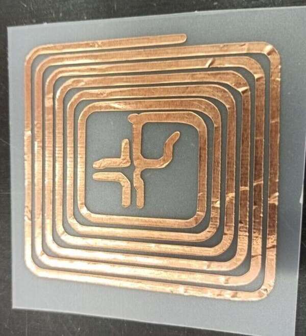
Vynil cutter
Last week I used the Vynil cutter to make a small PCB. I didn’t make any more but I think it suits this week’s assignments well so here is a pic!
Others
Laser cutting (fibre laser), printing, sewing and electro-plating are other techniques that I didn’t have time to investigate but exist !
Introduction to microcontrollers
A µ-controller is an integrated circuit (IC) that is like a very small computer, able to perform specific tasks. They are programmed to perform these tasks over and over again, on loop (but can be programmed to respond to conditions of course).
A µ-controller contains multiple parts: a processing unit of course but also some memory. This memory is either volatile: DRAM (dynamic, inexpensive and space-efficient and SRAM (static, much faster but also more expensive) that will be erased when not powered or non-volatile like EEPROM or Flash memory.
The µ-controller does not work on its own but is rather embedded and works with other components so it needs inputs and outputs (I/O) for peripheral access.
Finally, a big requirement for the µ-C to function is the clock which is sometimes provided externally and allows the µ-C to perform timer conditions.
µ-C Families
There are two main microcontroller families: the AVRs and the ARMs: AVRs are manufactured by Atmel (now Microchip) and the most common examples are the ATTiny and ATmega chips which are cheap and effective. That is somewhat of an issue as if you produce something industrially that relies on an AVR controller and Atmel stops producing them…
ARMs are produced by multiple companies and are usually used for embedded systems as they provide more features and memory than their AVRs counterparts. They are however more difficult to solder (less DIP format and usually more pins), less available in general and are usually constrained to 3.3V (requires additional converter from 5V therefore).
They both use RISC (reduced instruction set computer) instructions, meaning they require a few clock cycles (usually one) to perform an instruction but these instructions are rather primitives, allowing more space for registers.
1 2 3 4 5 6 7 8 | |
µ-C programming
As said before, µ-C can perform specific tasks like switching an LED on or off or actuating some servo-motors. To specify these tasks, the µ-C needs to be programmed.
To be programmed, a µ-c must first be loaded with a bootloader, i.e. a small piece of code that can reprogram the rest of the memory based on what is sent to the µ-C and is interpreted by the bootloader. At reset, it’s the bootloader that runs first and has a look at the programming port to either reprogram the rest of the memory or jump directly to the programmed main code. Then, code can be sent to program the µ-C the way you want it.
AVR
AVRs are programmed using ISP (in-system programming), PDI (Program and Debug Interface) or UPDI (unified Program and Debug Interface). The latter is the one used on newer AVR devices and consists in a one-wire interface.
ARM
ARMs are programmed using either a JTAG (Joint test Action Group, the group who designed the standard) interface or a SWD (Serial Wire Debug) interface.
JTAG uses 5 pins: clock, mode select, data-in, data-out and reset. It can be reduced to only serial data and clock.
SWD is an implementation of JTAG for ARM processors and consists of simply two pins: data and clock (SDIO and SDCLK) along with VDD and GND obviously and an optional reset.
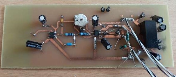
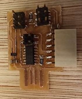
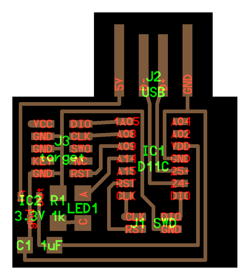
First board: AVR programming board (using SAMD11)
The first board is a programmer (or rather a USB-UPDI converter) board for AVR device. I used my instructor Quentin‘s board. It is very minimalist and does the work flawlessly.
So the idea here is to use an ARM board (SAMD11) to convert USB (serial emulation) data to UPDI so that we can use this to program AVR (Atmel, like ATTiny ou ATMega) µ-controllers.
The board is rather simple:
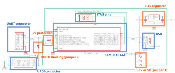
It uses the USB 5V and a 5V-3.3V converter to power the ATSAMD11 and consists of a reduced-JTAG connection (Clock, data, VDD, GND) to first install the bootloader and will be able to convert Serial to UPDI or UART based on the jumper selection and can provide 5V or 3.3V to the AVR device. Some protection resistors limit the current.
The board has been manufactured using the CNC milling machine described before. I used a 1/64” flat mill for accurate traces and a 1mm flat mill for cutting the edges of the board and increase the clearance between the tracks.
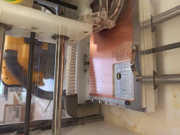
It was then time to solder the components on it. Nothing too difficult as I’m used to soldering still 1206 SMD is tiny so it’s always a bit challenging!
The Bootloader
Time to install the bootloader on the SAMD11 ! Because the SAMD11 is powered (5V) from the USB, it has to be connected. At that time I noticed two things. First, the board is too thin to sit tight in an USB port… So I added extra duct tape under it to make it bigger (real tinkering there !) Second, I must have done a mistake in the CNC file because the board edges were a bit too big… Time to file the excess to make it fit the USB port !
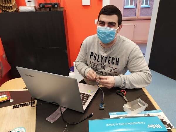
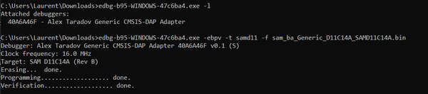
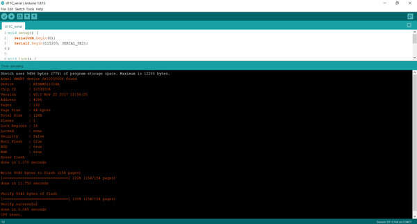
Then I used my instructor’s own programmer to program my board (after an initial struggle with another one, see below). Plugged his board’s USB into my computer along my own board (for the 5V). finally, I connected the JTAG from his board to mine. The SAMD11 is filled with a bootloader (sam_ba_Generic_D11C14A_SAMD11C14A.bin) and I downloaded edbg, a CMSIS-DAP programmer that is used with the command line. Linux is cool for that… You can easily check if your USB port is working and what is connected to it. Moreover, edbg is easier to use once compiled on a Linux machine. Anyway, I succeeded with Windows eventually but that was a bit harder.
First, I connected the programmer and I could find it with edbg. Then I wanted to try and erase the memory of my chip using the -e flag. That’s when I realized I had to find the exact name for my SAM target (which is samd11).
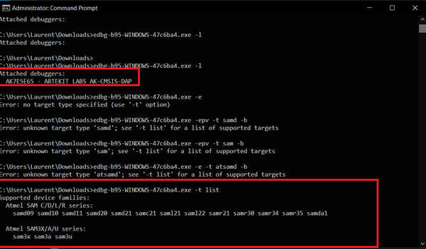
Unfortunately, I initially couldn’t make it work. It is probably the programmer that I first used and the fact that my USB ports did not always respond immediately.
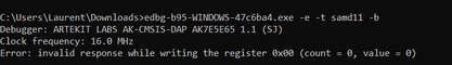
I then changed it for my instructor’s programmer and it went through successfully.
edbg-b95-WINDOWS-47c6ba4.exe -ebpv -t samd11 -f sam_ba_Generic_D11C14A_SAMD11C14A.bin
USB-UPDI converter
Once done, we can use the Arduino IDE and some libraries to program the SAMD11 using the USB port since a bootloader is now present.
I installed the Arduino core for SAMD board into Arduino. First, I tried to install those that are natively available in the board manager (SAMD Core) but I couldn’t compile my test code.
I then looked up online only to find a fork of this core for the exact bootloader that I loaded; Arduino Core.
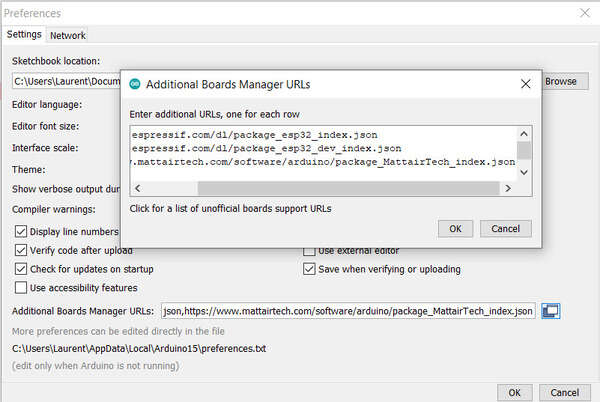
The procedure to install it on Arduino is as follows: First, add the JSON index of the core into the board manager (preferences menu)
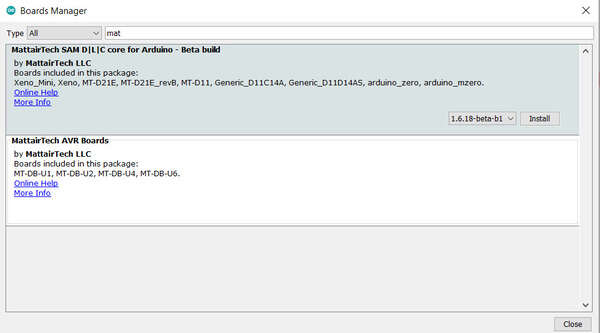
Then open the board manager and look for the mattairTech SAM D Core.
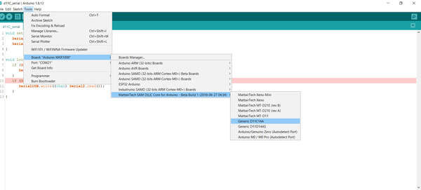
Once installed, select the correct COM port on which the board is connected and make sure to choose the correct board (Generic D11C14A):
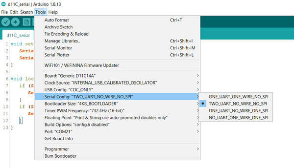
Finally, make sure to change the Serial config:
We can now start to program our board with the code we want. In this particular case, because we want to convert Serial to UPDI, we simply ask the chip to convert USB data (if data is awaiting on the serial/USB bus) to UPDI (then write it on the UPDI port) or the inverse (if data is received on the UPDI end, then write the data on the Serial port).
1 2 3 4 5 6 7 8 9 10 11 12 13 | |
Our programmer is ready to… Program !
I then tried to install Quentin‘s new version of the code. It is basically the same as above but dynamically detect the baud rate.
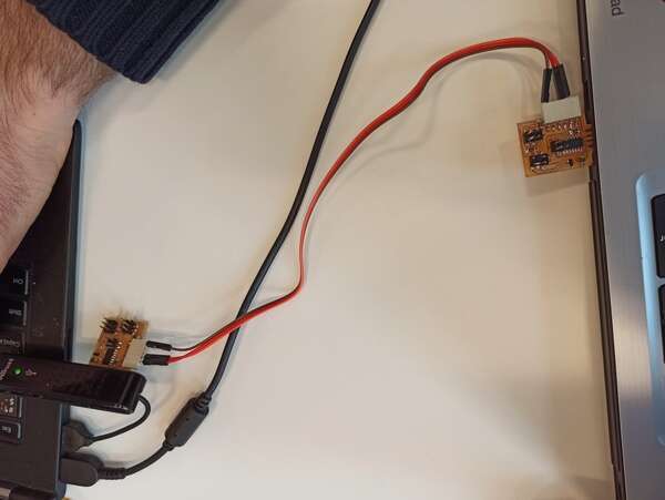
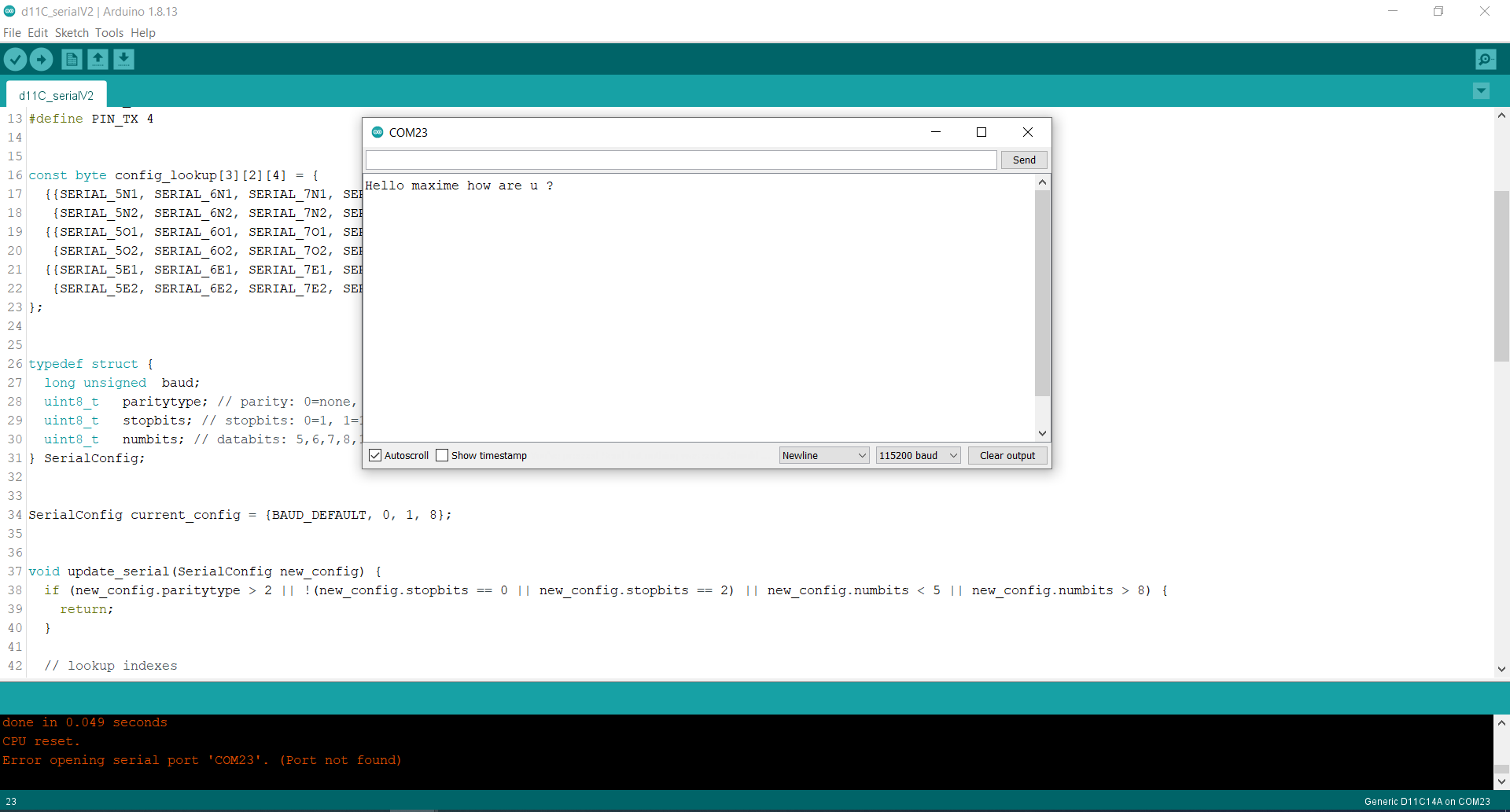
I could connect Jason’s board and mine together through UART protocol (RX and TX opposed on each board) and we could communicate through our own serial monitors in Arduino IDE !
Second board: ARM programmer
The second board must act as an ARM programmer. Note that we should have done the reverse (this board first) so that we can use our own board to program the AVR programmer.
For the second board, no Gerber files were provided so I had to use mods to create the Gcode from the image (png) file. This is possible because png is lossless and the dpi (dot per inch) is known. Neil’s files are at 10000dpi.
I chose the CMSIS-DAP.4.D11C board as it has an LED but is otherwise quite minimalist:

I used mods (right-click - open server program - 2D PCB png) to create the GCode.
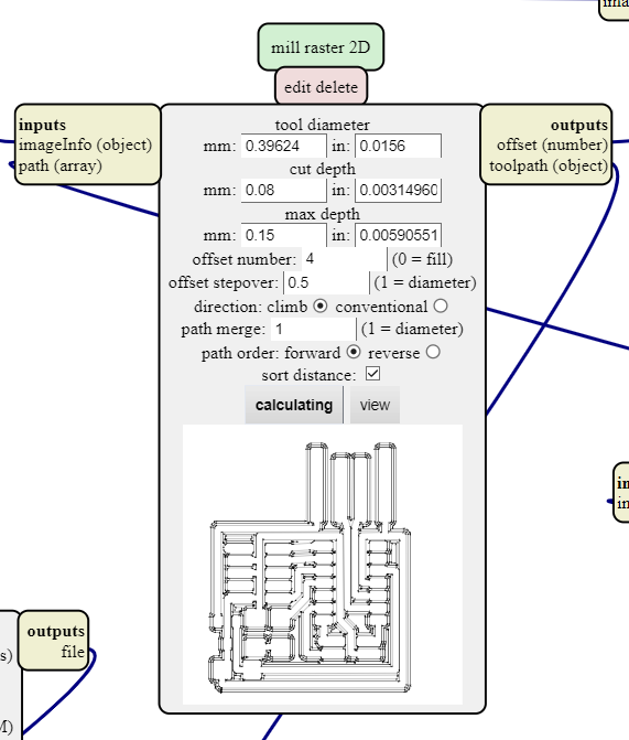
First, I load my traces png, set the tool diameter, the cut depth and the offset number (the number of semi-overlapping pass to increase the clearance).
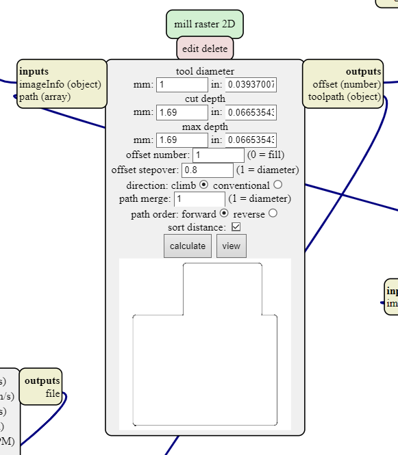
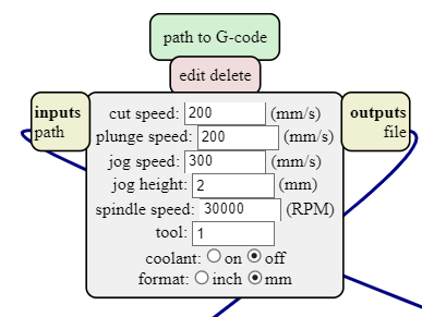
Then I change the milling parameters:
When clicking on “calculating” I can save the .nc (gcode) output file.
Note however that Bantam tools does not handle G54 coordinates system ! It must therefore be removed from the output file ! Else, I could also modify the script in mods and save the whole program to later locally load it if I need it again.
For the outline, the process is the same but the tool parameters are obviously different.
An alternative to mods would be Flatcam but I didn’t have the opportunity to test it.
Unfortunately, I had some issues as the bits I used were a bit dull as it can be seen on the traces :
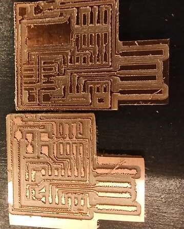
That lead to difficult soldering.
Also, I had trouble installing the bootloader (free_dap_d11c_mini). This is probably because I only had an Atmel ICE available and I had trouble finding the right pins and how to make it work. In the end I think it didn’t work because I didn’t connect the VCC to my board voltage as I thought it was to power it but I supply it with the USB so I though it was not necessary.
To go further
I would like to use the CNC milling to make USB keys and an AVR controller to be able to… do things. I don’t know what yet but I’m sure I’ll find more ideas. I could use a 3D-printer to make a small case for it, maybe some epoxy resin to protect the circuit…
It would be nice to test laser cutting (fibre laser), printing, sewing and electro-plating to make PCBs in the future !