8. Embedded Programming
Objectives
- Group assignment: Compare the performance and development workflows for other architectures.
- Read a microcontroller data sheet.
- Program your board to do something
Group assignment
See our group page.
Introduction
Since I already did some embedded programming in the past week:
- Making a programmer which is basically a Serial to UPDI converter
 1
 2
 3
 4
 5
 6
 7
 8
 9
10
11
12
13
void setup() {
   SerialUSB.begin(0);
   Serial2.begin(115200, SERIAL_8E2);
}

void loop() {
   if (SerialUSB.available()) {
      Serial2.write((char) SerialUSB.read());
   }
   if (Serial2.available()) {
      SerialUSB.write((char) Serial2.read());
   }
}
- …
I decided to have a try with something I am not really comfortable with: FPGAs and try to get a clear enough documentation for anyone who would like to get started a starting point.
FPGAs and Hardware Design Introduction
Nicolas, one of my instructor recently bought an ICEStick, a development board for a Lattice ICE40 FPGA. He will try to use it by installing a toolchain on Linux (will post a link to his documentation when he’s done) while I’ll try to do the same but for Windows.
Usually, it’s better to stick with the manufacturer’s toolchain to make sure all features are available and there will be no issue but in this particular case, some people have reverse-engineered the ICE40 board: Project ICESTORM so they can analyze the design and create correct bitstream file to “program” the FPGA. This the way to go if you want to use free, open-source software.
In my case, I will use the Lattice Software (see below).
Before actually “programming” (you’ll see the reason for the quotes below), there are three steps (for me) that you need to do before:
1. Understanding Hardware Logic and Designing
I will go deeper a bit below, but hardware design is completely different than designing software. You need to take this into account and avoid the bad habits that we are used to in classical programming. There is no better way than simply studying the theory behind.
2. Play with a simulator
Though I won’t go into the details here, I highly recommend playing with simulators like Icarus, ghdl or logisim to get an idea of how to conceive your design and understand the basic rules of hardware design.
3. Language: Verilog VS VHDL
The third step before getting into action is to choose the language you’re going to use.
Verilog and VHDL are both hardware design languages (in fact VHDL = VHSIC Hardware Design Language, VHSIC = Very High Speed Integrated Circuit). Both are used in the industry and in research and have their pros and cons. VHDL is based on ADA and Pascal syntax. It is extremely typed, deterministic and verbose. It therefore has better verification features and it is harder to make design mistakes as a beginner as the compiler will not allow it. Verilog is supposedly easier to learn and gives results quicker (less typing required). It is quite similar to C. But since it is not as verbose, it is (though very rarely) sometimes not deterministic (see non-blocking assignments in Verilog) and will allow error at compilation.
Anyway, there is no bad choice here, simply pick your poison 
Introduction to Hardware Design
So I looked up online to find resources and understand what this is all about. This section will be a summary of what I learnt and what is (for me) important in the design (most illustrations come from courses of Prof. Dragomir Milojevic).
What are FPGAs
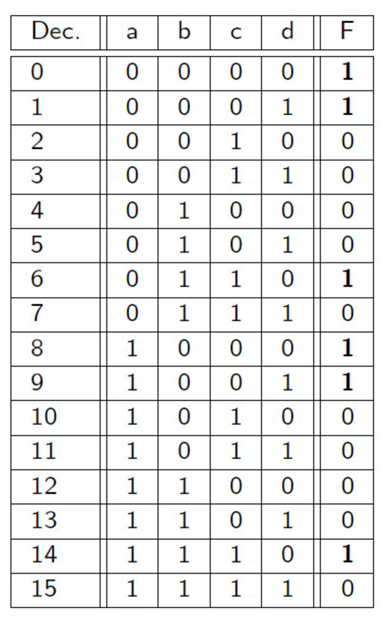
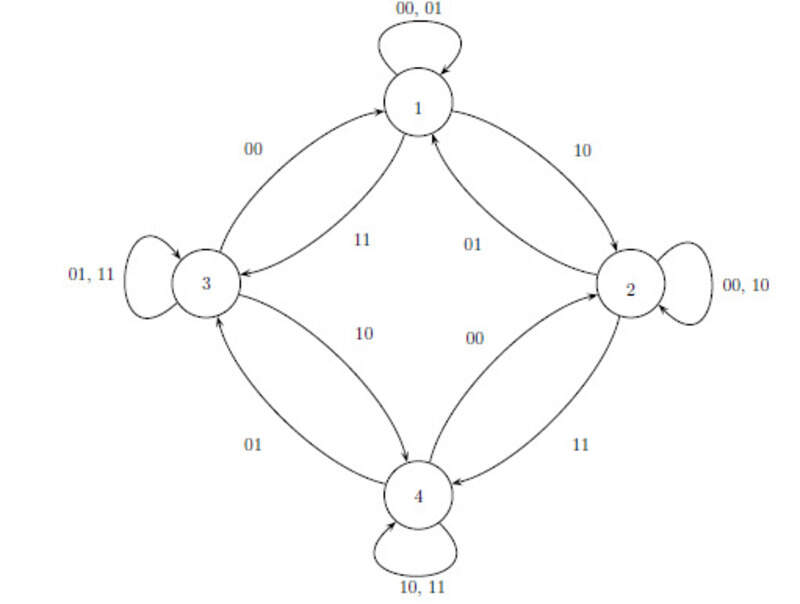
Logic circuits whether combinatorial or sequential are a way to represent logic functions. Reminder: logic circuits = systems that process digital information using boolean logic functions implemented in hardware. Inputs (+internal states) produce a specific output and a new system state. Combinatorial circuits use logic gates and look-up tables (LUTs) while sequential circuits also use the actual state of the system to decide of the output and can be synchronous or asynchronous.

Logic optimization
However, this kind of table or minterm is not optimal in terms of gate counts and it is important to save resources (power, space, cost, … ). This creates the need to optimize the logic function.
Multiple optimization methods exist: Karnaugh maps, Quine-McCluskey, … but they all become difficult to use and compte “by hand” when we have more than a couple of state and input variables.
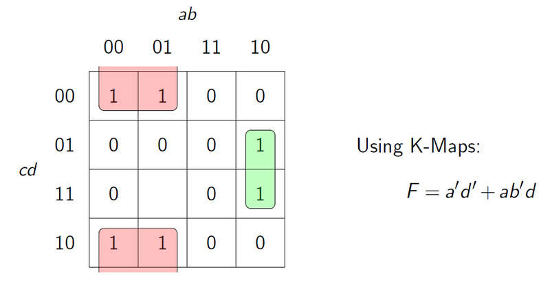
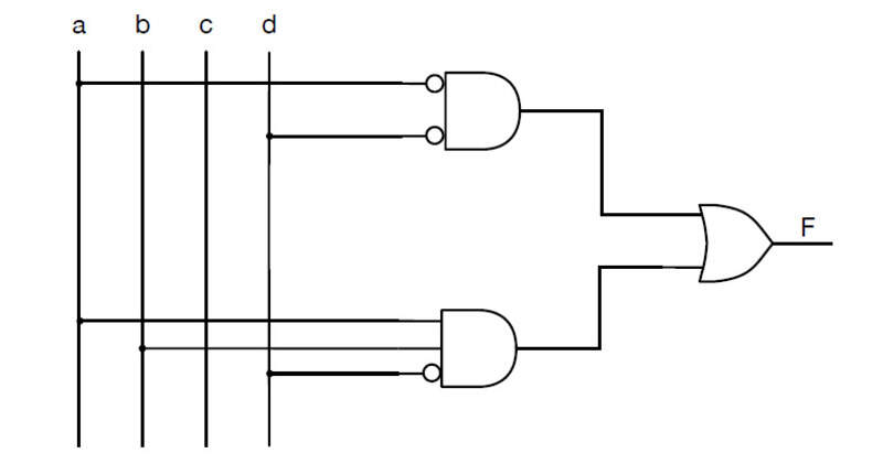
In the end, we can obtain what we call a Sum of Products (SoP) that is easily implementable in a logic circuit in a recofnizable pattern. Indeed, a sum is nothing than an OR gate and a product is an AND gate. That means that a SoP is a couple of parallel OR gates connected to a final AND gate.
Hardware design
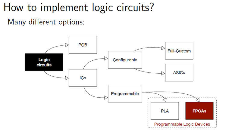
When it comes to electronics design, PCB are just one of the way to go. In fact, when you really need to work with combinational logic (meaning, thousands of logic gates), it makes sense to use integrated circuits. They can be configurable (full-custom and application specific IC (or ASIC)) or (re)programmablem: Programmable Logic Array (PLAs) and Field Programmable Gate Array (FPGAs).
To design a digital system like these, you need to rely on hardware modeling languages as it would be inconceivable to do this by hand. LC design = use verbal, formal specifications to create a circuit, down to the information required to manufacture it and physically implement the functionality. The logic can be optimized by different algorithms to reach either performance, power or area optimal logic circuits.
Hardware designing languages are nothing but a way to describe, optimize and implement logic circuits.
Design flow
Design a logic circuit should follow these steps: 1. Define the systems specifications (high-level) 2. Establishment of the formal specifications in the HDL model 3. Simulation 4. Synthesis: transformation of the HDL description into a gate-level netlist 5. Placement and routing: placement of components (if needed) and routing between them
Using FPGAs, we won’t need to bother much about the steps 4 and 5 as tools are there to do them for us. Step 3 should usually always be done but I didn’t really have time to get into this week. So I’ll focus on step 2 mainly so that you know how to write (a bit) HDL code.
As stated before, a Sum of Products can be expressed as parallel OR gates and finals AND gates. This is exactly what happens during the Placement and routing step in a PLA (Programmable logic array):
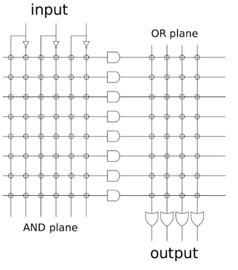
This is however quite limited in terms of I/O.
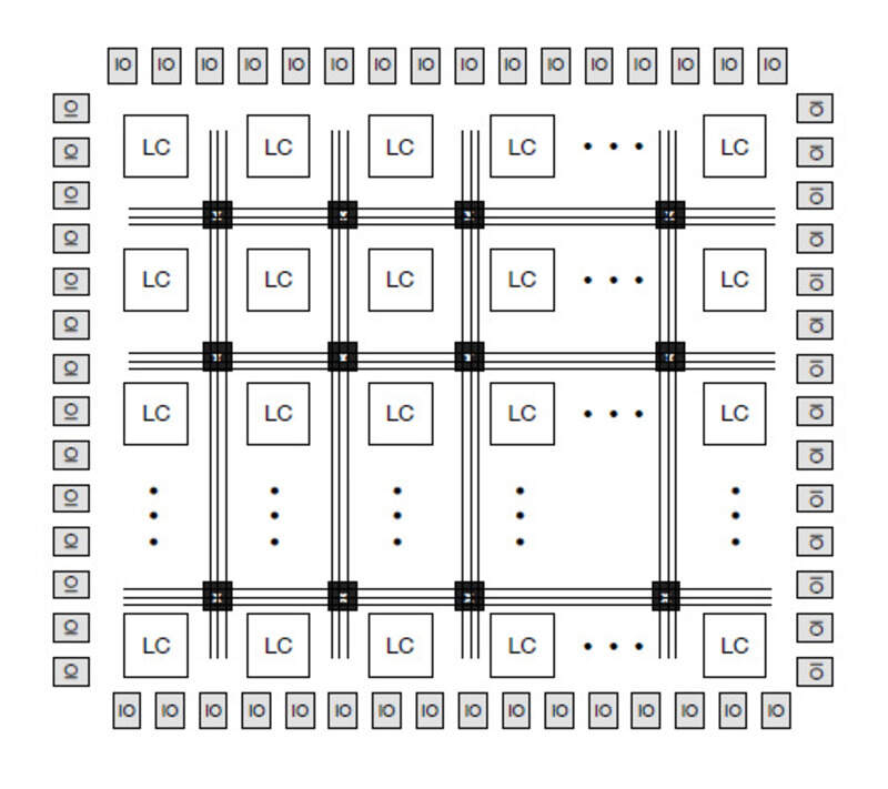
FPGAs rely on Logic Cells to implement logic functions (memories with LUTs) and interconnections, IOs, CPUs, …
Syntax
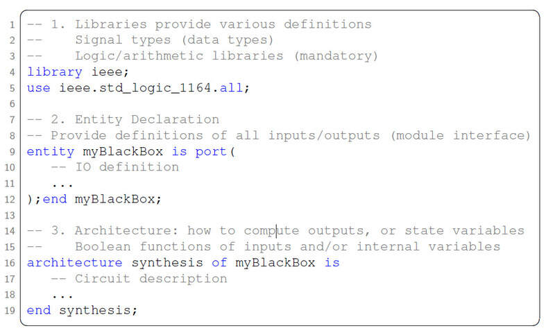
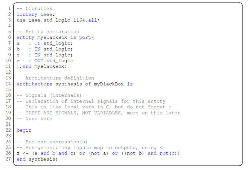
HDL relies on modules, entities or architectures. Meaning blocks that have inputs and outputs and perform some kind of logic function. We will therefore always define some modules, its ports, and its implementation (i.e. what it does and whether it is purely combinatorial or sequential).
1. The basics
- Identifiers are not case-sensitive and can start with a letter (1abc = 1AbC).
- Numbers can be set in various base
- HDKL is strongly typed as there can be no ambiguity on the type of your identifiers as it will impact the physical design.
- Always use an assignment (value <= 3). This is like soldering a wire between two points.
- There is no “sequence” in your assignments, this is different than in a programming language ! Everything happens at the same time, but be careful of race conditions !
- All logic operators can be used (AND, OR, XOR, NAND, NOR, XNOR, NOT) as well as arithmetic operators (+,-,*,/)
- Libraries can be added to your design.
- Do not drive the same wire with different expression (tmp <= a, tmp <= b). That would create a voltage divider.
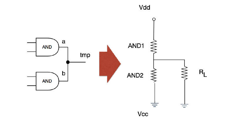
- This would work in simulation due to the computers being sequential ! It is not because your simulation is working that the circuit will work
Example in VHDL:
2. A bit less Basic
- Never place an output on the right-hand side of an assignment as it would mean a feedback on the signal ! This would create a sequential but asynchronous circuit that is subject to race conditions and may not operate correctly. This is completely different than with a classical programming language.
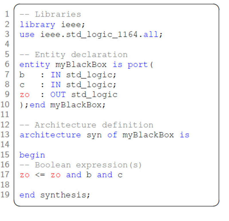
- To avoid this, we need some kind of synchronization : the clock.
- A synchronous circuit must be inside a “process” in VHDL or inside an “always @ xx” in Verilog.
- This kind of process will instantiate a D-flip-flop during synthesis (on the rising edge, will store the value on the input which will be kept there until the next rising edge).
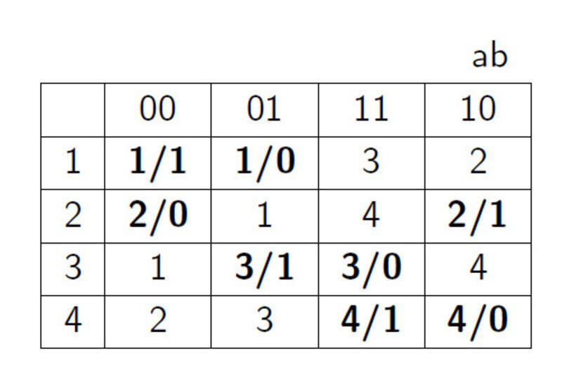
3. Implementing truth tables
You can implement truth tables by hand (using the minterm expression for example) OR you can use the select identifier. This allows a direct encoding of the truth table and the logic function synthesis and optimization will be performed automatically.
4. If and loops
-
If statements will, in hardware, instantiate a multiplexer. You need to cover every possible outcome with elseif and else conditions, otherwise, the system will infer a latch to store the value. Not only will the timing be different but you add another component (area, power, cost) and this will add a complete additional cycle to your logic !
-
The only valid loop is the for loop. It will physically instantiate repetitions of the design in series, this is why while loops cannot be instantiated (works in simulation though).
- In classical programming the loop index is a variable that can be assigned. Not here ! The loop index is not solved dynamically, you just progress in the physical design in series.
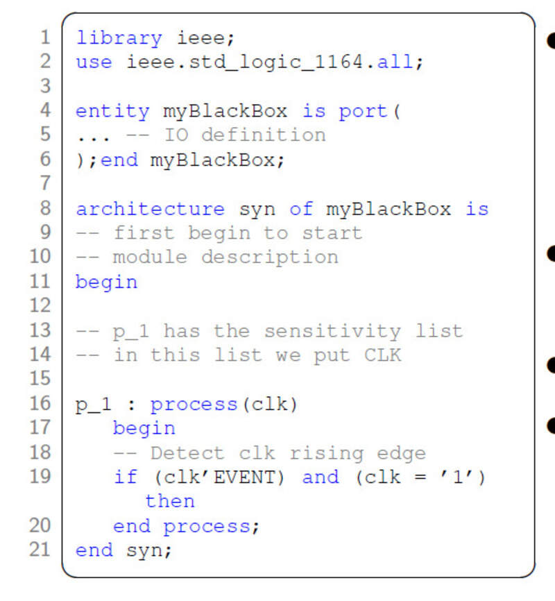
5. Reset
You need to use the reset of your board. Most boards feature a reset on configuration (RoC) or Power On Reset (POR). Some boards will allow to set initial registers based on this, other just to set the signals to zero (it is note because it works in simulation that it will work in the circuit).
In a process, you should always check the the reset and then the rising edge of the clock.
6. Do’s and Dont’s
In recap:
- Use signals (not variables)
- Use processes for use of a clock (synchronous)
- A process is in the form of
if(reset) signals <= 0 elseif (rising_edge(clk)) do_smthg - Subdivide the design in modules
- Instantiate the signals and outputs to zero at reset
- Different processes can see all signals but only one process can modify a given signal.
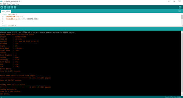
Installing the toolchain (Windows, proprietary: Lattice)
Some will argue, saying there is nothing better than open-source, but when dealing with FPGAs, I always prefer to go with the manufacturer’s toolchain. In this case, the manufacturer is Lattice. The toolchain is available on both Windows and Linux.
1. Synthesizer
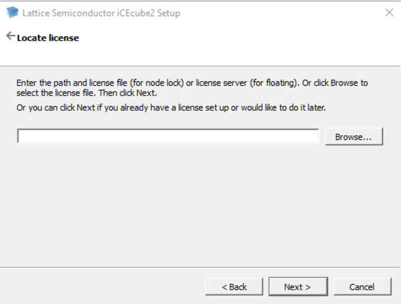
- The first step is to install Lattice IceCube2. You will need to make a new account and download the executable to install the software.
- You will also need a license (free !)
- When asking for a license, you will need to provide the MAC address of the computer you intend to work on (yeah, not very friendly…). Open a (Windows) terminal and use the
ipconfig/allcommand to retrieve your physical MAC address:

- You will then receive an email with a
license.datfile. Download it and store it carefully. - During the installation, the software will ask for that license file. Browse and locate your file.
- Install the core tools and open the software
This software will allow to compile your Verilog or VHDL file and create the netlist based on your verbal design. It will then, based on constraints, make the placement and routing of your logic gates. All of this will be compiled into a .bin bitstream file.
Info
This is not a text/code editor ! You will need to manually create and edit your design files in another editor (I personally use Notepad++)
2. Setting up a new project
First, grab the datasheet of your board and the pin list: ICE40 datasheet, ICEStick evaluation board manual.
You can then create a new project in ICECube2. Make sure to select the correct device family and package. In this case, we have an ICE40 HX1K (1024 logic cells) in the TQ144 package. Make sure to select also the 3.3V voltage for the four IO banks of the FPGA. If unsure, check the datasheet !
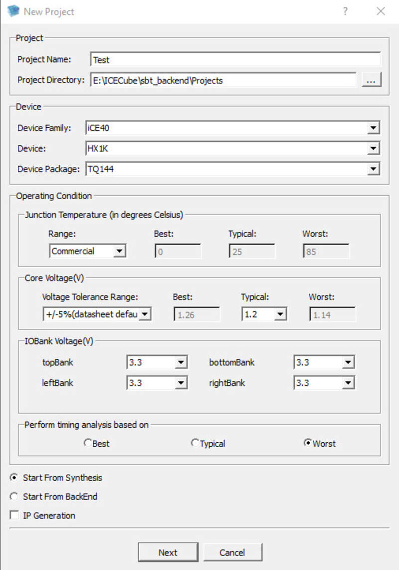
You will then be able to add your design and constraints files from the menu on the left and run the synthesis and placement&routing tools.
3. Programmer
You will then need another software to upload the generated bitstream to your board. Again, the lattice toolchain, for the ICE40 boards, provides the Lattice Diamond Programmer.
Once installed, you can create a new project. If your FPGA is plugged in, you can try to scan it to detect the correct device.
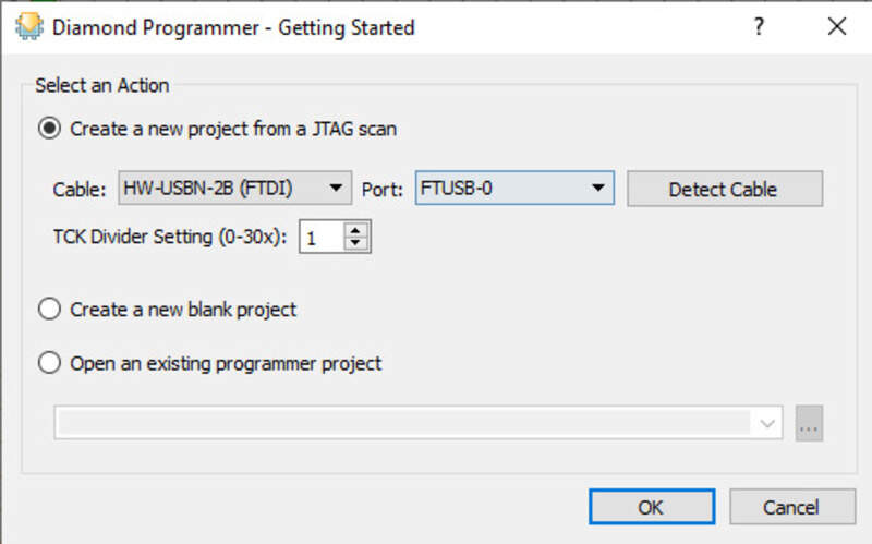
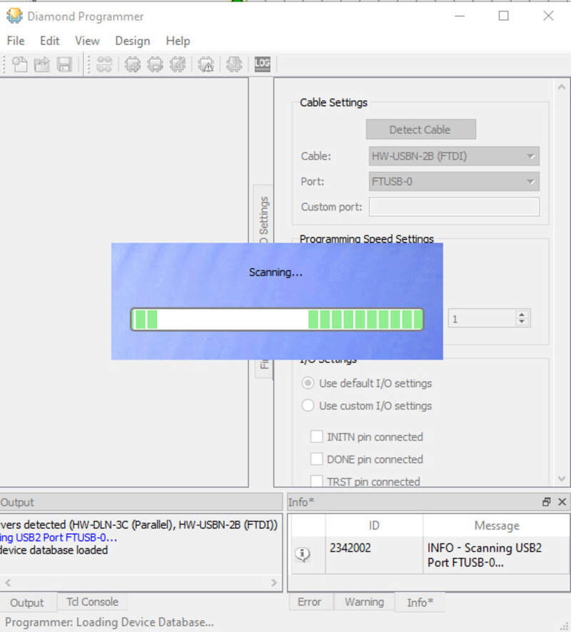
It will probably fail, in which case, no worries we’ll edit the correct device right after.
4. Testing the toolchain
The manufacturer provides a working/test/example bitstream (in the downloads tab) to upload.
When downloaded, edit the device settings:
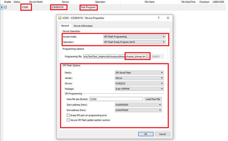
Make sure to select the ICE40 device family, ICE40HX1K device and the fast program operation. In the pop-up window, select SPI Flash Programming and select the bitstream file.
Danger
Do NOT select NVCM (non-volatile) as it is a one-time, irreversible programming ! Only use it in production once your design is finished.
The question is then: what SPI options do we use ? If in doubt: check your datasheet
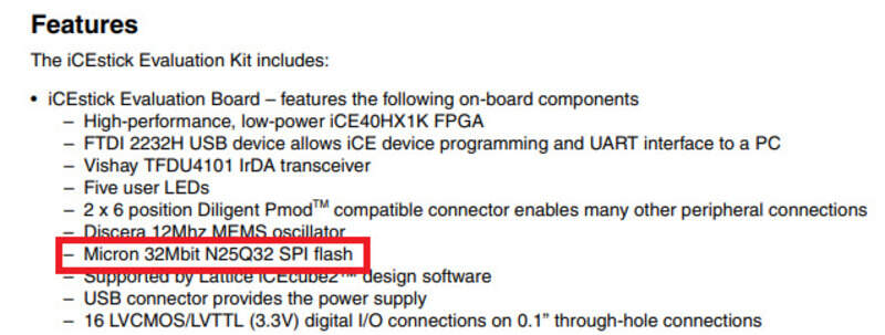
The datasheet indicates the Micron N25Q32 device for SPI programming. Note that it is an 8-pin VDFPN8 package (I didn’t find it in the datasheet so I checked physically on the board with my eyes!)
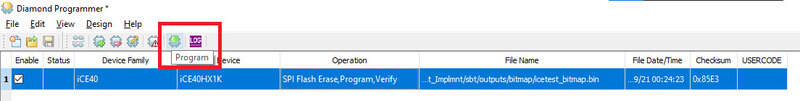
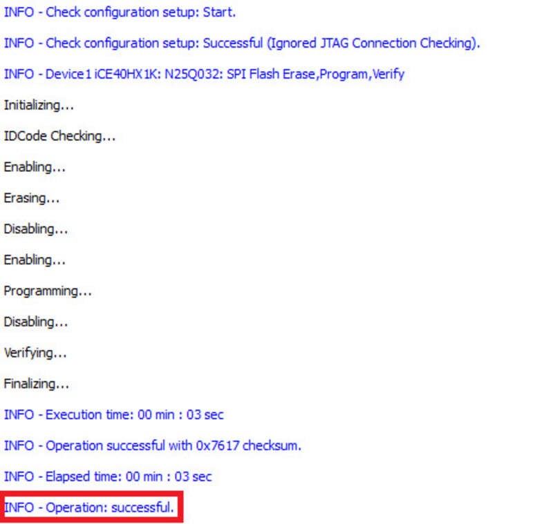
Then press program:

Making a new code: LED Blinking
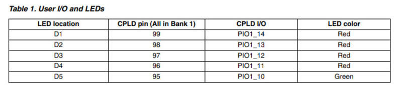
Finding the pins
To test the synthesizer, I made a quick Verilog code that made the 5 LEDs on the evaluation board blink.
LEDs
First, I had a look at which pins to use to reach the LEDs:
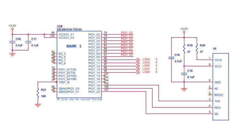
Clock
The clock (12MHz) is available on pin 21:
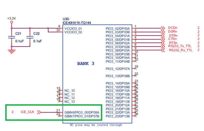
Note that a PLL module is available to provide a multiplication of this clock but I didn’t try it.
Reset
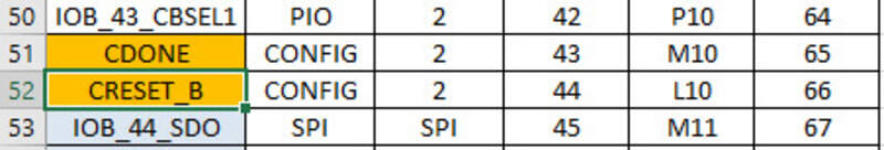
To make sure all my signals and counters are at zero at the start or whenever I (would, as I didn’t make one) press the reset button, I make sure to connect the reset signal in my processes. It is available on pin 44 and is called CReset.
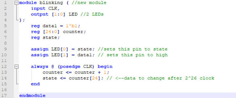
The code
The code is quite simple: I define a new module which is my LED blinker and sets its input as the clock and the output as 2 LEDs (an array of 2 bits). I then create a counter of 24bits, a data = 1 and a state that will change over time. I then assign (connect the wires) of my first LED (the green one) to the changing state and the red LED to the “high” state. Finally, every time I have a clock rising edge, I increase my counter until I reach 2^24 (67,108,864 in decimal). I always set my state to this 24th bit. That means that bases on a 12MHz clock, I obtain a 12,000,000/67,108,864 frequency ~= 0,71Hz. Almost one blink per second.
1 2 3 4 5 6 7 8 9 10 11 12 13 14 15 16 17 | |
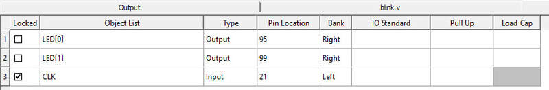
The only thing left to do is first: synthesize this code and then, during the placement and routing, set the CLK and LED inputs and outputs as actual IO pins. This can be done in the ICECube2 pin constraints editor. I found out earlier that the clock is pin 21 and the LEDs are 95->99.
Then the output code (localized by default in the project folder: \LEDBlink_Implmnt\sbt\outputs\bitmap\LEDBlink.bin) can be read in the Diamond Programmer just like before:
Result:
Last code: PRBS sequence generator
I then decided to try to implement a Pseudo-random binary _sequence. A PRBS (pseudo random binary sequence) is a deterministic binary sequence that despite being generated by a deterministic algorithm, is difficult to predict and exhibits a behavior that is similar to a random sequence.
They are therefore particularly useful to test the communication between multiple devices as you can test the communication by checking the received bits with this deterministic pattern (no need to store the values in advance) while the sequence looks like random (almost perfectly random in term of duty cycle and the zero ratio is close to even)).
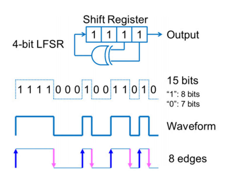
They can be physically implemented using a linear feed switch register (LFSR) which need a shift register and a few XOR gates.
I created two new modules: A proper clock divider and the actual PRBS sequence.
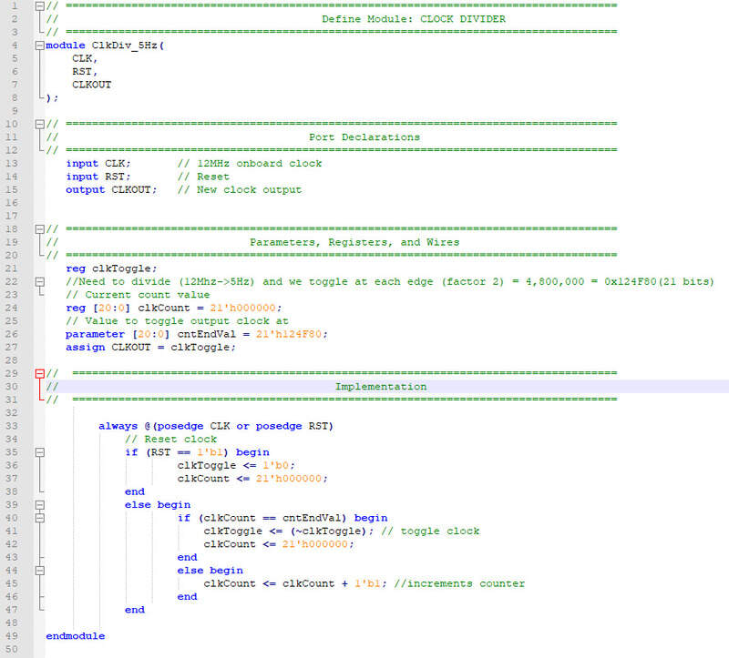
1. Clock divider
That one is pretty straightforward but has some improvements compared to my basic code: I set one input as the original clock (12MHz) but I also have one reset signal. I then calculated that to get a 5Hz clock from a 12MHz one, I can toggle my own “created” clock whenever a counter reaches a certain value. Since I toggle (only high OR low, not high then low) each time I reach this counter, I already divide by 2. To go then from 6MHz to 5Hz I still need to divide by 1,200,000 or 0x124F80 in hexadecimal (21 bits).
In the process I then toggle whenever my counter reaches that value.
1 2 3 4 5 6 7 8 9 10 11 12 13 14 15 16 17 18 19 20 21 22 23 24 25 26 27 28 29 30 31 32 33 34 35 36 37 38 39 40 41 42 43 44 45 46 47 48 49 | |
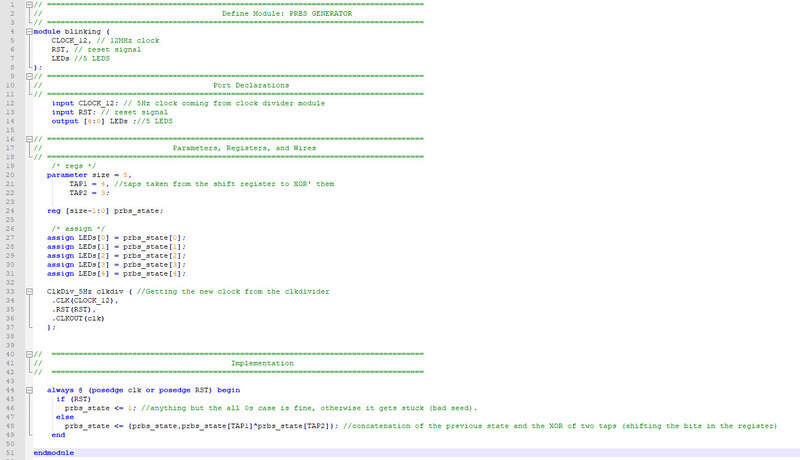
2. PRBS generator
Here the particularity is that I connect my clock divider module to my “main” module by instantiating one clock divider in my main and connecting its port to signals in my main.
I then simply concatenate (so I shift) my register of 5 bits with the XOR of the last two bits (exactly how a PRBS generator works). With this, I generate a 2^5 = 32 different bits that look random but are deterministic. I then light up my 5 diodes based on the 5 bits state of my shift register.
1 2 3 4 5 6 7 8 9 10 11 12 13 14 15 16 17 18 19 20 21 22 23 24 25 26 27 28 29 30 31 32 33 34 35 36 37 38 39 40 41 42 43 44 45 46 47 48 49 50 51 | |
3. Synthetizing and programming
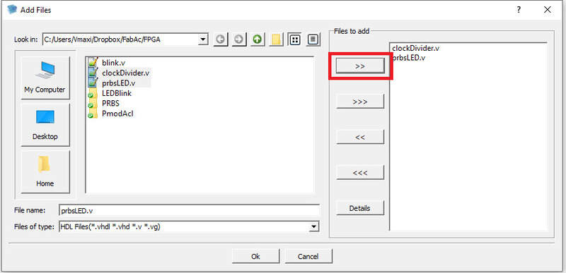
Since I split my code in two modules, I need to add them both in my design. Small tip: don’t forget to place your files on the right-hand side before clicking OK (yeah, I lost 10 minutes to this…)
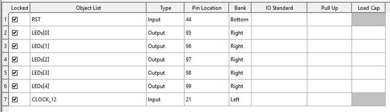
Pin constraints for the “main”
It looks random, but it isn’t !
ESP32 development board
Features
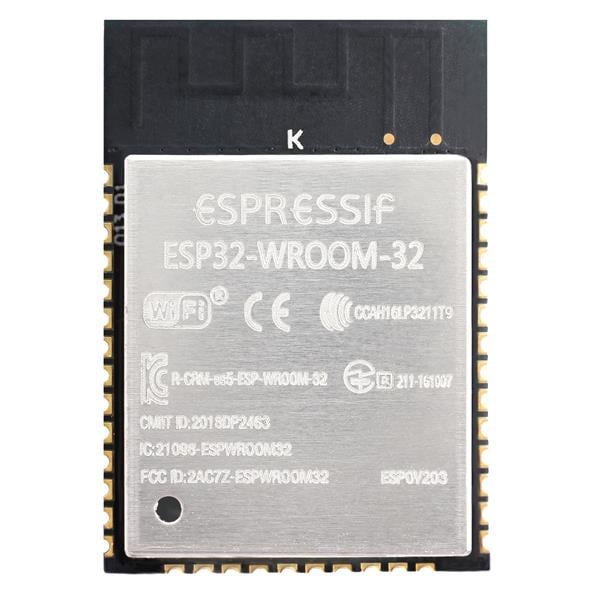
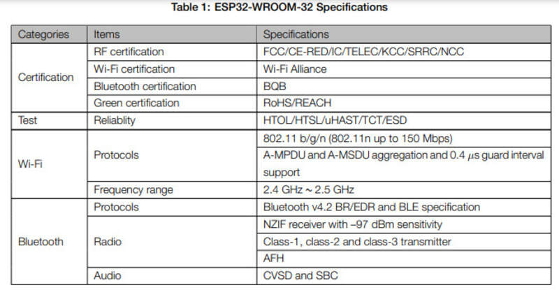
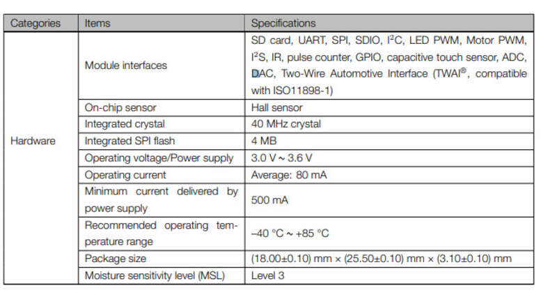
This week I also wanted to make an ESP32 development board that will probably be useful in the coming weeks. At the Fablab we have a few ESP32-WROOM-32 microcontrollers lying around so I took one with me and started reading the datasheet:
The ESP is a 32-bit microcontroller developped by Espressif that has some nice features such as WiFi, Bluetooth (normal and low energy: BLE), an antenna, hardware acceleration for cryptography applications, … as specified in its block diagram found in its datasheets(for the ESP32 family) or specifically for the WROOM32:
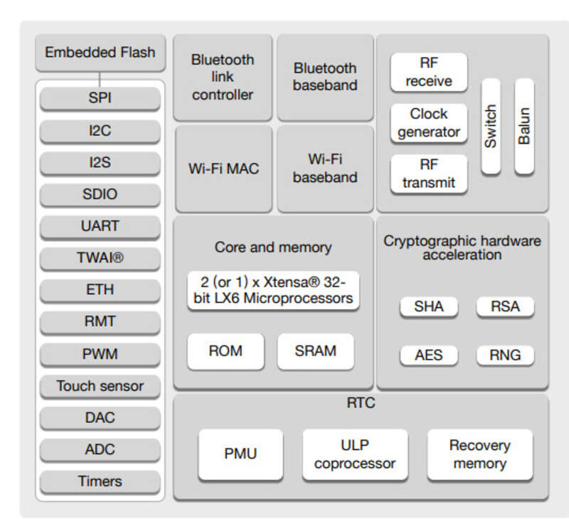
A more detailed analysis reveals that it features two CPU cores that can be individually controlled and a clock from 80 to 240MHz. There is also a low-power microprocessor that can be used to save power. Regarding its connectivity : multiple GPIOs (general purpose input and output), capacitive touch sensors, hall sensors, an SD CARD and ethernet interface and support for SPI, UART, I²S and I²C.
Additional information:
- Because of its low-power CPU and its sleeping modes (where the current is < 5µA), it is also suitable for battery operation.
- The OS for the WROOM 32 is freeRTOS.
- The ESP can be powered by a 3.3V supply voltage maximum.
Pins
GPIOs
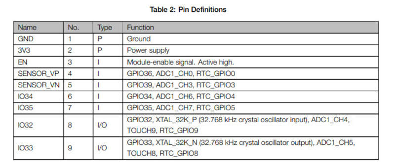
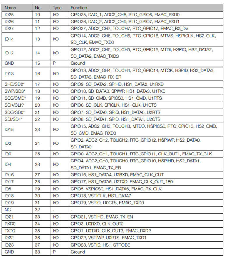
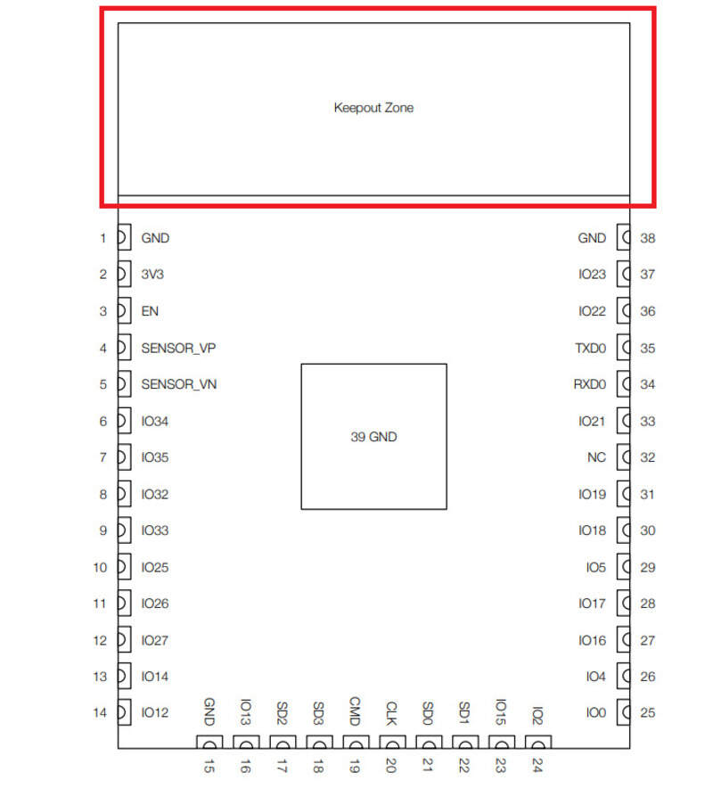
As stated before, the ESP features multiple GPIOs whose pin layout is found in the datasheet:
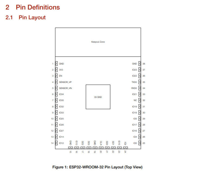
Each pin (38 in total) can be used as a “simple” input/output pin but some of them have extra functions:
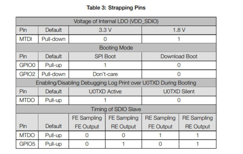
Strapping Pins
Strapping pins are pins that are used to set the ESP into bootloader or flashing mode, set the operating voltage of some other pins, … These pins should be left floating during startup as they are (weakly) pulled down or up internally except if you want to specifically change some parameters
Making a PCB
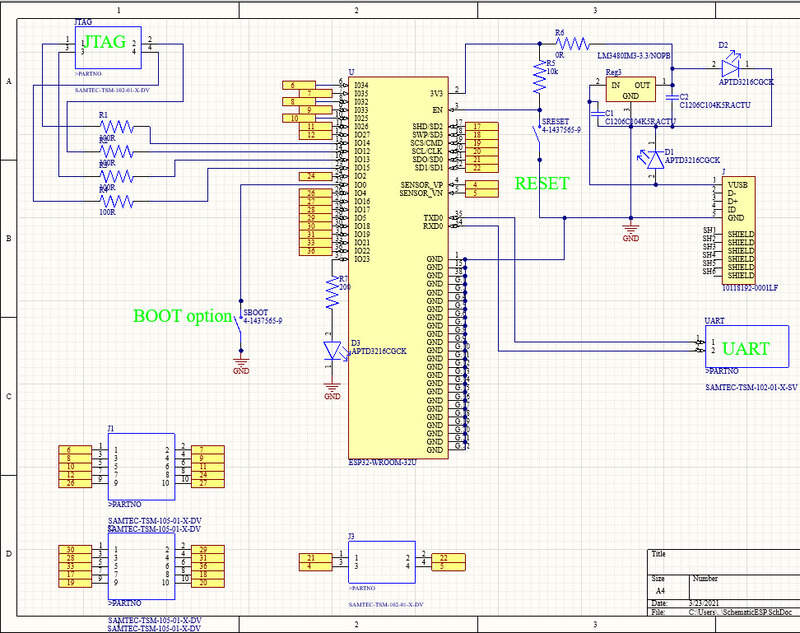
1. Schematic
I want to make a development board which means I must be able to program my ESP and have access to all the pins on the board. I also want to be able to power it via USB which means I’ll need a 3.3V regulator. Two diodes will tell me if 5V and 3.3V are coming through. Finally, a diode will be connected to a specific pin so that I can control it. A push button be able to control the booting option and another push button will be the reset. The pins will be split in multiple parts: - UART connector - JTAG connector - 24 GPIos (2x10 + 1x4)
All in all I made this schematic in Altium:
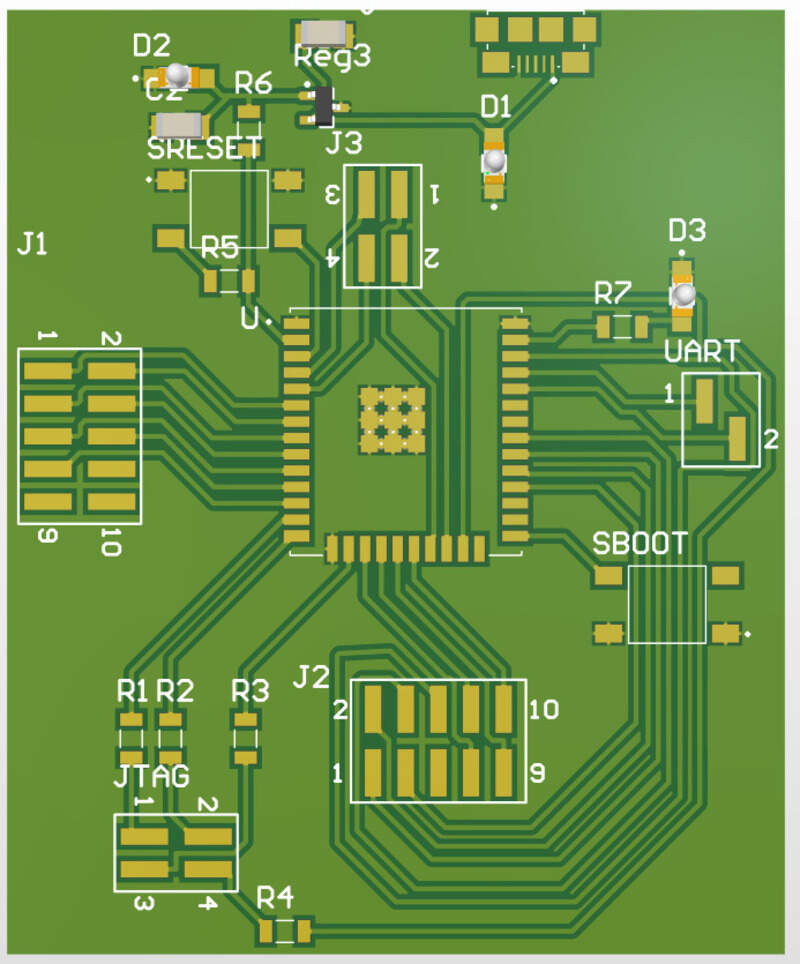
2. PCB Layout
Then did the routing and included a ground plane :
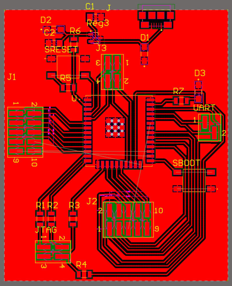
Because I’m limited to a single layer, I had trouble connecting all the pins. I’m missing three in total. Not an extremely big deal for a first version so I’ll only connect them using jumper wires. It probably could be solved by changing the pin layout but it would take me too much time (spiral/time management !).
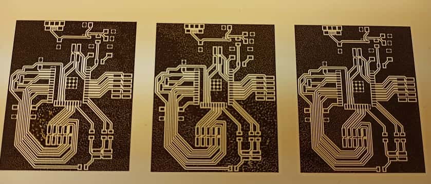
3. Production
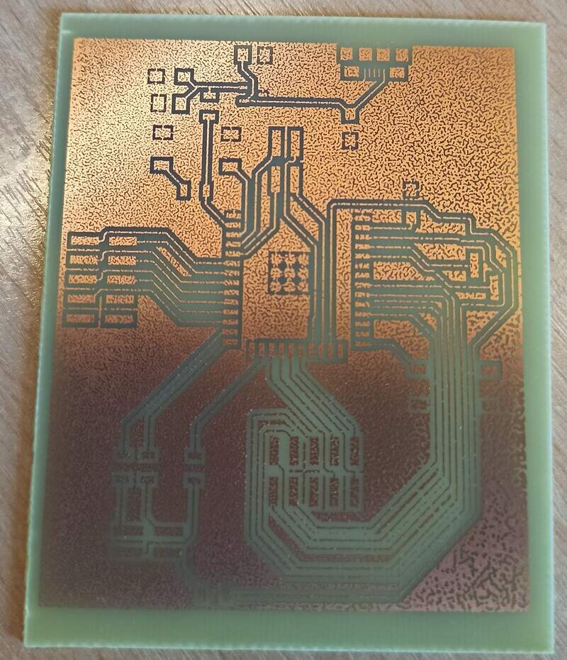
Here it becomes… Complicated. We had no more FR1 copper plates at the Fablab when I wanted to make my board… So I tried to make one by chemical etching:


I didn’t notice at first but the printer I used to make the mask was actually low on ink…

That made the board way more porous than it should be as the ink layer was a bit too thin.
So, just like I did in week 4, I tried to cover the board with tin to cover the holes but it didn’t cover anything… So I tried to apply a lot of flux and solder to cover the tracks:
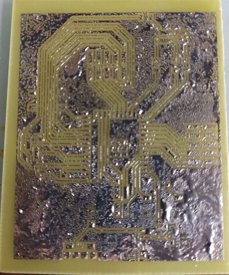
Unfortunately, it didn’t work out very well and it created a too thick layer so I cannot correctly solder my microcontroller…
All in all, I couldn’t make my board this week so I’ll have to postpone it.
Update Week 10:
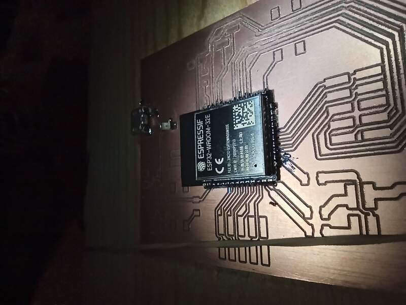
I had some time this week to finally mill my board as new FR1 boards arrived.
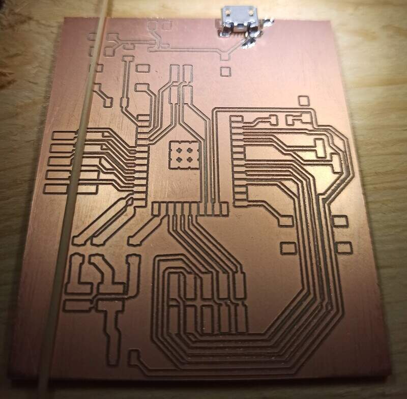
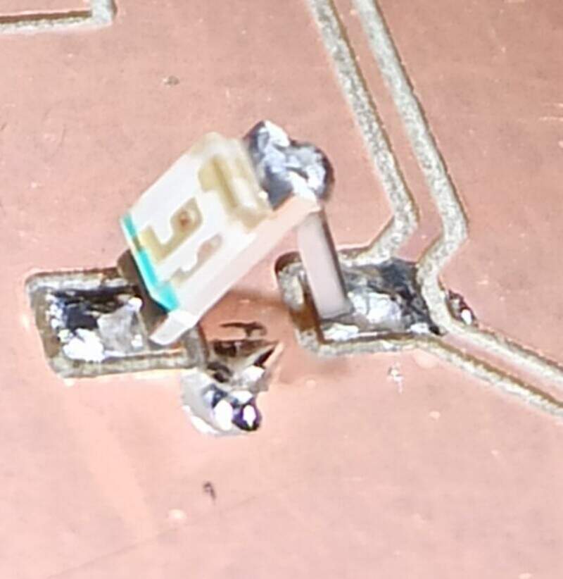
I could finally also solder it and make it work! Some issues though that should be fixed before reusing my design: The main one being that I forgot adding two current limiting resistors on two LEDs (D1 and D2). Luckily I noticed it during soldering so I could repair that mistake.
Also, during production, I once again had the issue that ground pads are completely isolated like other pads instead of being connected to the ground plane… I though I fixed that issue in electronics design week but it seems that Bantam Tools CNC machine didn’t remember the settings or something else gone wrong. Again, easy fix to add small pieces of wire to correct that.
More ground pins would be useful to add here and there, especially near the UART connector.
The ESP32 has a “keep-out zone” (I think due to the antenna) which was not indicated on the footprint I took online so two pads are not accessible anymore.
Finally, a strong pull-up would be needed on GPIO0 to make sure we boot in SPI mode and not in download mode by default (it works sometimes but a strong pull-up would help make it more reliable). Otherwise, you sometimes need to short 3.3V and the GPIO0 to be able to enter the SPI mode.
Soldering the ESP32 is not an easy task by itself as the package is almost like a QFN, meaning you have to “push” the solder underneath the pads to make a good connection. Anyway, with a bit of practice, it’s a matter of minutes.
All in all, the ESP32 can be programmed easily and works well. I used it for the input devices week.
My design files
My ESP32 Altium design and my FPGA codes and bitstreams are available here: My Design files