Week 6
Electronics design
Assignment
Group
• use the test equipment in your lab to observe the operation of a microcontroller circuit board.
Individual• redraw the echo hello-world board, add (at least) a button and LED (with current-limiting resistor)check the design rules, make it, and test it
• extra credit: simulate its operation extra credit: render it
Group Assignment
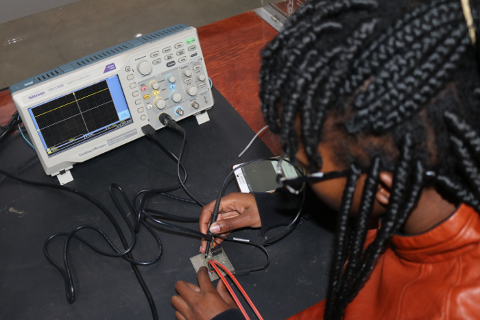
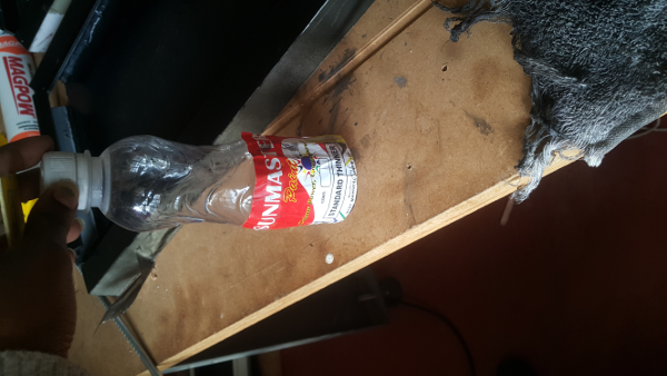
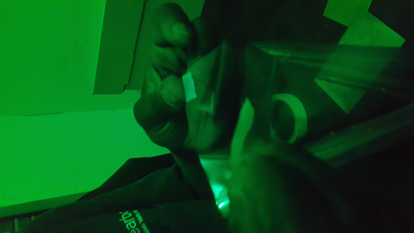
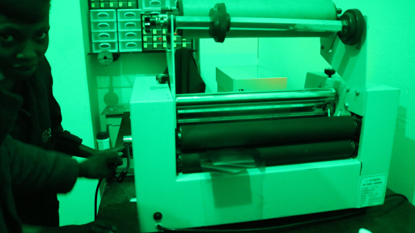
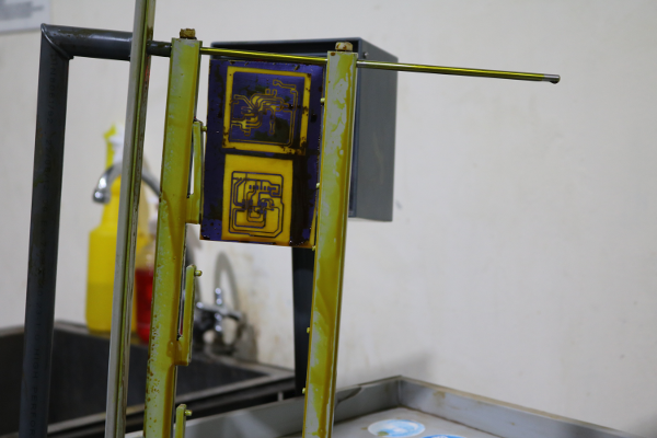
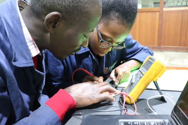
For this assignment I used an oscilloscope which in an electronic test equipment that observes signals like voltage etc which we have in our labs as shown below. Performed the below tests.
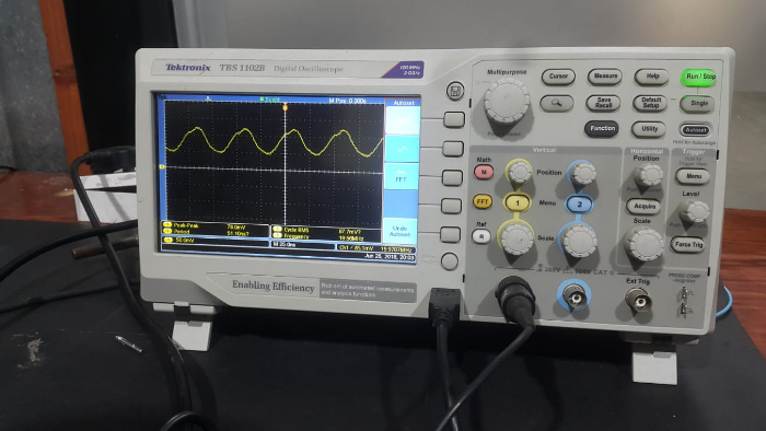
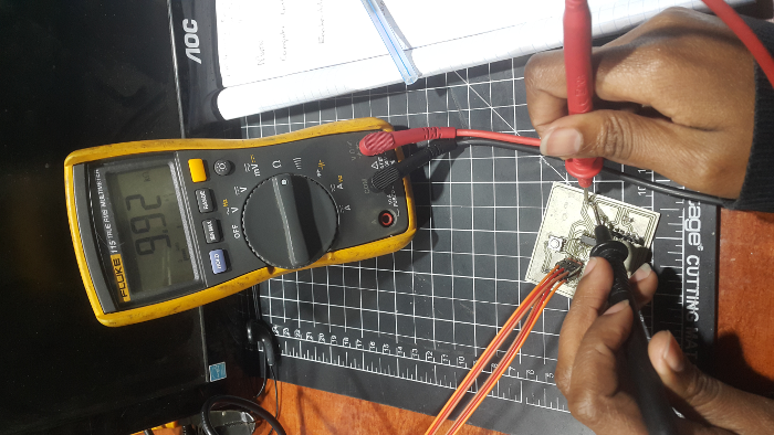
Clock frequency test using a Crystal
Started by testing out the resonator in the hello board that I designed for this assignment. I powered the oscilloscope,then from the board I connected the ftdi cable pins on oneside while on the otherside I plugged the usb into the oscilloscope. Using the plug from the oscilloscope I connected it to the board the gnd and the other pin for testing.
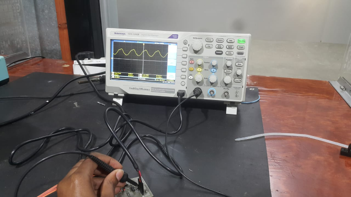
The cystal creates electical signals which provide a precise frequency that is used to keep rack of time. The oscilloscope reads the crystal clock signals as shown. The crystal that I used has a clock frequency of 20mHz which in this case the oscilloscope read the same 20mhz.
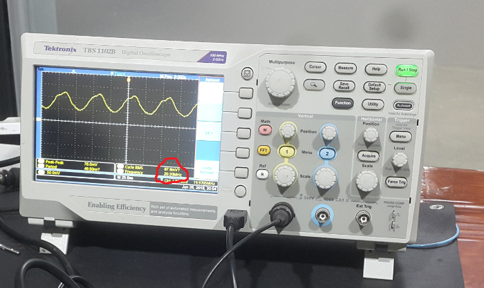
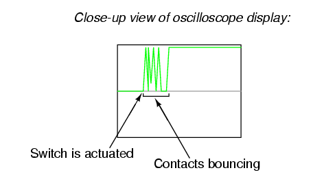
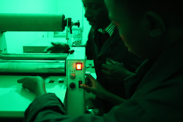
Contact Bounce Test using a button
While I was testing the button push continuity it experienced a contact bounce before it stabilized as shown. When I pressed the button it experiences an oscillating activity as shown then it stabilized as shown in the consecutively.
When a switch is actuated and contacts touch one another under the force of actuation, they are supposed to establish continuity in a single, crisp moment. Unfortunately, though, switches do not exactly achieve this goal. Due to the mass of the moving contact and any elasticity inherent in the mechanism and/or contact materials, contacts will “bounce” upon closure for a period of milliseconds before coming to a full rest and providing unbroken contact.
Reference link from:https://www.allaboutcircuits.com/textbook/digital/chpt-4/contact-bounce/
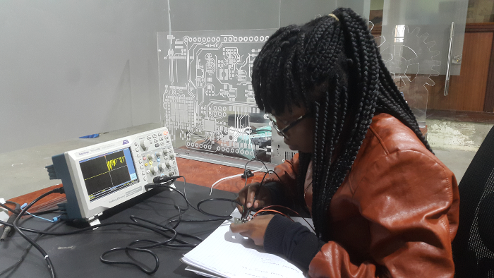
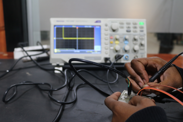
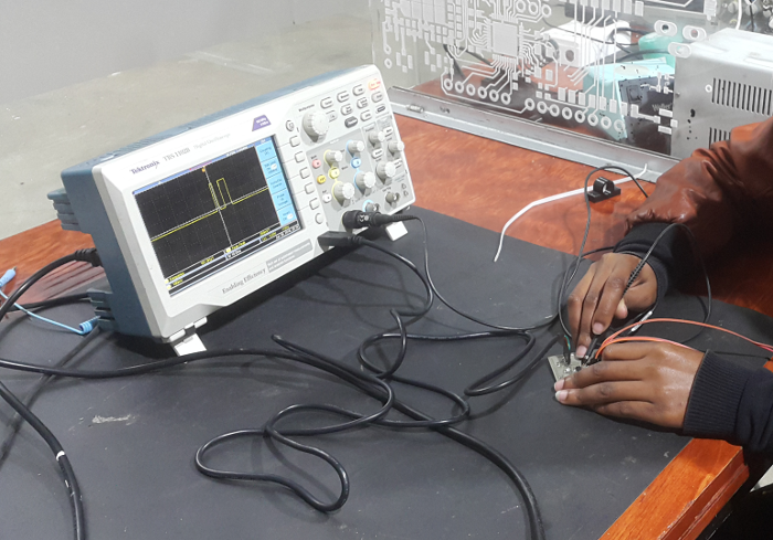
Serial communication
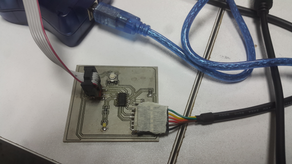
To test the serial communication of the microcontroller and the board. I had programmed the board to send a different letter when pushed so i placed the pin of the oscilloscope to the TX pin of the microcontroller(ATtiny44). The oscilloscope displayed a shwon when I pressed the button.
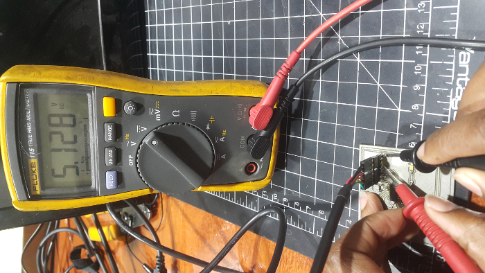
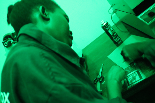
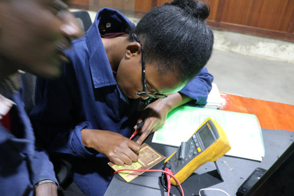
Multimeter Test
Measuring resistance
I had 3 resistors in the board which where one 499 resistor and two 10k resistors. Using a multimeter I mooved the probe to the resistor
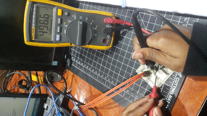
Measuring Voltage
To measure the power rate for the ftdi cable that was being used to power the board I connnected the GND with the VCC. The multimeter displayed the voltage as shown.
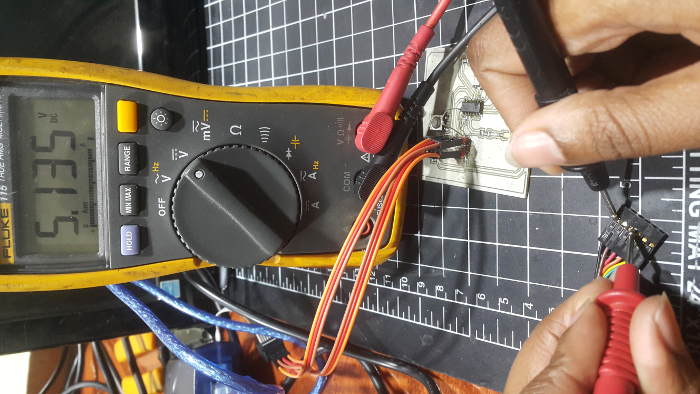
Shwoing the similar voltage when connected to the board
Individual Assignment
Hello World board
Am new with electronics software and electronics in general so i had to got through some tutorials. In this case I used Eagle software to design the board. I just downloaded it online and installed it.
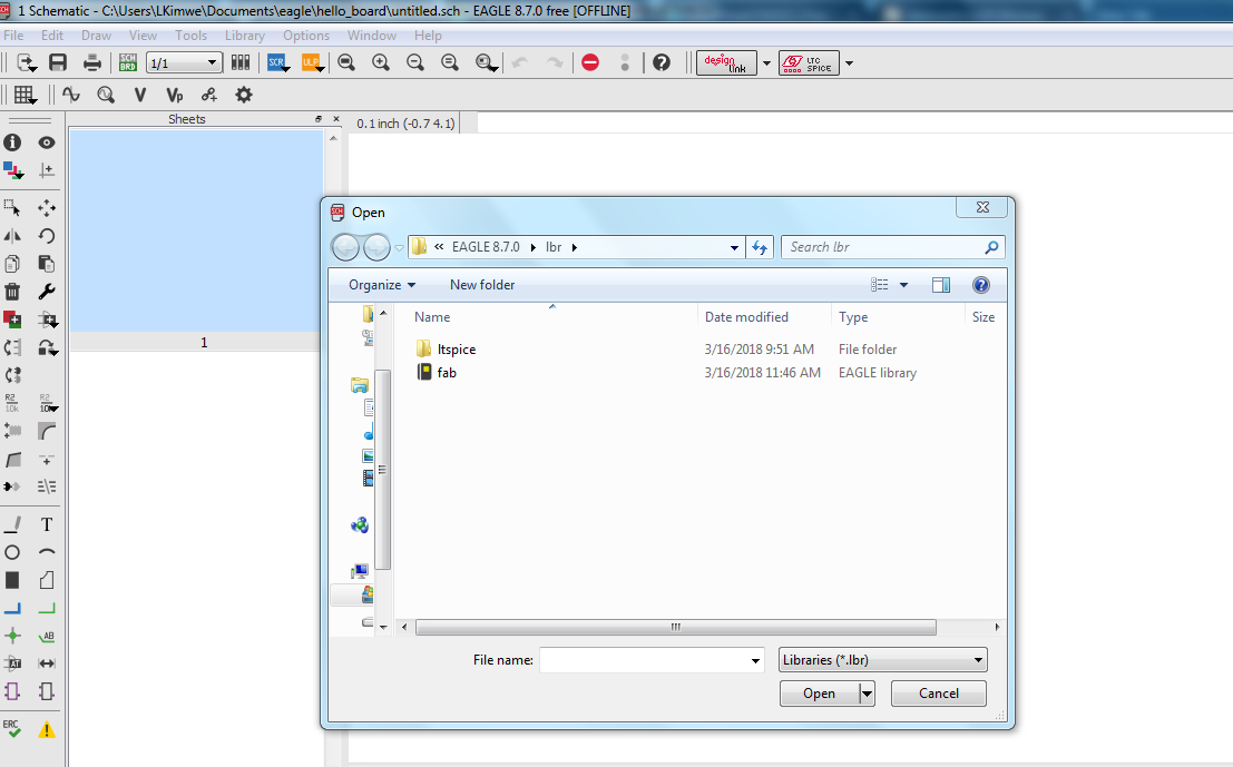
Downloaded the fab library then imported it to eagle. at first i started a new project then when to library then open library.
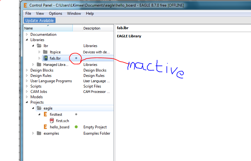
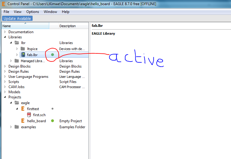
I came across afew challenges specially with importing the fab library and for you to be able to view I didn't know you have to activate it. later i figured that out.
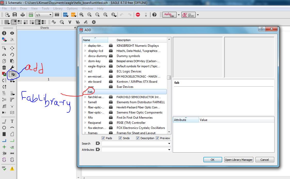
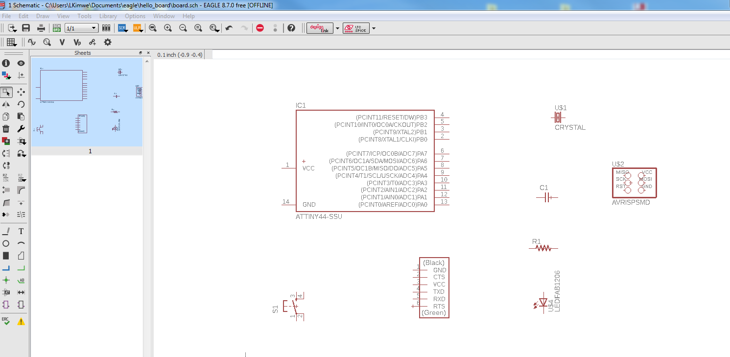
At first i had to learn what the components looks like in there symbol forms, some of them i knew already and others i had to familiarize myself with.After creating a new project. opened a schematic where i dragged components for the board. using the add button that shows a list of components and libraries.
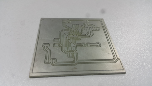
My schematic with all the components.
Finaly i got the flow of the components and how to connect them. My schematic with the connections and labels shown.
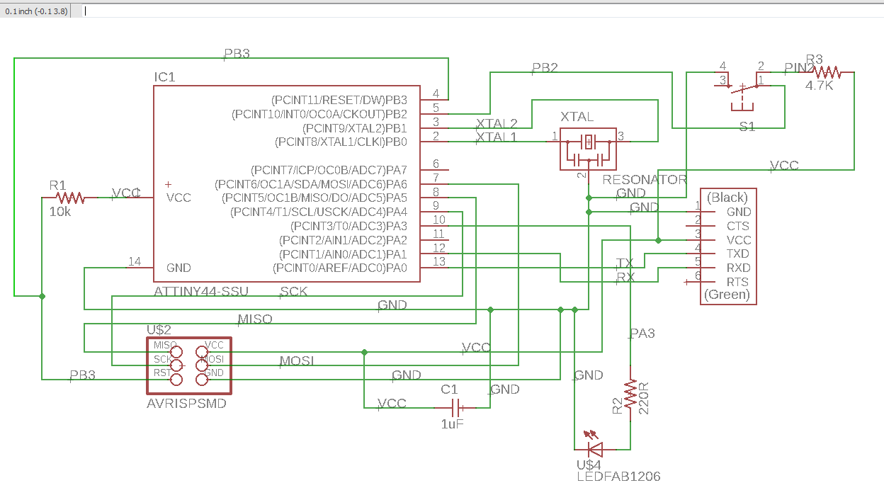
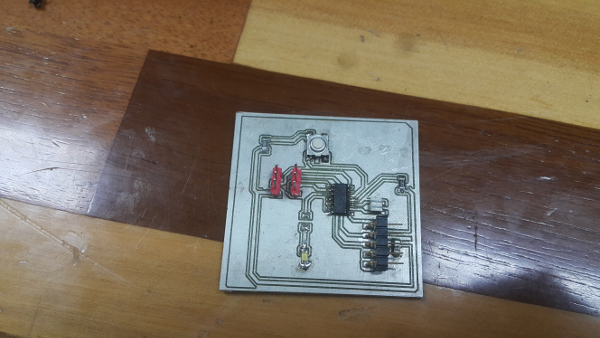
In the final board with the LED and the button included in the design.
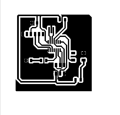
This was the first board i had made so i just printed as it.
Challenges
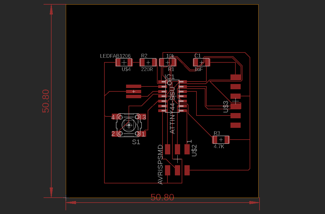
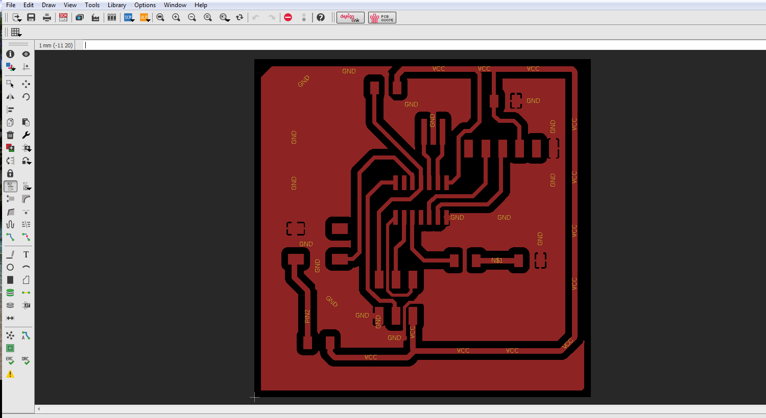
The challenge that i had was the routing of the board where some lines where really close to each other until they where touching the components so i as shown below. Many components where atttaching to the GND.
Solution
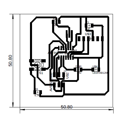
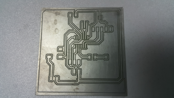
This time round i changed several things from the design. Since i had several components connecting to the GND i decide to put the surface of the board as the ground.I firt used the polygon toll to round the whole design. Gave it the GND name and it grounded all th ecomponents. clicked the ratsnest tool to view.
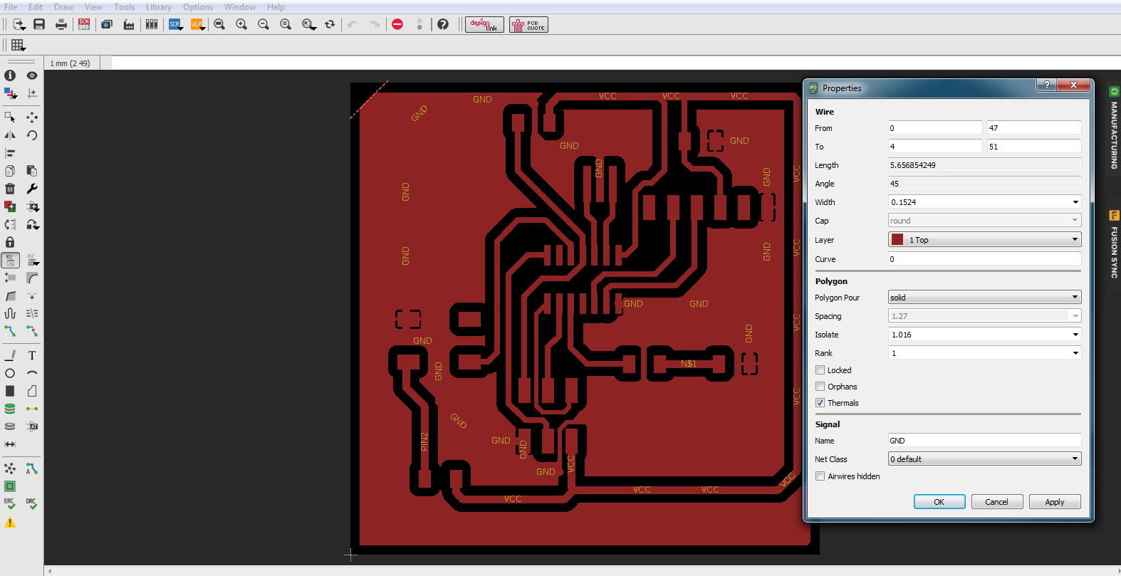
Then right clicked on the polydon to view properties. In properties view i defined the isolation distance between the lines.
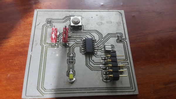
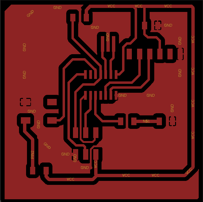
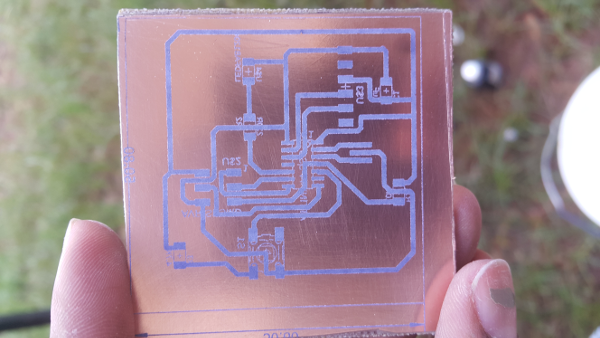
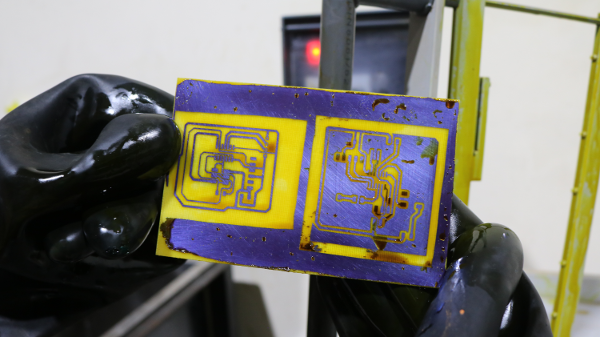
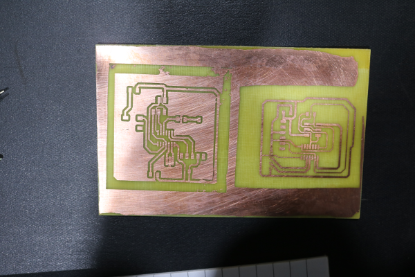
The final board for the hello world .
1st Etching process
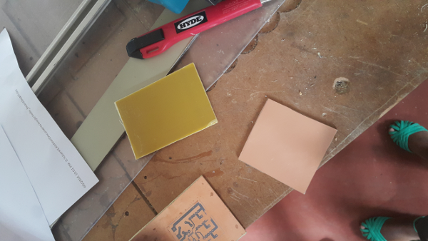
For the etching process i used a single sided board since it was a long strip and my board had specific measurements i cut it into upto the measurements that i required. i marked the position to cut first
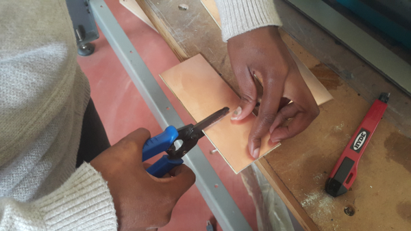
I found it is easier to cut using a knife so i run the knife from th emarked point to the other end making sure the line was staright i used another board as shown.
Then cut it into half and since the edges became a bit rough and not straight i just straightened it using the small knife like shapening it. surprisingly the board wasn't that hard.
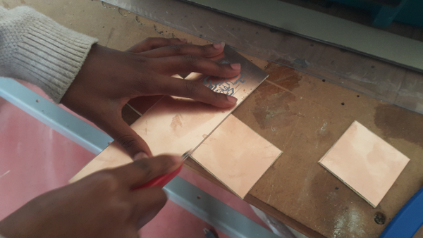
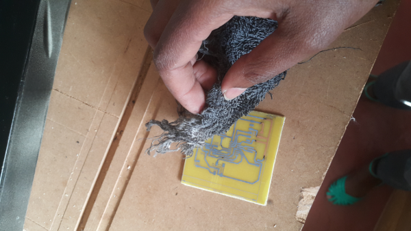
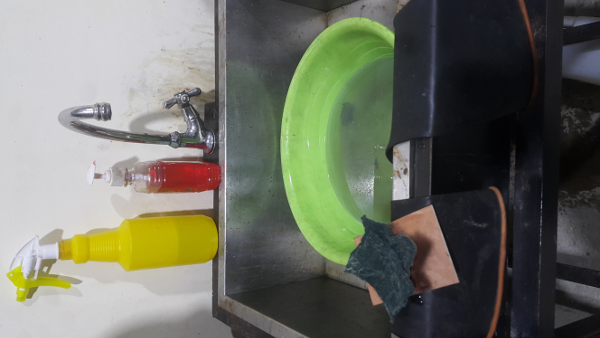
Cleaned the board using a dry steelwire to remove dirt.
Already cleaned board.
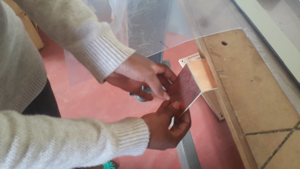
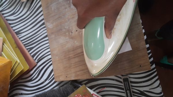
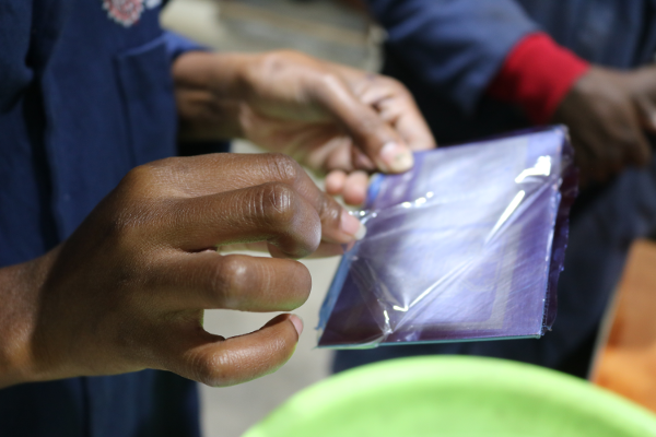
I used the image that i had printed for the board.
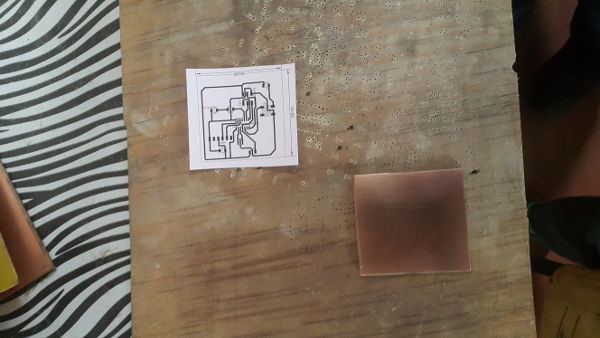
I put it carefully on the cleaned board as shown.
I used an falttening iron box to press the two together so that the paint can rest in the board. Pressed several times making sure i dont burn the paper.
After i had preesed it for sometimes i let it cool down then i removed the paper. Unfortunately it hadn't sticked on properly i was told i didnt sspread the heat well so this is how it came out.
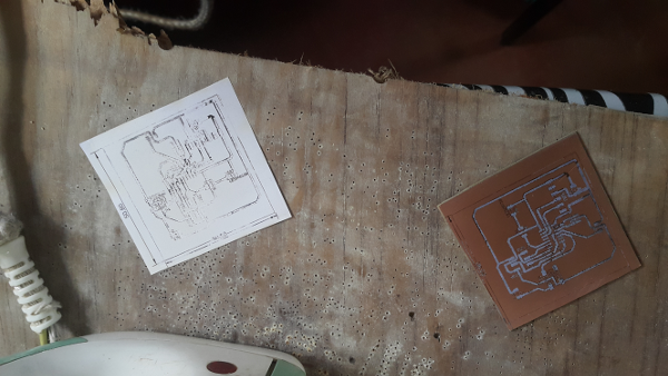
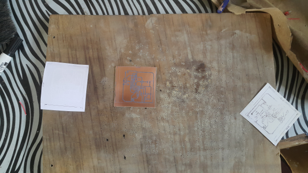
I had printed several borsds so i redid it and this time aroud it came out nicely.
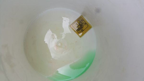
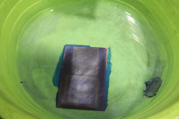
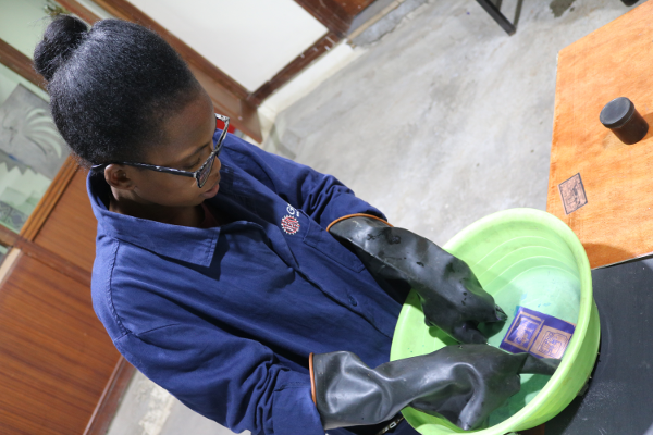
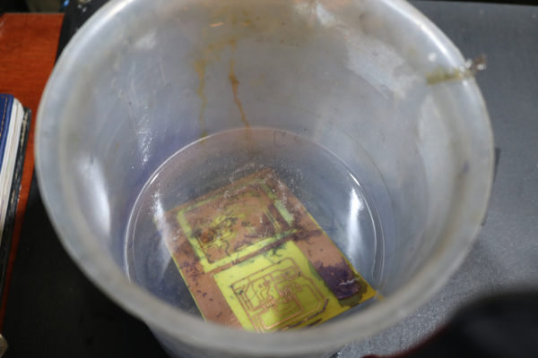
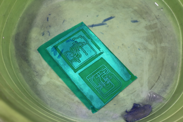
The board is sopped to be dipped in a solution to remove the unnecessary compper form the board. the solution was a mixture of HCl and hydrogen Peroxide in eqqual portion.
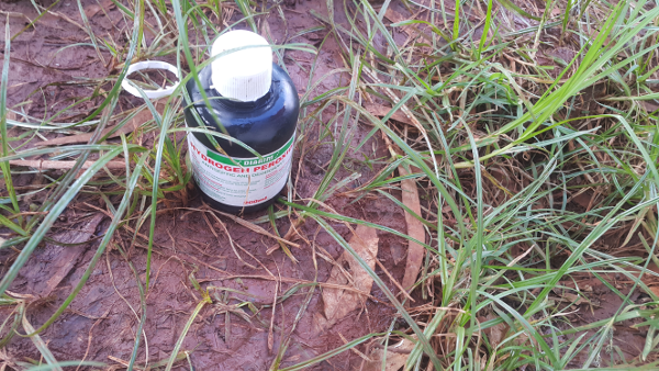
We used a bucket to put the ingredients. I had the help of a collegue in the lab who was also explaining the process and helping me understand what goes on.
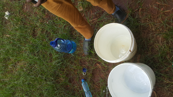
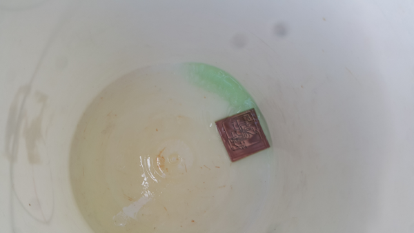
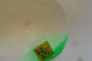
Dipped the board in the solution and in afew seconds you could see the board started changing and even the color of the solution.
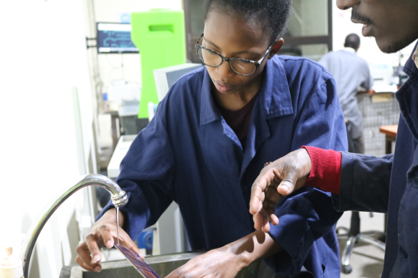
Then rised the board with water.
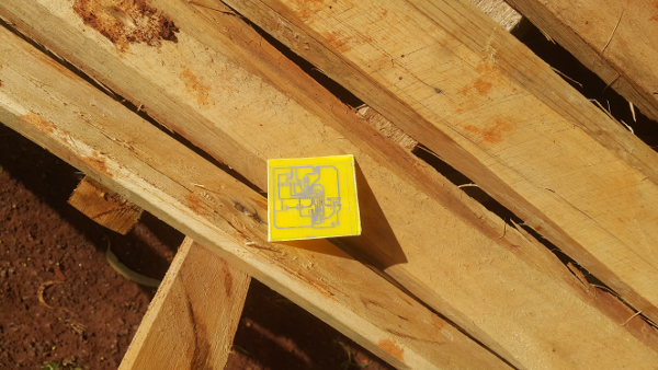
Then dried it in on a bench where there was sun. It took few minutes to dry.
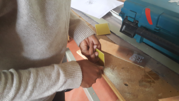
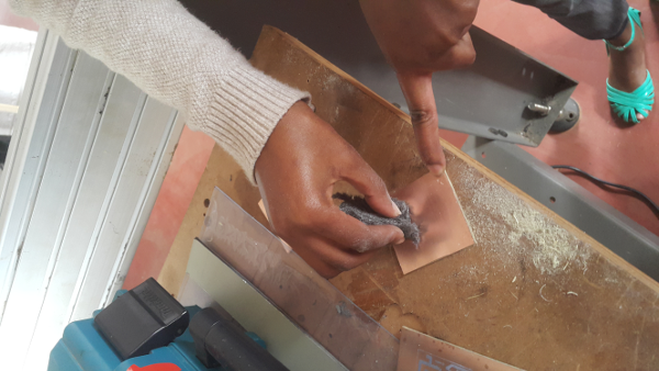
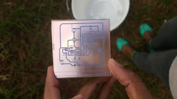
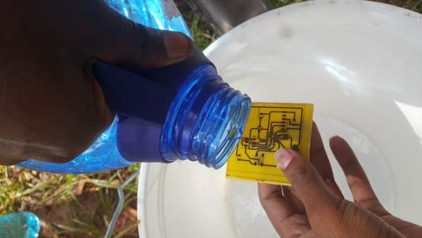
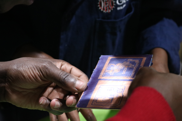
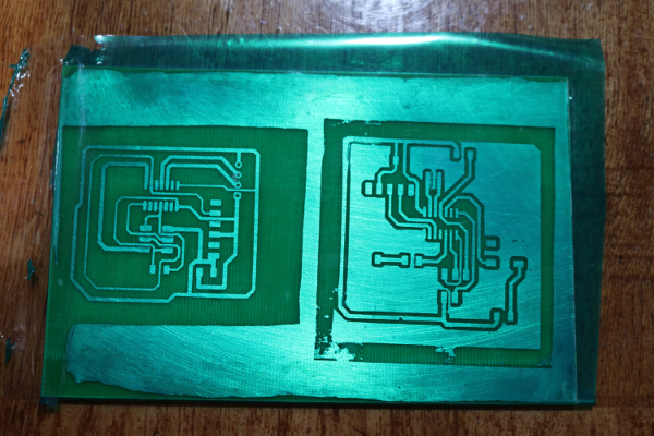
Used the thinner to clean the board to expose the copper coat and a wiping material that i soacked with the thinner.
Once i was done i was told i needed to remove the silk from the board in the software design before printing it.
2nd Etching process
The first step was cleaning the etching board with a scouring pad and washing agent.
After cleaning it I dried it by pressing it through a drying sponge .
Then i Used a drier to completely remove the excess water.
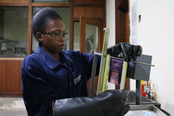
The next stage followed was a photoresist process where i laminated the board with a photoresist film. Worked with one of our lab engineers here at Gearbox.
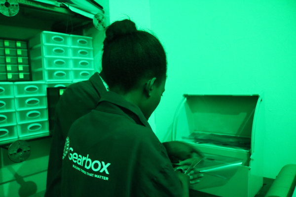
I was told that the film has three layers so we used the maskingtape to remove one of the film. The photoresist is in themiddle so we had to remove the top film and the remaining sticky part i put it on the board.
Then i used the lamination machine to press the photoresist material to the board. We used 75 degrees celcius to laminate the board. The machine has two sides so at first I pressde it then laminated.
Then I put the board design that i had printed on the board
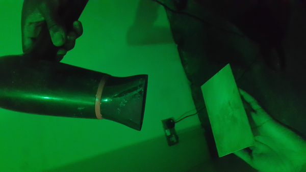
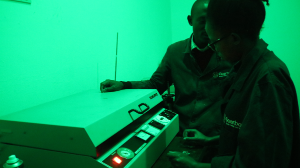
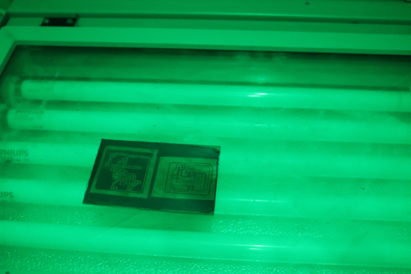
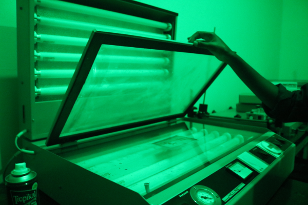
The next step was exposure using the bungard exposure unit. The unit has an inner layer called the vacuum that sucks the air out of the board once you place the board. Then press the ventilator button basicalluy want it does is to remove th eair around the board.
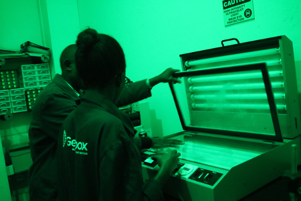
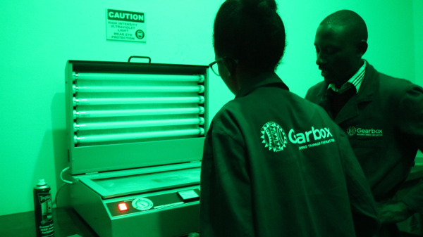
Then exposed the board into the UV light rays for 6 seconds.
Developing stage
Fistly i removed onother layer of the film. Then did a mixture of 100ml of water to 2g of sodium carbonate. In this case i used 500ml of water to 5g of sodium carbonate.Then dipped it in th esolution for sevreal minutes.
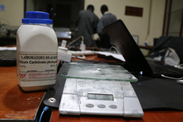
Rised it using running water then dried it.
Challenge
The major challenge was after dipping the board in the solution it still has some parts of the photo resist that had not come out properly so after rinsing i put it back in the bungard exposure unit and exposed it for a few seconds and the put it back to the solution and used my fingers to clean the excess material.as shown below in sequentially.
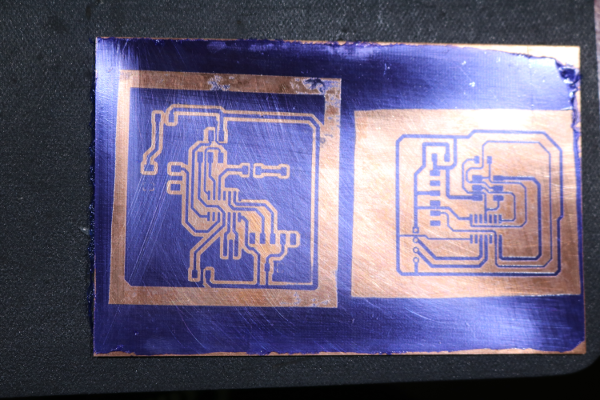
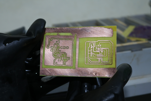
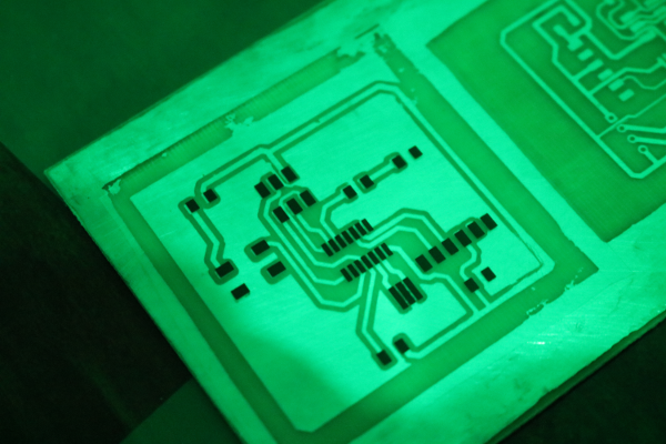
The chemical etching process
For this process I used the Bungard spalsh center machine in the lab.In splash section I used the foric chloride solution. At first had to put th eboard in place befor dipping it in the solution. The machine has a timer which you set, i set it to 5minutes.Removedi tthen rised it.
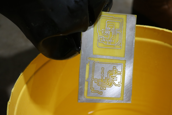
The stripping process i used sodium hydroxide with water then i dipped the board.
Dried the board then tested it using a multimeter the continuity of the connection between the commponents.
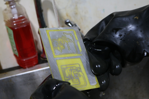
Challenges
Some of the connections had connected together at some point doo i had to manually scarp of the bits of copper attaching th econnections as shown. The results
Before
After
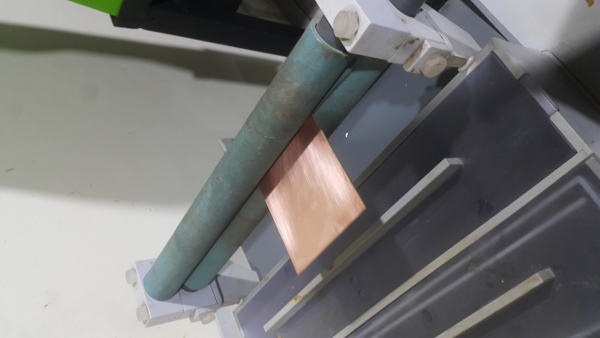
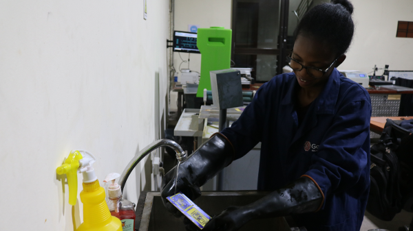
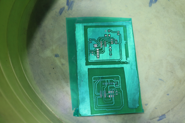
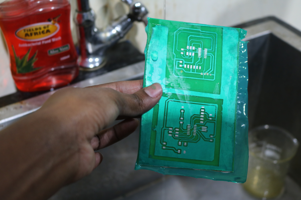
The Tinning process
Used the tinning solution to help prevent th ecopper form oxidation. I just dipped it in the solution for a few minutes then rised it out.
Soulder Masking Process
I did almost a similar process like etching. First i covered the board with soulder mask film after removing th etop layer.Then used the lamination machine to press the film on to the board.Then printed the components from the design in eagle software. Then used the bungard exposure unit to vacuum it and passed the uv light
Once done I removed the second layer and dipped it in th emixture solution of sodium carbonate and water. Rised it then dried it.
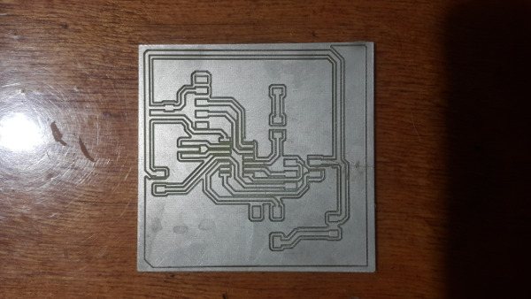
Milling
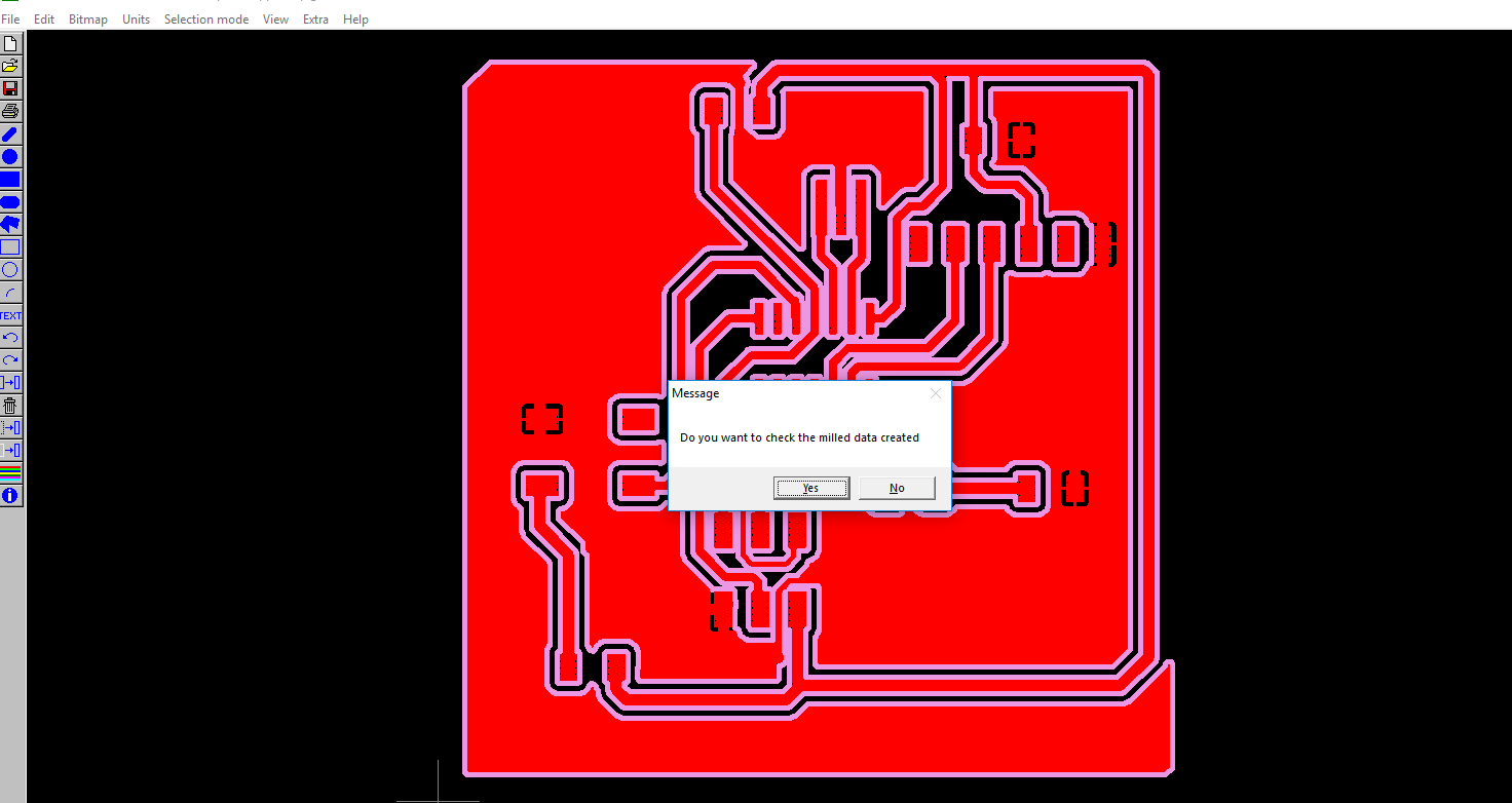
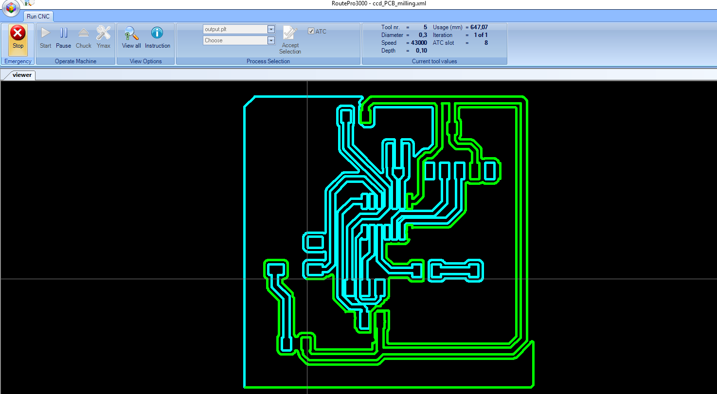
I finally found a tool to mill the boards. From Eagle software I downloaded the garber files for th eboard. then using the Isocan software I loaded the garber file as shown. A prompt pops up allowing you to specify some details like the tool to use.
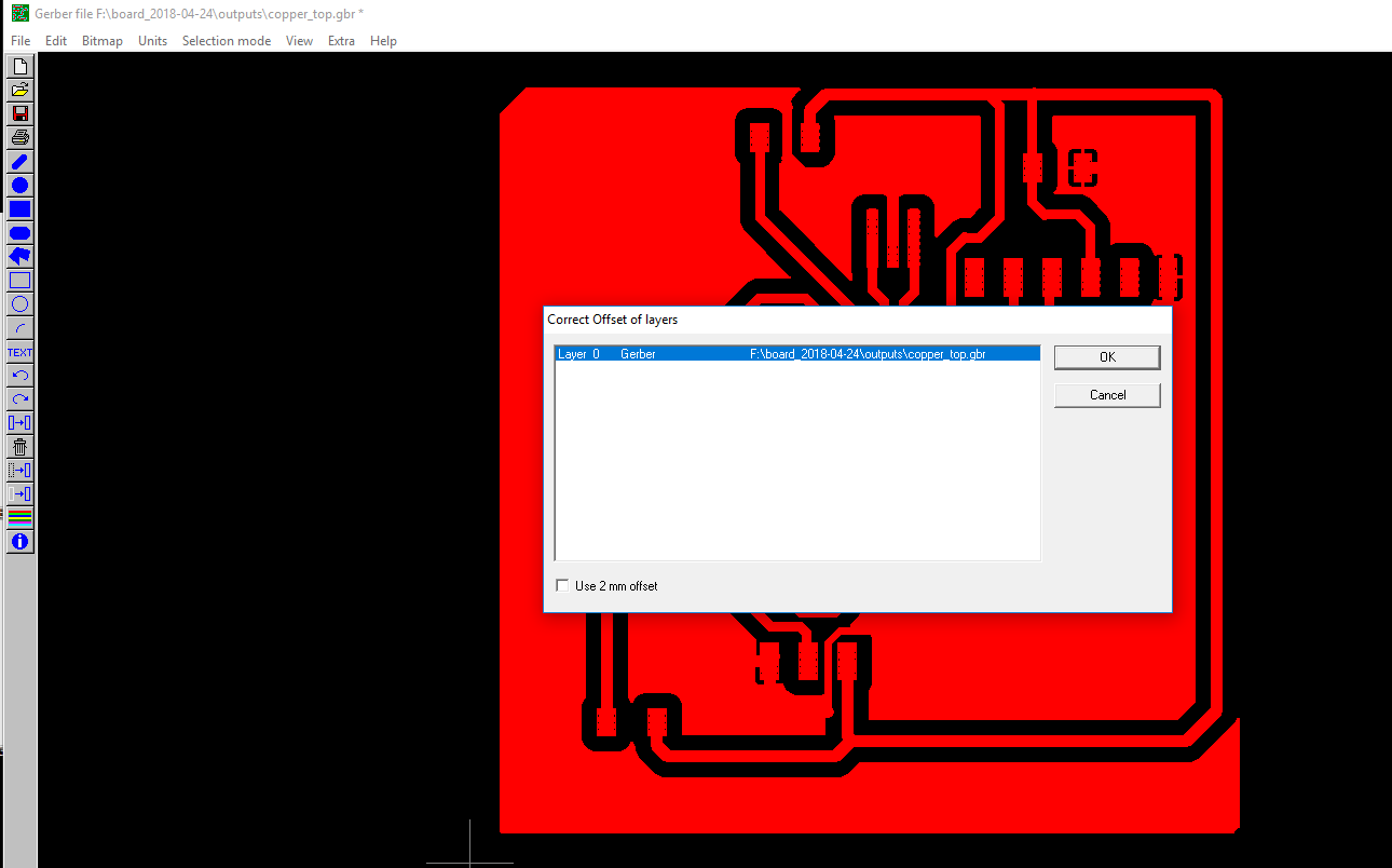
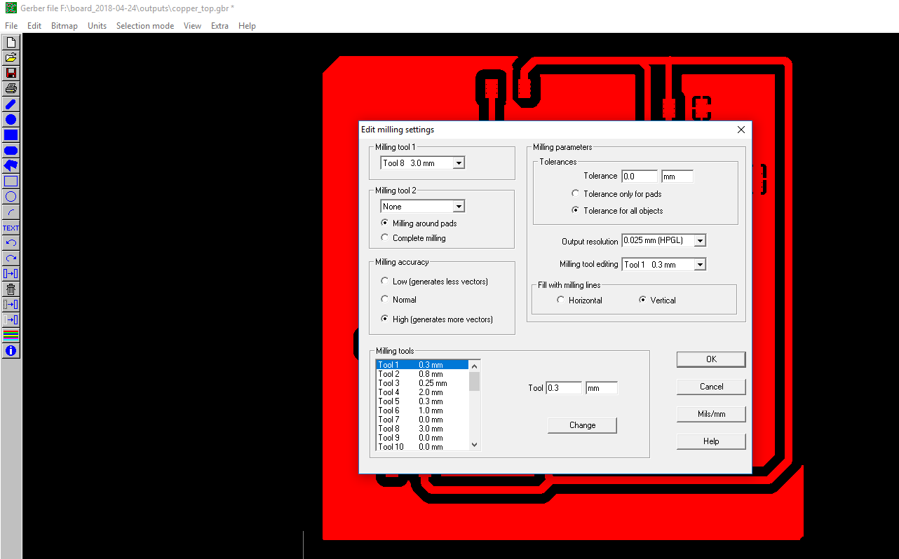
When you create the milling data from the file drop down menu it shows you the path where the tool will pass. Then you can save the milling data as a plt file.
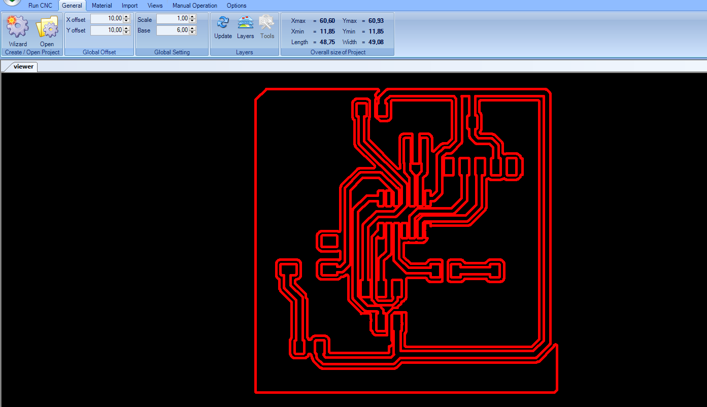
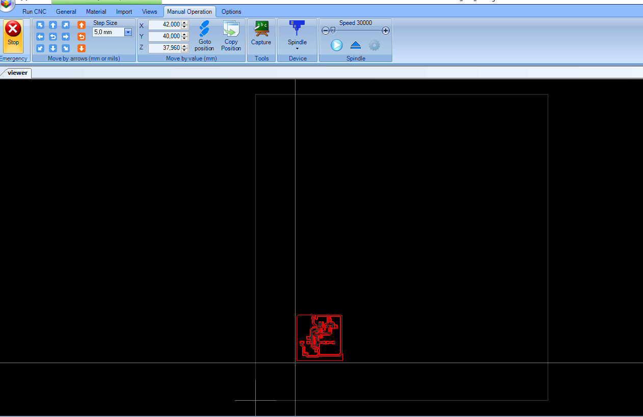
The plt file is now used to mill with the ROutepro3000 software by creating a new project then selecting the design file. Here i changed a few settings which include the x and y position of the board.
The milling information when the machine is milling.
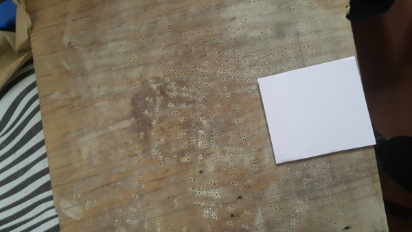
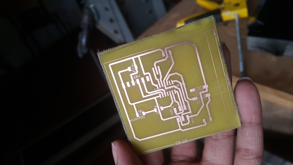
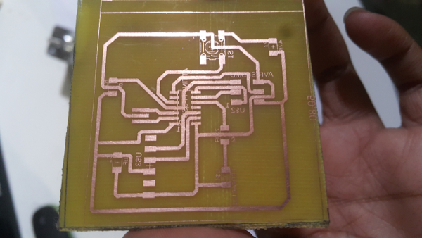
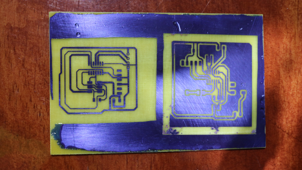
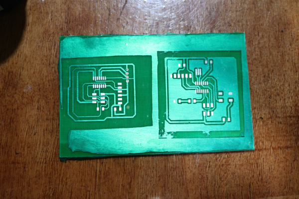
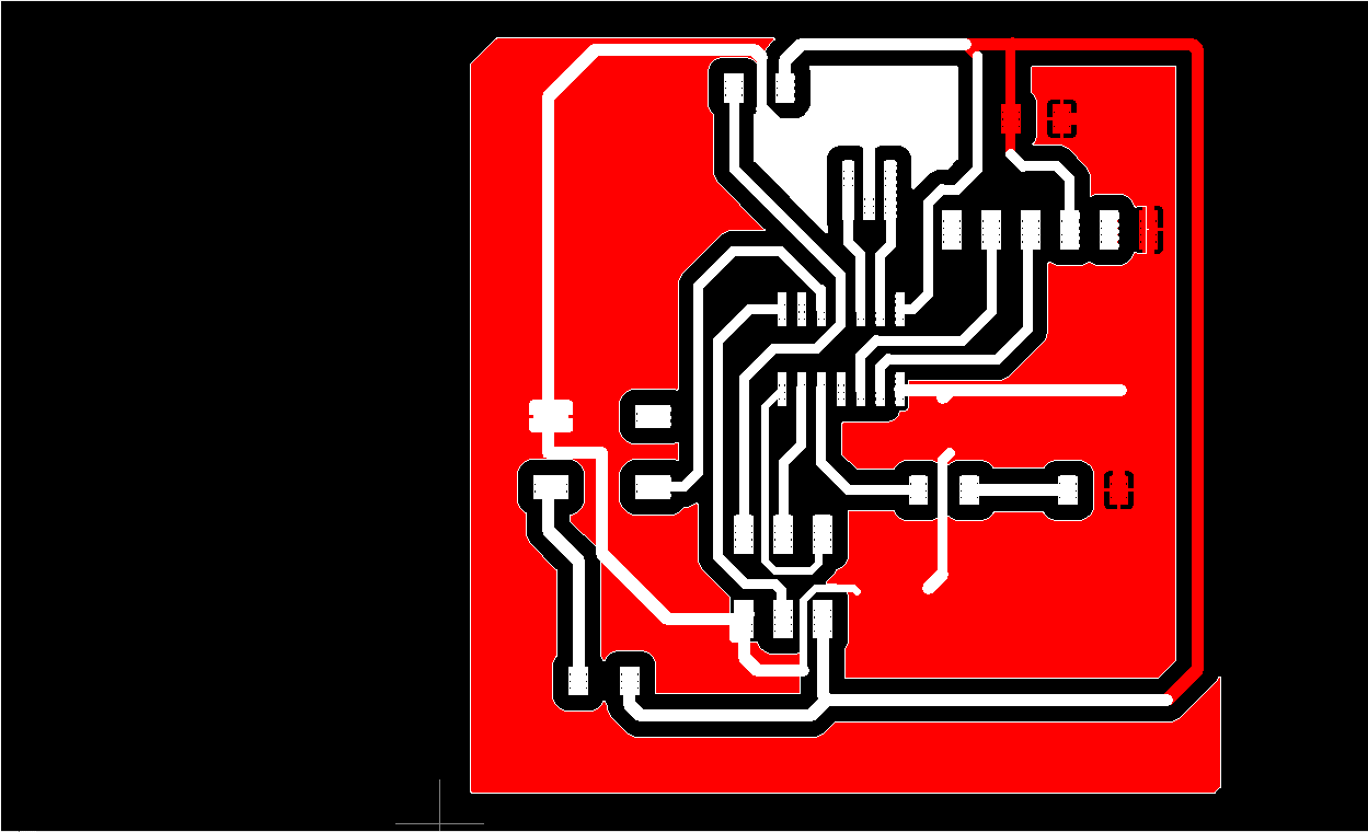
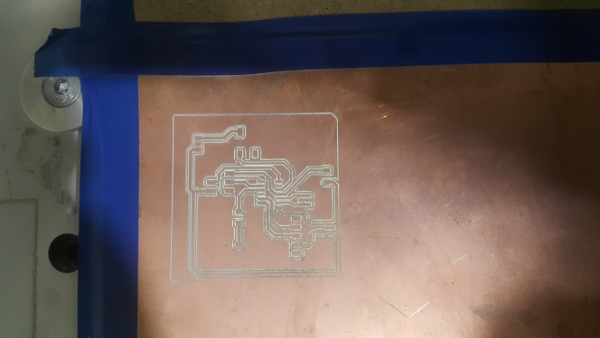
The milled board.
The final board after washing it and then dipped it in the tinning solution.
Soldering
For soldering I just used the soldering wire, flux and the soldering machine. At first I tested the continuity of the connections. The soldered and populated the board.