
1.1
For this assignment I started with downloading the original design of this ATTiny44 version of the echo hello-world board (see this page).

1.2
After having installed the Eagle software and all libraries needed, I redrew the board as per the instructions of our instructor/ guru Bas.
Assignment 2: Add (at least) a button and LED (with current-limiting resistor)
2.1
I added a button, an LED and a resistor to the schematic drawing and checked if all wiring was done correctly.

2.2
I switched to board mode for the routing of the board. It took me quite some time to figure out a proper routing. A trick that I did not use, but read about later: use a resistor with value zero to get over a line.
Assignment 3: Check the design rules

3.1
We learned what DRC is and how to use it. (It would be good to make a list with all values to use for the equipment and board material at FabLab Reykjavik.)

3.2
We also learned how to export the board once the DRC check gave zero errors. See my notes on the Bas pages.
Assignment 4: Make it

4.1
To print the board 2 files are needed: the traces and the inside. To do this some juggling with layers was needed.

4.2
In the Expert Image requester it is very important to set the resolution at 1500 dpi. Otherwise the Modela will not be able to trace the board properly. It is also important to checkmark Monochrome.
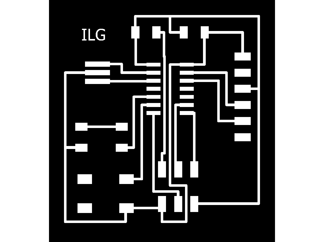
4.3
The Traces as they came out from Eagle. (Later I discovered one link is missing. I could have discovered this earlier by checking with the original board).

4.4
This was my Inside.png file (to be inverted before milling, which initially I forgot!)

4.5
While the Modela was milling I made a handwritten draft of this component list. Lesson learned: if possible, do this first! It really speeds up soldering later, especially since the resistors often are unmarked and have to be measured.
What went really wrong.

Once all components were soldered to the board I thought it really looked good. So I started programming the board, following Linda Wanders 2014 notes. BUT ....

I got an error message. After switching cables, programmers and laptops the conclusion was: faulty board. Bas immediately saw a connection was missing between IC1's pin PB3 and the R1 resistor (or RST pin of J1). How could this happen, since in the schematic drawing the connection is visible. It also is visible in the board layout as it was BEFORE I started juggling with the routes to solve DCR issues. A tiny yellow line apparantly had reappeared that I did not notice, resulting in ...

... resulting in a not so tiny physical yellow wire on my board to fix the problem! Lesson learned: really zoom in very closely on the board layout when making changes to solve DRC issues!
Other lessons learned

First I forgot to CALCULATE before pressing SEND. The Modela is then going to do the same job it did before. After following the procedure described in the 6.2 part. I wanted to continu and then found out I forgot to invert the Inside file. It might be better to make a check list, because there is so much one can forget.

To stop the milling process: press VIEW and the the UP and DOWN button together. Wait till the Modela is done viewing and restore your error.
FILES: All files of this week can be found here.
