Electronics Production
Work to be done
- Characterize the specification of yout PCB production process
- Make an In-circuit programmer by milling the PCB (program it, so I can use it).
Introduction
In this asignment I will be using design found in Brian's work on designing the FabISP.
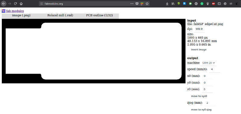
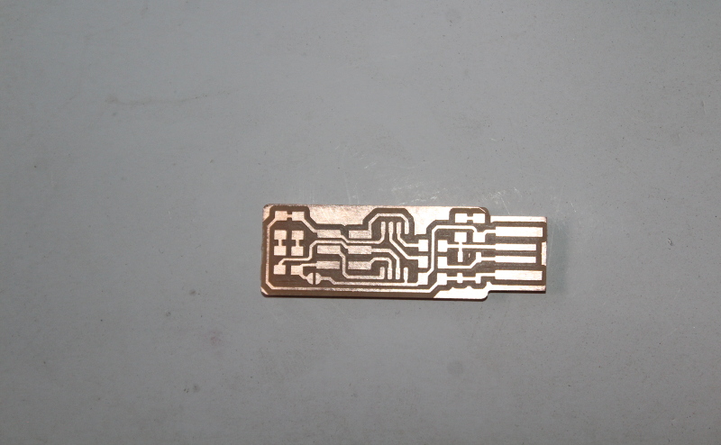
The following are images I used for milling the PCB.
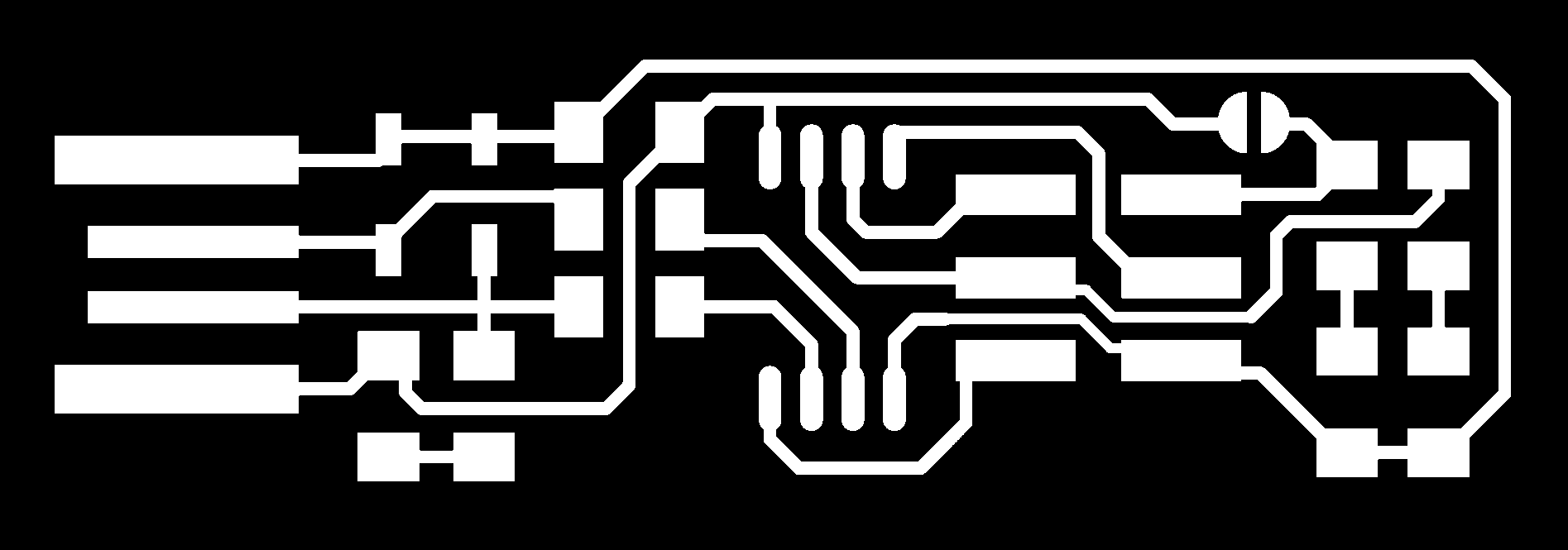
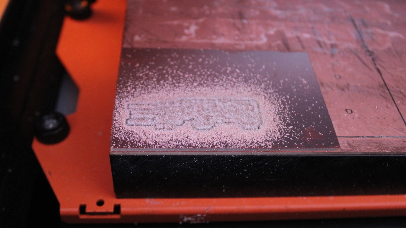
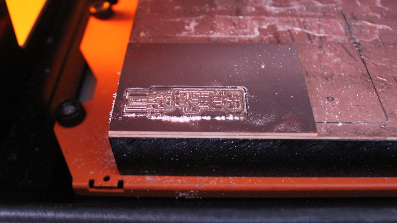
The above image is for traces for FabISP.

The above image is for edge cut of FabISP.
Set-up Milling machine and Milling PCB
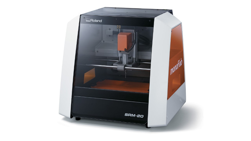
In FabLab Rwanda we have SRM-20 monofab milling machine.
In the milling machine there was a sacrifice board, since we use it some time.
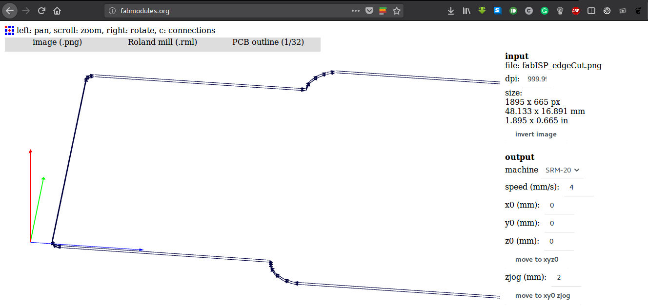
I have first converted my images from .png to .rml since its what the milling machine takes as input.
I used fabmodules to convert fabISP images to rml. On Input format drop down I choosed image(.png), on output format I choosed Roland mill(.rml), and on process I choosed PCB traces(1/64). And continued selecting on machine I choosed SRM-20, other settings were made automatically then I clicked on Calculate button for converting it.
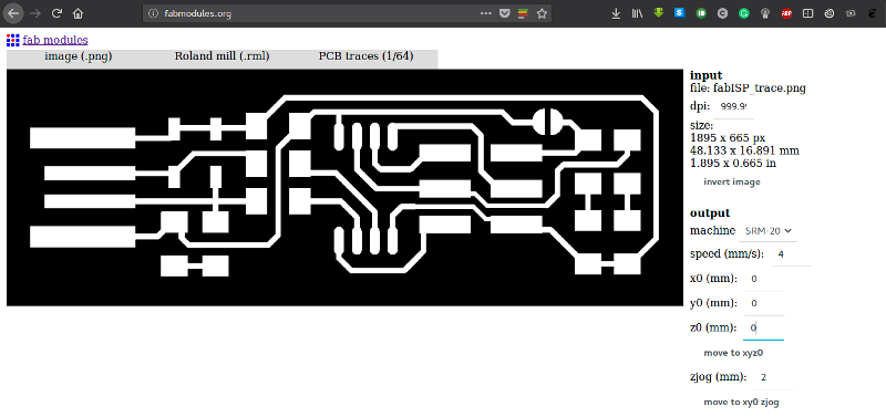
The image above shows some of the configuration I described above.
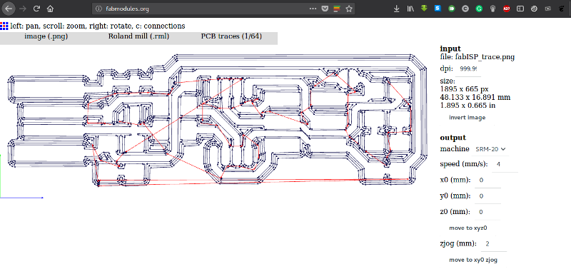
After calculation done on the image, the rml file is generated as shown above.
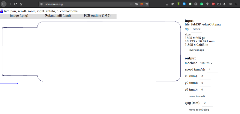
Now I have done the same thing on the edge cut file with some modification like on process I selected PCB outline(1/32) and on cut depth (mm): I entered 1.6 cause I want to cut through the board.
After calculating the path for the tool the RML file is generated.
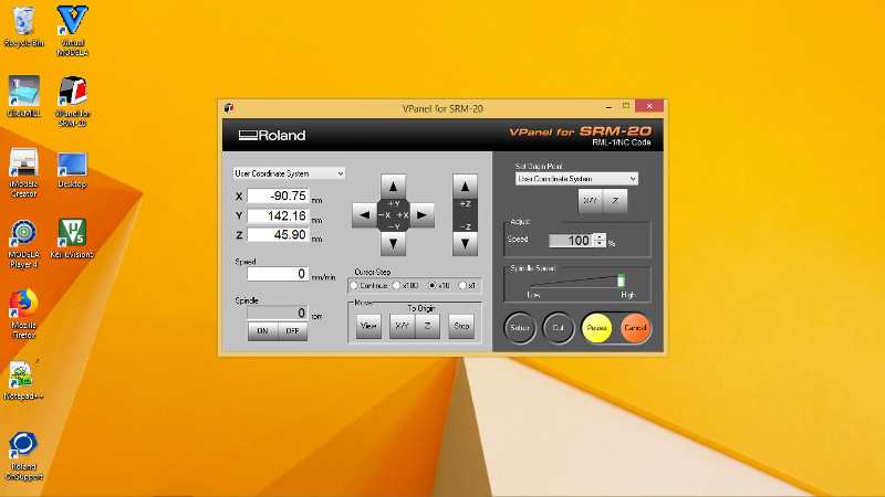
For now I had finished on converting the images and now what was next is printing the board. For printing the board I had to switch for Ubuntu to wndows because the software I use to communicate with the milling machine is windows based.
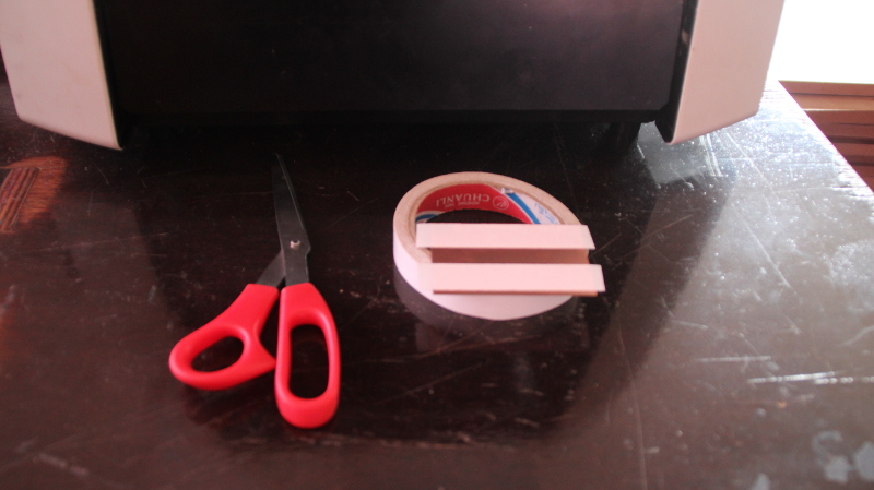
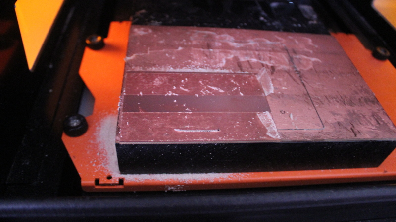
Now I taped on the back of the PCB and I using FR4 board(double sided).
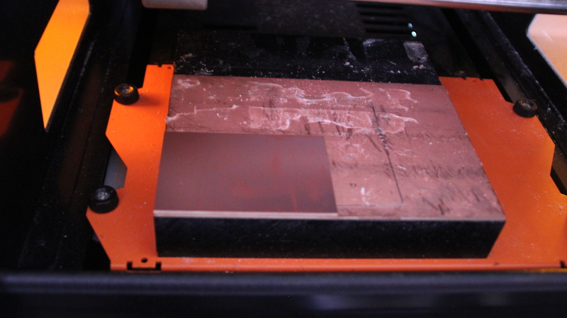
Now that I have fixed the board on the bed, I am ready to setup the machine and start milling.
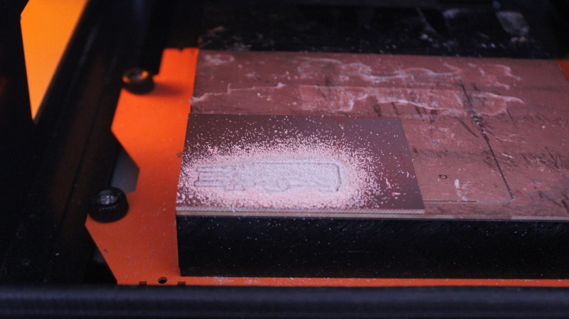
Now lets cut edge of the board we need.
while I was cuting the edges of the board, the machine started behaving weirdly. It started making many offsets more than what it was supposed to make.
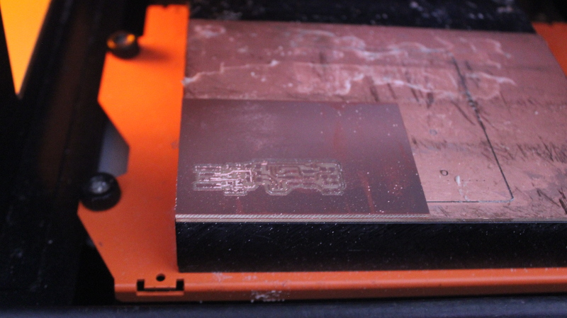
Here you can see how the board was lifted from the bed.
On this one you can see that the board wasn't cut through as it was supposed to.
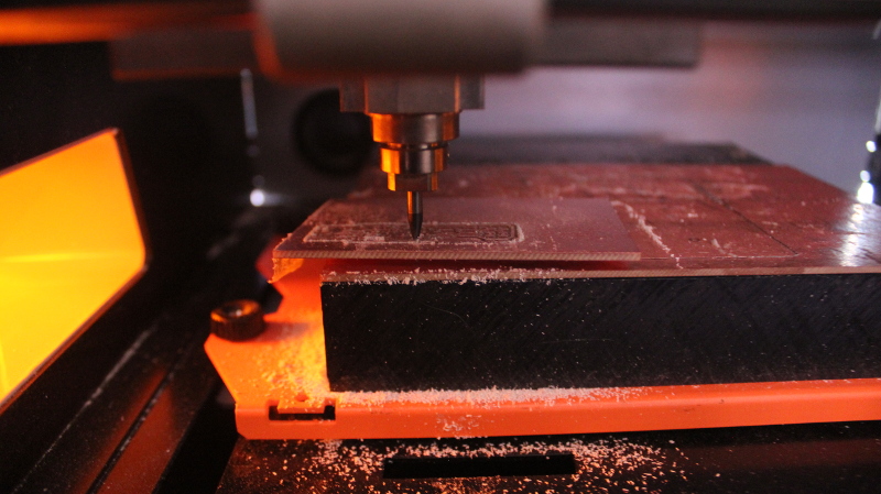
My board has totaly failed now I have to make another one. Now I have to go back and verify how the .rml file was created and if I didn't miss any thing.
I did make another .rml file for edge cut of the board properly, after the .rml file was generated I did zoom into the file and saw that 2 offsets were created.
The second trial it work fine without any difficulty.
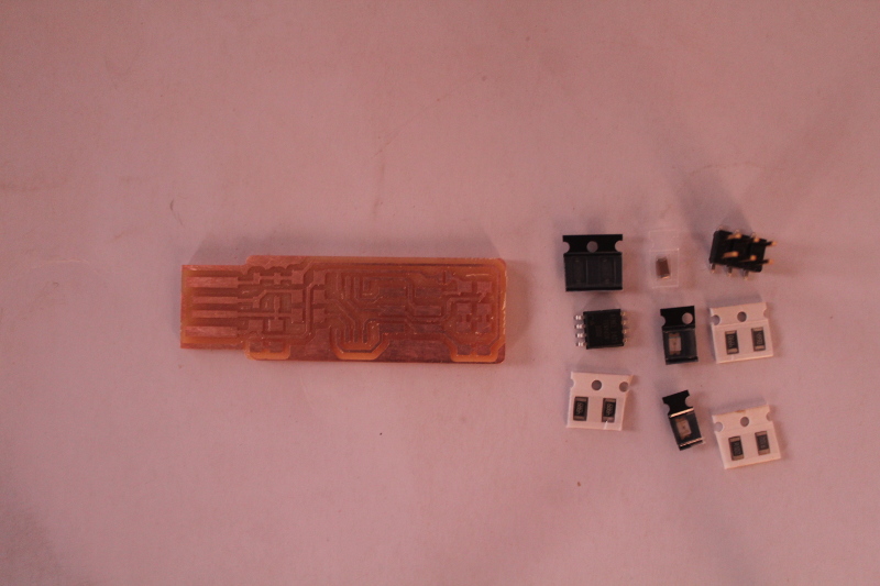
Assenbling the PCB
List of component used:
| No | Component | Pieces |
|---|---|---|
| 1 | ATtiny45 | 1 |
| 2 | 1 Kohm | 2 |
| 3 | 499 ohm | 2 |
| 4 | 49 ohm | 2 |
| 5 | 3.3 zener | 2 |
| 6 | Red LED | 1 |
| 7 | Green LED | 1 |
| 8 | 100nF | 1 |
| 9 | 2x3 pin header | 1 |
Now what follows is to solder all components to the board.
When I was soldering all components one of the component did get damaged because of the soldering which was too hot. But at the end everything was fine and looking great.
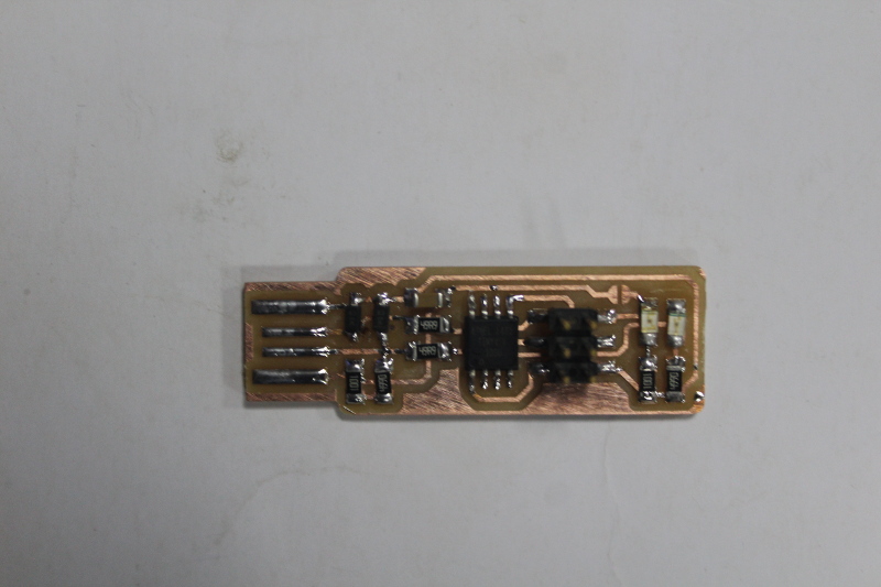
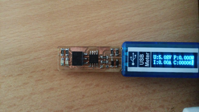
I check all the connection to the programmer with a multimeter for verifying that no misconnection or bad connected trace. After I connected the program on the computer.
Programming
First I downloaded the firmware to be loaded in the programmer.
Then run make flash in terminal to erase the target chip, and program the its flash memory.
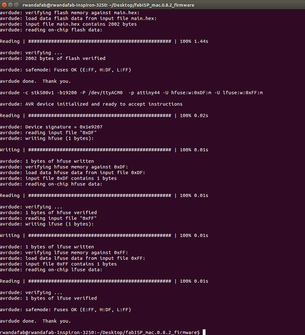 And run
 make fuses to set up all fuses except one that disables the reset pin. Before blowing the reset pin, I first checked if the programmer was visible to the computer by typing lsusb in terminal where the programmer was named Multiple Vendors USBtiny.
For blowing the reset pin, I typed rstdisbl.
After this process the USBtiny was ready as a programmer.
Conclusion
I am familliar with monofab, so I thought this assignment was going to be easy. Then when I was working I didn't pay attention on all details since I thought I mastered them, but I missed some steps and I ended up failing with the first PCB.
Additional from this assignment I also learned that no matter what is your experience with any of the machine its better to always pay attention on each step of your work.