ASSIGNMENTS
Group
use the test equipment in your lab to observe the operation of a microcontroller circuit board
Individual
- - Redraw the echo hello-world board
- - Add a button and LED (with current-limiting resistor)
- - Check the design rules,make it and test it
TOOLS and SOFTWARE
EAGLE Software
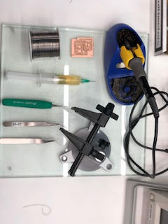
Rolland Milling Machine
Soldering Tools
Redrawing the Echo Hello-World Board
To complete this part of the assigment, I downloaded Autodesk EAGLE which is a software used in electronic design because it enables users to draw schematic diagrams, add components, PCB routing. Then, I did the following steps :
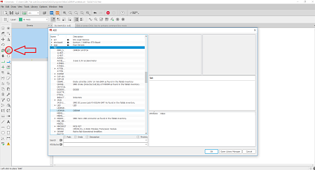
- 1- Fisrt things first, I downloaded the components library fab.lbr ,which is provided by Fab Academy, to my computer.
- 2- I created a new project by going to File in the top toolbar > New > Project > Rename the projec> Right-click the project you created > New > Schematic.
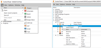
- 3- Now to add the library, I went to Library from top toolbar > Open library manager > Available tab > Browse > Select the fab.lbr file > Click on the library > Use and the library appeared in the list of available libraries.
The Schematic Design
- 4- Since I have already created the schematic in step 2, I went ahead and added all the components needed for the "Echo Hello-World" board by going to "Add Part" tool from left toolbar > Select the fab library and selecting the compnents I wanted to add.
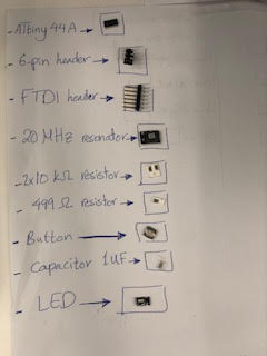
- The components I added are:
- Fab Library :
- 1- 1 x ATtiny44A (ATtiny44-SSU)
- 2- 1 x Capacitor (CAP-US)
- 3- 1 x 6-pin header (PINHD- 2x3-SMD)
- 4- 3 x Resistor (RES-US)
- 5- 1 x Resonator (Resonator)
- 6- 1 x FTDI 6-pin connector (FTDI-SMD-HEADER)
- 7- 1 x Button (6MM_SWITCH)
- 8- 1 x LED (LED)
- 9- 1 x Button (6MM_SWITCH)
- Supply1 Library :
- 1- Voltage Supply (VCC-Version 1)
- 2- Ground (CND-Version 1)
- Here's a picture of all the components I added.
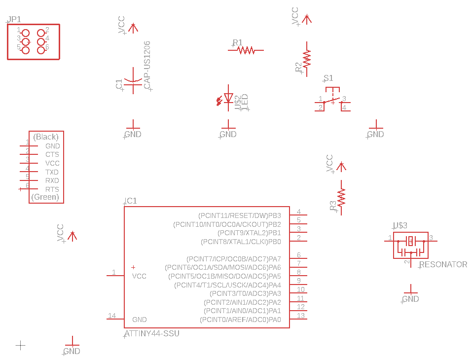
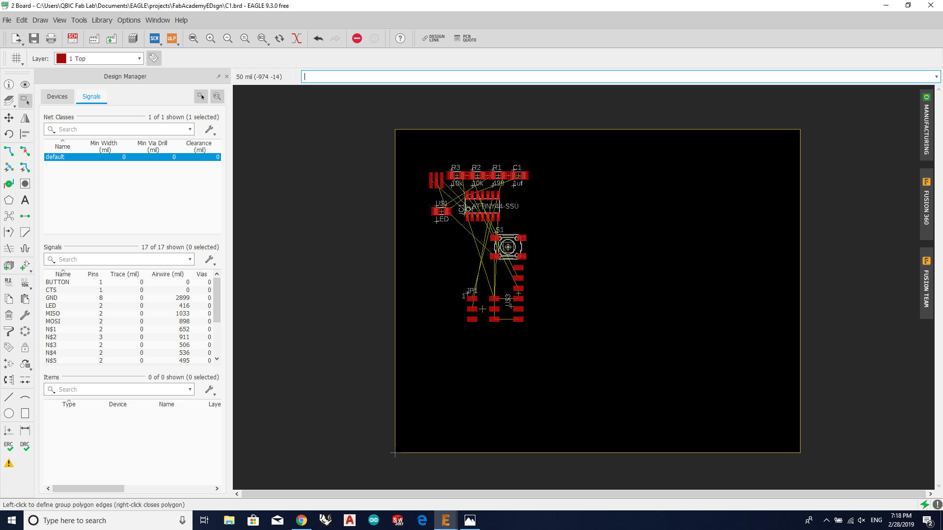
- 5- I started connecting all the components using teh "Net" tool from the toolbar on the left. To make sure that the schematic is clear and organized, I used the different editing tools from the left toolbar such as "Move" and "Rotate".
.png)
- For some connections, I just added a net/wire and gave it the same name as the components they should be connected to using the "Name" tool from left toolbar. This is another technique of connecting components.
.png)
PCB Borad
- 7- Once the schematic was completed, I genertated the PCB board using the "Generate/Switch to board" from the top toolbar. This will change the view to the PCB window in which the PCB layout can be designed, editied and finalized.
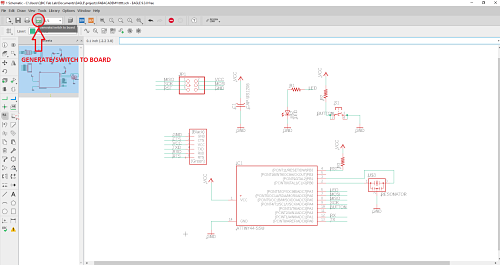
- 8- The generated board was on the left corner of the window, so I dragged it to the middle of the black area on the right using the "Move" tool.
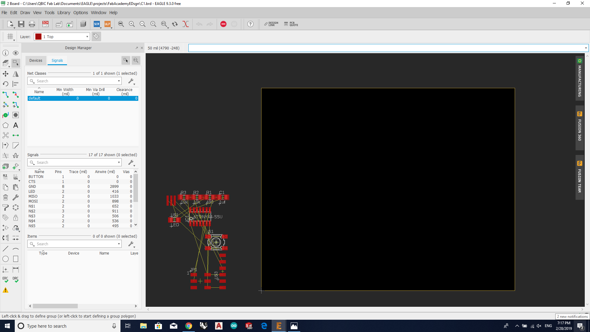
- 9- I started desiging the pcb by routing all the yellow connections using "Route" tool from the left side toolbar which will create traces. I used traces of widths 16 and 10 depending on where is the trace going.
- Notes:
- - when routing a trace, I made sure that it doesn't cross over other traces or too close to any other trace (clearance) because this might lead to problems such as short circuits when milling the board. (I learned this the hard way! :/ ).
- - Sometimes, I needed to edit a trace or redo it, so I used the "Ripup" tool from the left side toolbar to remove a trace or part of it.
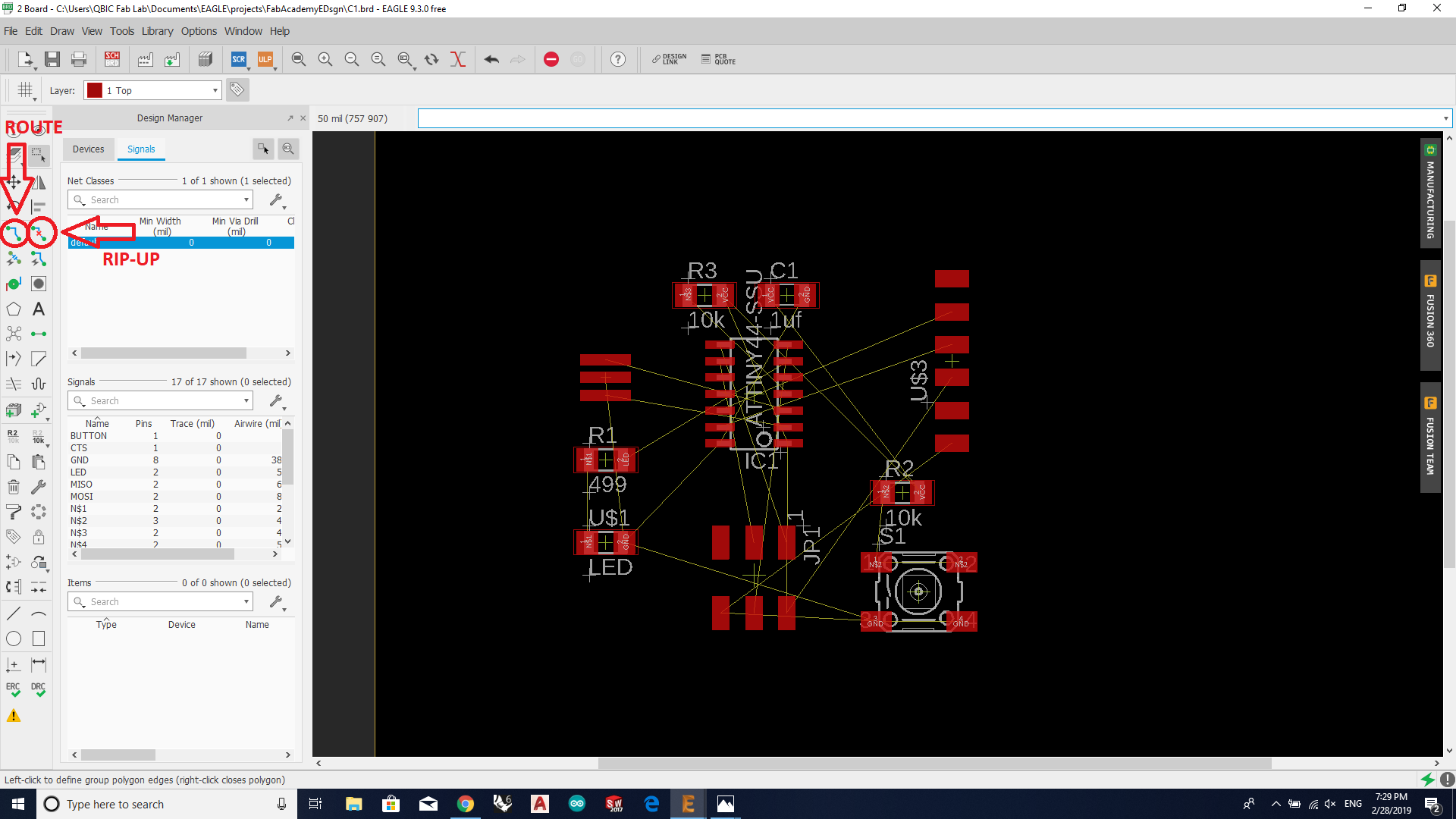
- Here's the final design after routing all traces.
.png)
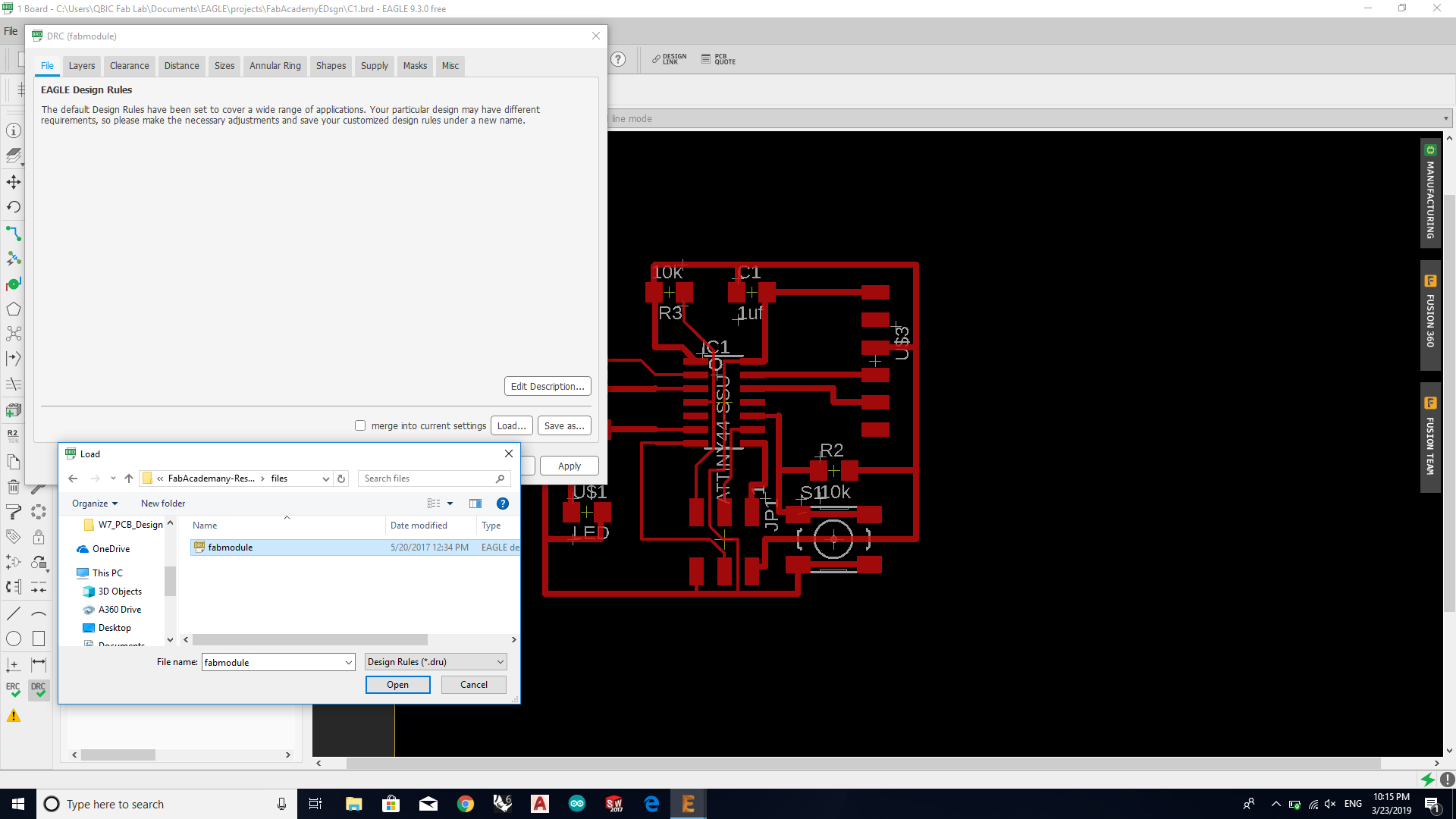
- 10- Now that I finished routing all the traces, I mooved to checking that all my traces are done properly. To do this, EAGLE has a feature that can check the design rules.
- To check the design rules, I needed to add the design rules script first. This script was in the same folder I downloaded in step 1 to get the library.
- 11- To add the script, I went to the top toolbar Tools > DRC > Load > Select the design rules file > Check.
- After the checking was completed, a window with some errors and warnings appeared. The errors were related to airwire which means the specified connections needs to be more secure.
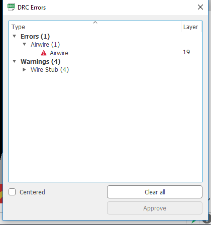
- I resolved all the issues and checked that the warnings are not a huge risk. Then, I re-checked the design again and everyhting was fine this time.
- 12- Now that everything looks fine, I prepared the board to be exported by going to the top toolbar then View > Layer settings > Select all layers > Hide layers > Select Top and Pads layers > Show layers > Ok
.png)
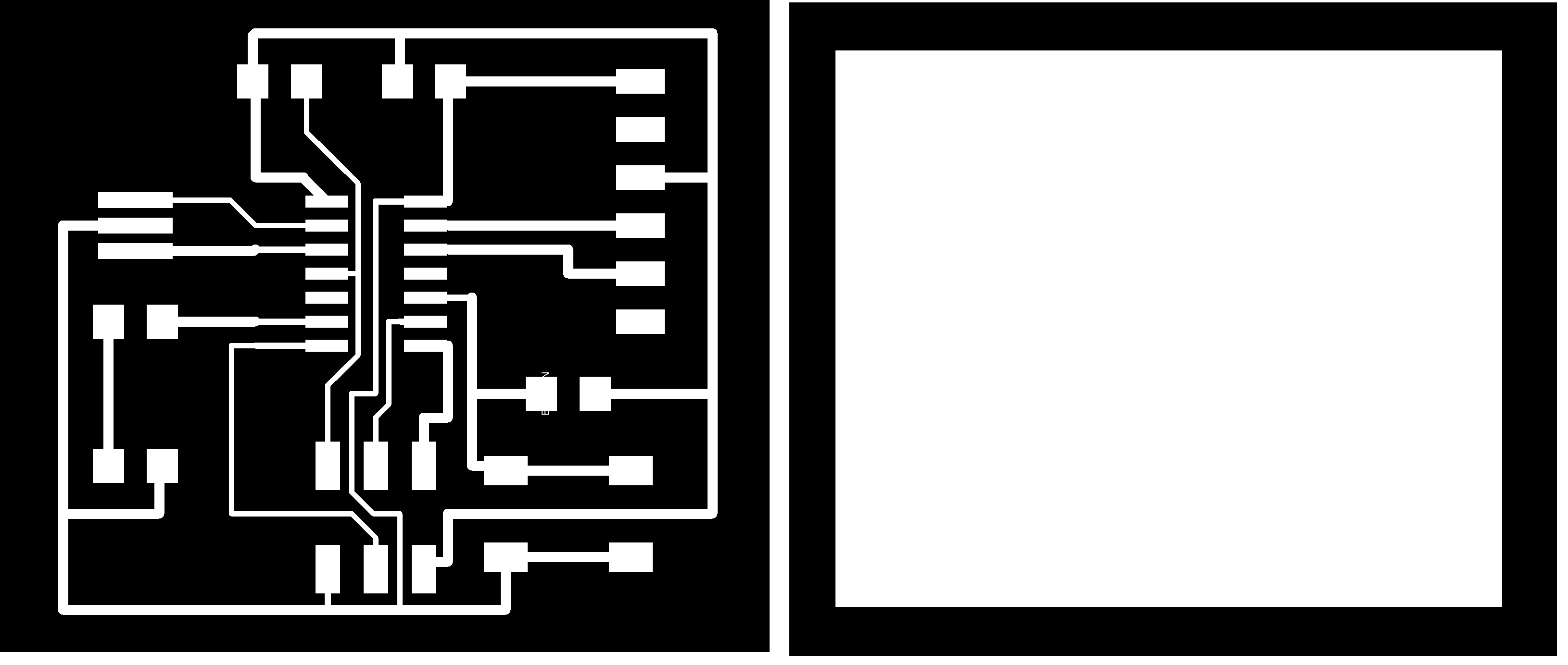
- 13- I exported the board by going to the top toolbar then File > Export > Image . Then, in the export window I did: Check Monochrome box > Set resolution to 1000 dpi > Set Area to full > Ok. The board design will be saved as png.
.png)
- 14- To draw the outline of the board, I changed the layer to dimension from the "Layer" dropdown in the top. Then, I used the "Rectangle" tool from the left side toolbar to draw a rectabgle on top of my board and I made it slightly bigger than my board.
.png)
- 15- I prepared the outline to be exported by going to the top toolbar then View > Layer settings > Select all layers > Hide layers > Select Dimension layer > Show layers > Ok
.png)
- 16- I exported the outline by going to the top toolbar then File > Export > Image. Then, in the window that appeared I did: Check Monochrome box > Set resolution to 1000 dpi > Set Area to full > Ok. The outline will be saved as png.
- The image below shows the final files after I exported and used an image manuplation software (GIMP in my case) to crop the exported images to the desired selection.
PCB Milling
- Before milling the board, the files need to be prepared. To do so, I used the Fab Modules web page.
- 17- In the fab modules page, I clicked Input format > Image and upload the board design I exported previously. Then, I changed the output format to "Roland mill" since the machine I used to mill was Rolland and I chose the process to be "PCB traces (1/64)".
- 18- I changed the output settings as shown in the images below.
- 19- I clicked in calculate and once it was completed, I clicked save which downloaded the file to my computer
- 20- I followed the same steps to prepare the outline file, but the output settings I set were a bit different as shown the images below.
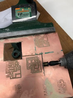
- We're finally ready to mill !!
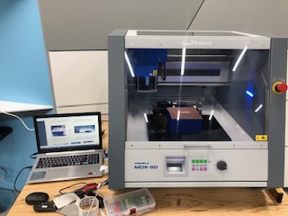
- I used the Rolland MDX-50 to fabricate my board. I followed the same steps from Week 5: Electronics Production assignment. However, milling this board was not as easy as I expected because I faced some challenges while milling and I did multiple trials until I was able to mill it successfully.
- Trial 1:
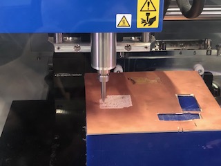
- In this trial, I didn't use the 1/64 bit to mill but instead I used a tool called V-tool which is a milling tool that comes with the machine because the 1/64 bit was broken and I didn't find another one. As shown in the picture below, the board may look good at first sight, but I noticed there were short circuits. My interpretation is that the V-tool isn't able to mill accurately when it comes to traces that were relatively close and I noticed that some of my collegues faced the same issue. Therefore, to resolve this issue, I got the 1/64 tool and used it in the seconde trial.
- Trial 2:
- This time, the board came out wih one side that was not milled and there was still copper left. I consulted with one of the Fab Engineers and according to her this problem was due to the leveling of the sacrifice board (The blue wax block). Hence, I replaced it with another block and things looked fine this time.
- Trial 3:
- The issue with this trial was that the machine did the milling properly but when it was time to cut the outline, it cut the outline in the middle of the PCB. I assumed it was a calibration error so I calibrated it again
- Trial 4:
- This time the milling was perfect and again when it was time to cut, the machine was going to cut part of the trace again but I was able to pause it before it does that (Phew!!) and consulted with the Fab Engineer and we found out that there was a problem with the machine.
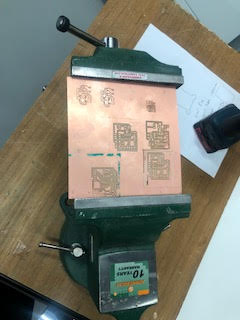
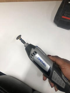
- Finally, I decided to cut the outline manually because I was running out of time and the machine needs time to be fixed. Thus, I used the Dremel power tool shown below to cut the outline and sand the rough edges.
- I was finally able to fabricate my board
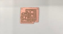
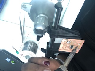
Soldering Components
- Finally, I collected all the components and placed these components on the board. I used the same technique I followed in Week 5 : Electronics Production to solder.
- The only challanege I faced during soldering was that I realized that I broke a trace while cutting the board manualy. It was a bit difficult to bridge that gap with solder so I used a 0 ohm resistor to close the gap without affecting my board.
- Here is my final MASTER PIECE !!.