Exercise 4. 💾 Electronics Production ⏳ (Challenging exercise 😅)
At the end of this exercise, I should be able to:
1. Characterize the "design rules" such as: A)Feed; B)Speed; C)Plunge Rate; D)Depth of cut(traces and outline); E)tooling; for printed circuit board (PCB) production process.
2. Document and describe the workflow of milling PCB.
3. Make an In-Circuit Programmer (ICP)/In-System Programmer (ISP) by milling and suffing PCB and then test it.
4. Describe the process of A)Milling; B)Stuffing; C)De-bugging; D)Programming.
PCB is is an electrical circuit whose components and conductors are contained within a mechanical structure. For FabAcademy. The conductors are made of copper layers on one side of the board and the components are mostly Surface Mount.
The below articles are very useful for an electronics noobs like me that just getting started:
https://hackaday.com/
https://www.digikey.com
https://www.instructables.com
Characterizing PCB Production Process such as document feeds, speeds, plunge rate, depth of cut (traces and outline) and tooling. (Group Work)🛠⚒
This exercise was done together with Ting Kok Eng and Yeo Gau Siong using the STEPCRAFT D.420 in T14 level 4 Fab Lab of Singapore Polytechnic.
The details of the steps can seen HERE.
The summary of the steps are below:
The first process in making PCB is to design PCB using Electronics Design Automation (EDA) softwares such as EAGLE.
In the EDA softwares, schematic drawing of the circuit will be made by the designer to define the circuit and components.
With this schematic drawing, a board layout will be created, where the designer will organize the components and route the circuit following the design rules.
In exercise 4, the design process is omitted and a board layout is already given hence I only need to use the board layout given. This is why this week exercise is called Electronics Production, not Electronics Design.
Using the board layout drawing, a G-Code will be created using softwares. This G-Code contain mathematical vectors for the milling machine to work to provide precision.
In this exercise, I will use mods created by Neil to create the G-Code from the board layout drawing(.png file)
After the milling is done, now I have to stuffed the components (Surface Mount) onto the board by soldering.
And that's it, now the the electronics is ready to be programmed where the code will be uploaded into the microcontroller and then tested.
If it doesn't work, de-bugging process must be done.
Personal reflections in characterizing the PCB production process😎
(1) The offset in the mods is NOT for milling deeper (z direction). It is for milling wider (x and y directions). Options set in mods: (a) offset number (how many times) and (b) offset stepover (recommend to use 0.5 which 0.5 of the tool diameter)
(2) To have different passes and deeper mill depth, the setting used is the cut depth and max depth. Max depth/cut depth = passes on the z direction.
(3) To make the milling process a bit faster, the options use are: (a) cut speed = 50 mm/s (b) plunge speed = 50 mm/s. Else can use the default values which are 20 mm/s. Values higher than 50 mm/s are not recommended because the milled result will be rough.
Making In-Circuit Programmer/In-System Programmer (ISP)🛠⚒⏳
The processes in making the in-circuit programmer/in-system programmer (ISP) is listed below:
1. Designing the circuit board (OPTIONAL) using EAGLE software.
2. Milling The Circuit Board
3. Stuffing the PCB
4. Testing the continuity (workflow instead of process)
5. Programming by installing softwares on PC, setting firmware, and uploading code onto the board.
6. De-bugging
In-System programming (ISP), also known as in-circuit programming (ICP), in-circuit serial programming (ICSP) allows programming and reprogramming of microcontrollers, already soldered on a target PCB.
Microcontrollers like AtTiny that connect to input devices and/or ouput devices are typically soldered directly to a printed circuit board and usually do not have the circuitry or space for a large external programming cable to another computer, hence it is beneficial to have ISP.
ISP on Wikipedia page.
1. Designing circuit board using EAGLE software (optional)😎
For this exercise, I attempted to re-design the ISP that was designed in this page by Brian.

I wanted to immediately learn to use EAGLE software instead of directly using the board drawing for traces and outline given as .PNG files which I can esily generated the Gcodes using mods.
To learn how to use EAGLE, I used sparkfun tutorials and download the fab library.
Below are the steps to start new project in EAGLE:

Below are the steps to add the fab library to the EAGLE library. Note that the default EAGLE library has many components, while fab library contains few but specific components for the use of this course. Hence I only use the fab library and remove the EAGLE library.


But I stopped using the EAGLE after attempting to create the design because I have not understand the circuit, schematic and board layout etc. I will attempt again in week 6 Electronics Design.
2. Milling the Circuit Board🤨
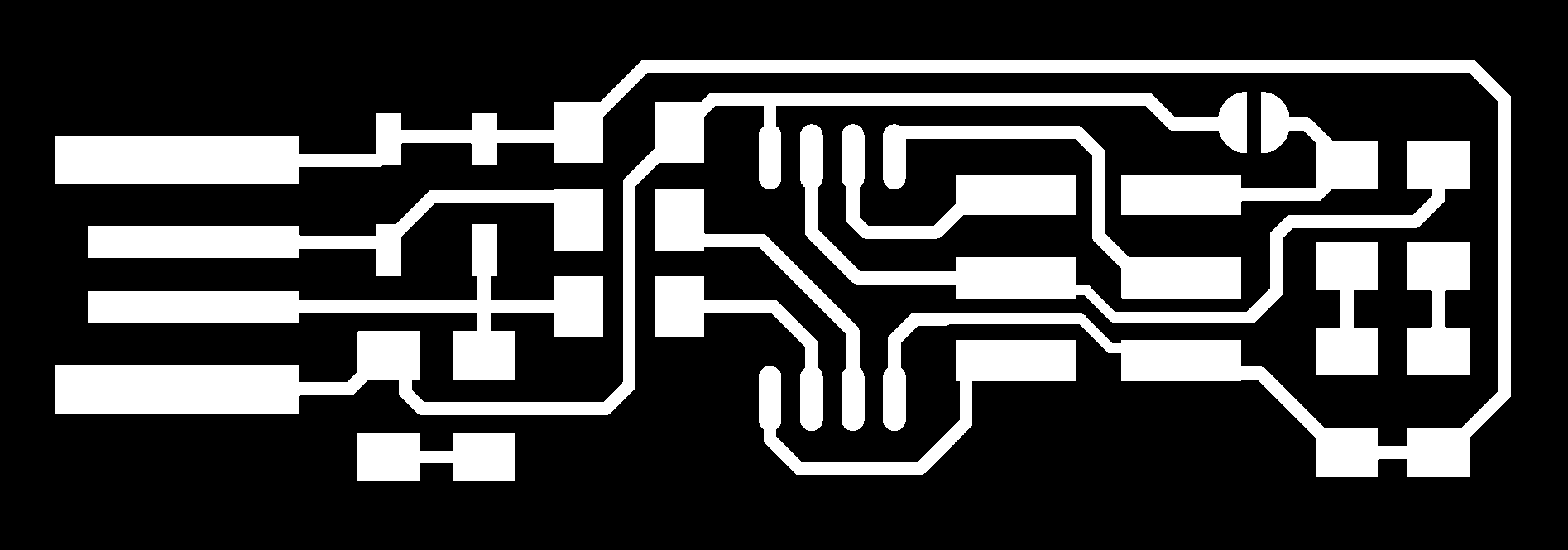
Using the PNG file for the traces milling provided as shown below,I used the mods to set the G-code.
 The end mill used is V-shaped 0.1mm 10degree.

Setting in mods for the trace milling (see below picture): 1 pass is when the cut depth = max depth = 0.06 mm to mill off the cooper from the board. 0.06 mm is the thickness of copper on the board from the surface. Under the “path to G-code”, the cut speed can be set to 50 mm/s to make the process faster.

Simulate the GCode using CAMotics:

Setting in mods for cutting the board: Using the PNG file for the outline cutout provided as shown below, I used the mods to set the G-code.
 The end mill used is flat-shaped 0.8mm.

Setting in mods for the outline cutout (see below picture): 4 pass is when the max depth (1.67 mm) = 4 times the cut depth (0.42) mm to cut the outline of the board. 0.06 mm is the thickness of copper on the board from the surface.
 Simulate the GCode using CAMotics: the 4 passes that go deeper can be seen in the below picture
 The board produced after milling:
 After sanding the burr and peeling the outer part of the copper for the usb:

3. Stuffing and Soldering the Surface Mount Devices (SMD) onto the PCB😣
These are the surface mount devices to be soldered onto the PCB
 This is my first time soldering such tiny devices onto PCB and I have to unlearn and learn the correct way of soldering. Thanks to Gau Siong, Rodney and Steven for patiently teaching me the correct way of soldering.
Half way into soldering the smd, I was advise it’s easier to do soldering if the dead copper is removed from the board, hence I removed almost all the dead copper by using sharp penknife by scrapping it and gently pulling out the scrapped part. Below are the results after I removed all the dead copper and soldered all the SMDs.


4. Testing the Board Continuity
After physically checking the soldered parts and compared to the schematic and PCB layout image, I did the checking of the continuity using multimeter (Sanwa digital multimeter CD800a).

5A. Softwares installation for programming the FabTinyISP😣
I followed the steps mentioned in this Brian's page starting from:
 (1) Download and install GNUMake (make-3.81).
 (2) Download avrdude-win-64bit.
(3) Unzip the archive and copy the folder “avrdude” inside C:\Program files
 (4) Download avr8-gnu-toolchain-win32_x86 and copy the folder inside C:\Program files too.
(5) Update the path in “Control Panel” > “System” > “Advanced System Settings” > ‘Environment Variables” > Edit and browse and add 3 new paths as shown in the below picture.
 (6) Download Zadig and launch it.
5B. Get and build the firmware
Download the firmware and extract it to the same folder as your git-bash parent directory (see picture below). My master directory is noel-kristian and the parent directory is fabacademy.
 Run git bash and change the directory to fts_firmware (shown below) and type command “make”.
 This command will create 2 new files (.elf and .hex) inside the fts_firmware folder.

5C. Programming the FabTinyISP😣
Now, the board is ready to be programmed. The board is connected to a programmer and connected to a laptop as shown below.
My board now is called target where it will be programmed by the programmer attached to my laptop. Command prompt environment will be used for this exercise.
 In the command prompt, change the directory to where the fts_firmware is located and type command “make flash”. This will erase everything in the new programmer board and make the machine code (.hex) to be uploaded to my board (new programmer board)
 After that type command “make fuses”. This will configure the fuses on my board (new programmer board) according to the machine code.

 After this step, we need to check whether the new programmer board (my board) can be recognized by PC by connecting it directly through USB port as shown below:
 But my Windows PC can’t recognized the USB as shown below:

6. De-bugging😣
The “make flash” and “make fuses” commands were successful, hence the new board is already programmed as programmer.
But when it is connected to the PC, PC can’t recognized it, likely the reason is the connections due to soldering of the SMDs between USB and the microcontroller (the 2 resistors near usb, 1k and 499 ohm, the two zener diodes and the two 49 ohm resistors).
 Rework was done on all these SMDs and afterwards the board is connected to PC again and now it can be detected by the PC under “device manager” as libusb-win32 devices -> USBtinySPI as shown in picture below.
 Since now my board as a programmer can be recognized by the PC, the next step is to execute the command “make rstdisbl”. This command will disable the reset fuse so that the board can be a full programmer.

 The next step is to test my board as a new programmer by connecting it to a target board (t45). When they are connected, the 2 LEDs on my board are on (red and green), indicates that my board is communicating with the PC and with the target board (t45).
 After which I execute the command “avrdude -c usbtiny -p t45 and the command was executed successfully.
