Exercise 6. ⏳ Electronics Design 😣 🦅 🙂
At the end of this exercise, i should be able to:
1. Observe the operation of a microcontroller circuit board using multimeter and oscilloscope amd document it.
2. Re-design one echo hello-world board by adding at least a button and LED using EDA software.
3. Make the above board and test it.
This exercise is the continuation of Exercise 4. Electronics Production. But this time, I need to design the board myself using EAGLE software.
EAGLE is a scriptable electronic design automation application with schematic capture, printed circuit board layout, auto-router and computer-aided manufacturing features.
EAGLE stands for Easily Applicable Graphical Layout Editor, so it is not an animal just like what Ting said.😅
Observe the operation of microcontroller circuit board using test equipment (group assignment)
This exercise was done together with Ting Kok Eng and Yeo Gau Siong.
The details of the steps can seen HERE.
Re-design Echo Hello-World Board (add a button and a LED), make it and test it
The processes to make the Echo Hello-World Board is listed below:
1. Drawing/designing the schematic and board layout using EAGLE software.
2. Milling the circuit board and stuffing it.
3. Programming the board.
1. Drawing/Designing the Schematic and Board Layout using EAGLE software🦅🕊
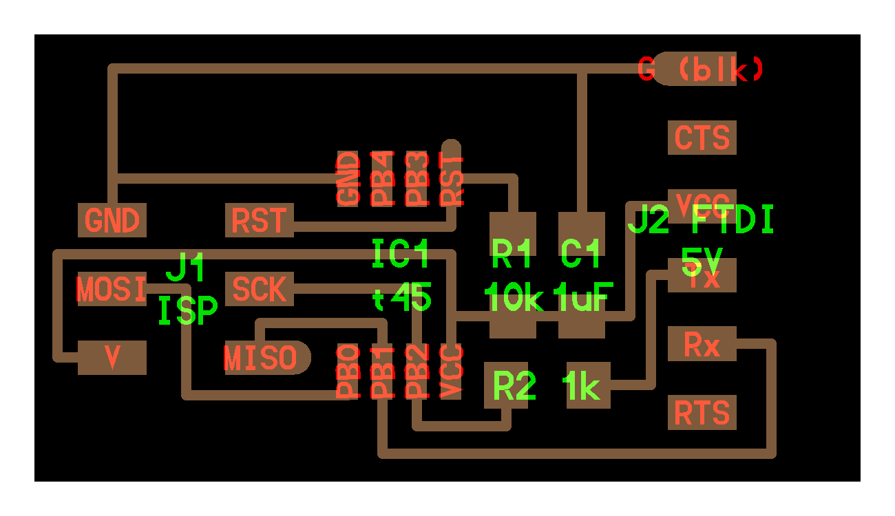
For this exercise, I selected to redraw ATtiny 45 and add one button and one LED. Below is the ATtiny 45 board before the button and LED were added.
 To program the ATtiny 45, an ISP (In System Programmer) connector is required. This is a 2x3 header. The ISP board was made in exercise 4. To provide connection to other target, a 6x1 FTDI header connector is required.
A current limiting resistor for LED is a must, otherwise too much current will flow through the LED and shorting it. For this purpose I used a 10k ohm resistor. For push button, I will use external pull-up connection as shown below.
 In this exercise, I continued to use EAGLE software. How to start using it can be seen in week 4 exercise.
To draw the schematic and board layout, EAGLE is used. At first, it was a foreign interface and lots of exploring was done to familiarize with it.
I relied heavily on the sparkfun tutorials and FabAcademy tutorials such as:
How to read a schematic
Schematic tutorial
Board layout tutorial
Below are the steps to draw the schematic in EAGLE:
 The library used for this exercise is fab library. Refer to exercise 4 on how to add fab library into the default library.
Below are the steps to add the parts:
1. Adding the microcontroller (ATtiny 45)
 2. Adding AVRISPSMD
 3. Adding FDTI-SMD-HEADER
 4. Adding 3 x RES-US1206
 5. Adding CAP-US1206
 6. Adding LED1206
 7. Adding 6MM Switch button
 The schematic result:

After adding all the components and connecting them, now it’s time to create the board by following the picture below.
 After moving all the components into the drawing area, I selected to use autorouter since this is my first time designing a board.
Before selecting the autorouter, we must first set the Design Rules.
Check (DRC) where we can set the gap between traces to 12 mil (12/1000 inch) and traces width to be 12 mil too. See below:
 After which, we can select autorouter and we must select “*” as shown in step 2 in the figure below, this is to ensure the autorouting is done from all side.
In my first attempt, there were 4 options as the result. Only the 4th option produces 100% free of errors. Option 1, 2, 3 only achive 95.2% where they have errors (likely air wire).
 After reviewing the 4th option, I decided to rearrange the components on the board and try autorouting again and do manual adjustment by using “ripup” and “route airwire” commands.
Below is the final board layout ready for milling.

2. Milling the board and stuffing the board🖋📌🕹
To make the board, I decided to use mods to generate the g-code just like in exercise 4. Before that I need to generate the png images from the board layout in EAGLE. Below are the steps to export the trace image to png file for mods:
 For the cutting of the board the option selected is not top but milling as shown below. The rest of the steps are the same as trace image.
 To generate the gcode, I use mods. Below is the setting I used in mods for the trace.
 The result:
 I peeled out all the dead copper and then stuffed all the components onto the board. The result:
 I have become better in soldering compared to exercise 4 🤩
3. Programming the Board💻
To program the board, I will be using Arduino IDE. To use Arduino IDE to program our attiny45, I followed this tutorial. This is important because Arduino board is different from ATtiny board hence there should be additional steps.
 After installing Arduino in my windows PC, I followed the below steps:
 Setting the correct board to Attiny45
 To program the board, I use the default examples given in Arduino, namely “Blink” and “Button”
 I modified the original code “Blink” program to suite the number of pins in ATtiny45. I replace LED_BUILTIN with PB1. This is because I connect my LED to PB1 (pin #6).
 Connecting the ISP programmer that I made in week 4 and my ATtiny echo-board to my PC:
 To execute the program, I followed the below steps:

And it works
To test the button, I used the default “Button” and modified according to my board pin number. I connect the push button to PB0 and LED to PB1.

And it works
Lesson learnt in milling:🙈
Always visually checked the end mill and compare with the rest. I used a broken end mill and as the result, almost all my traces were cut-off. I wanted to use V-shape 0.1mm 10 degree angle. But the one that I used had a broken end-tip as shown below. It took me almost 3 hours of milling then realize that the cause is the end-tip.
