Electronics design
Week 07
Like every week I started the week planning the assignment.
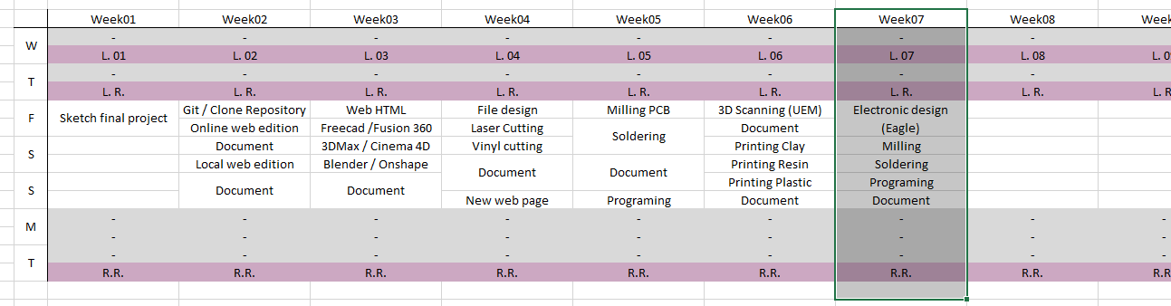
Group assignment. Characterizing the machines
I am a remote student and none of my colleagues are in the fab academy, so I did this part of the assigment individualy.
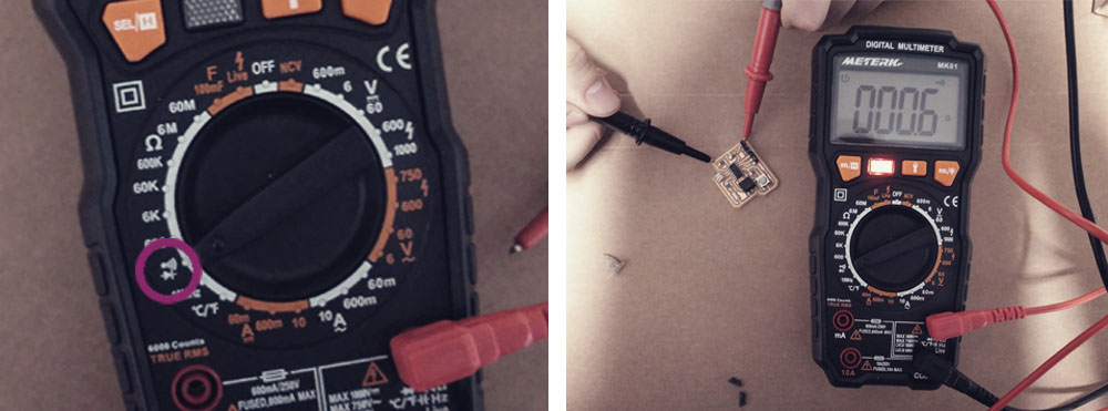
This is my new best friend: the multimeter. I use it to check the continuity in the PCB. And I use it all the time. I set a component and I check that there is continuity. That gives me confidence and allows me to check that the component is good soldered.
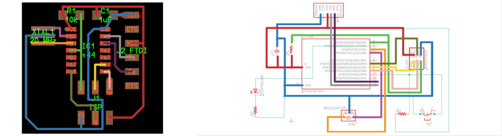
Designing the electronic circuit with Eagle
I decided to use Eagle for this assignment. I had never work with it so our instructor gave us a class/tutorial to know the basic commands so we could start as soon as possible redraw the echo hello-world board.
First of all I downloaded the “fab library for Eagle” where you can find most of electronic components that you will use during the fab academy. Then I created a new project and a new schematic into it so I was ready to started working. The first thing that I did was to add all the necessary components for the hello-word board and the extra button and LED (and its resistors), being very careful selecting the correct packaging and footprint.
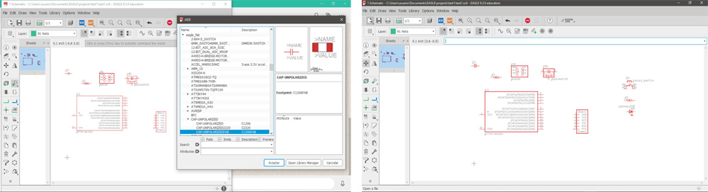
When I had all the components I created the connexions between them using the net tool. During this process I was also using all the time the tools move, rotate and delete to redraw the position of the components and connexions, in order to have a scheme as organized as possible.
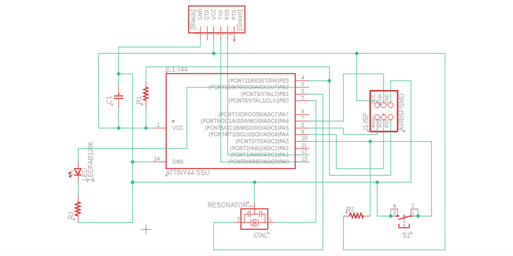
Then I checked that everything was correctly connected. I used a colour code to follow the paths so being sure that all connections were checked.
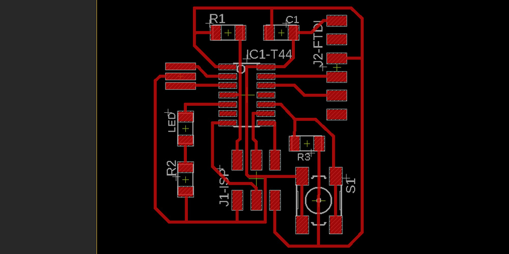
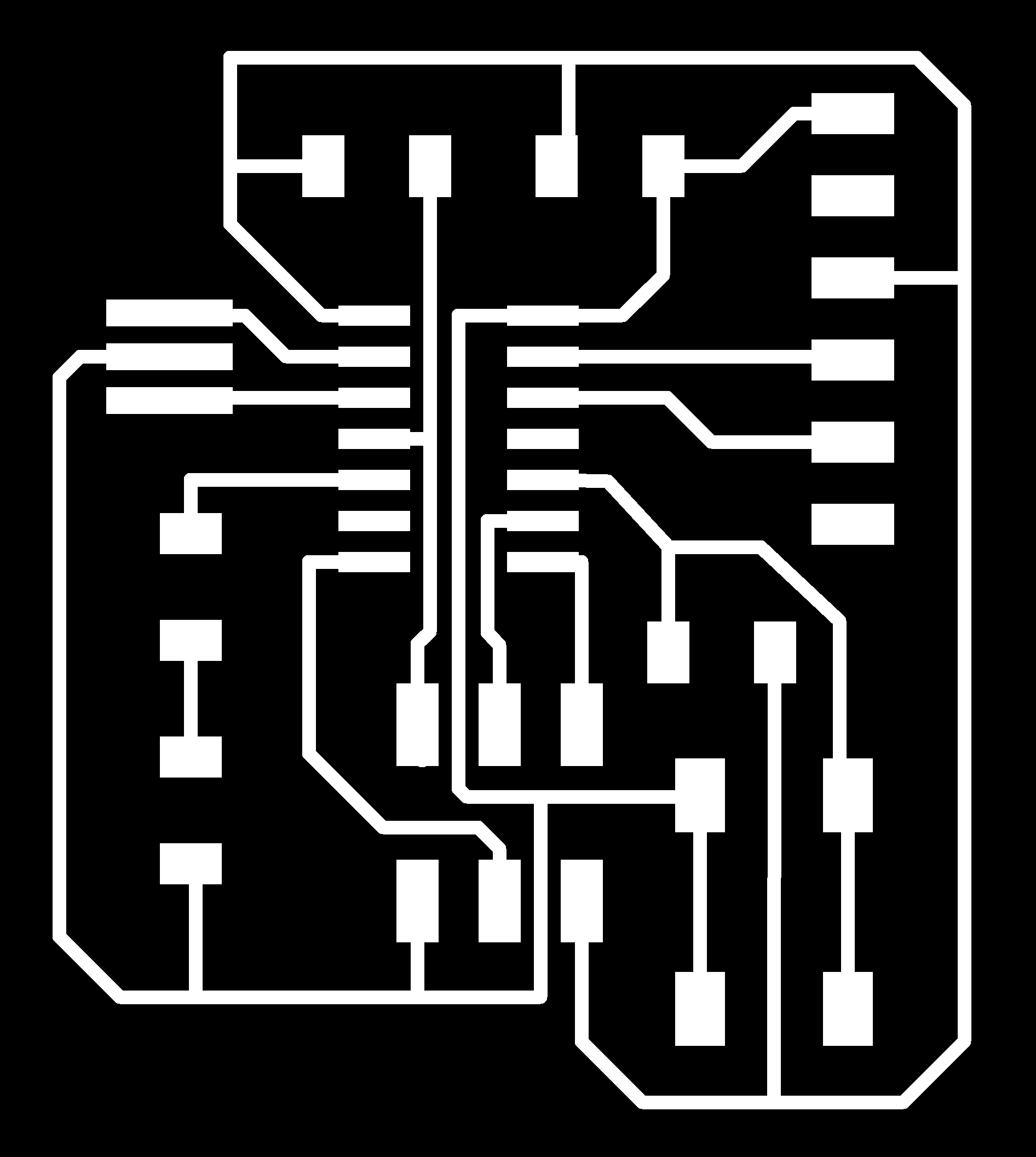
Once this was done, I opened the board window, where we can design the PCB. The first thing that I did here was to load the design rules (.dru file) included in the Eagle Library in GitLab. To do that, I went to edit > design rules > load and then I checked that I had 16ml for the size of the paths and also 16ml for the minimum distance between paths (clearance). Then I arranged all the components on the PCB board and I drew the paths using the route command.
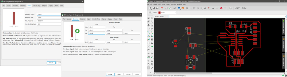
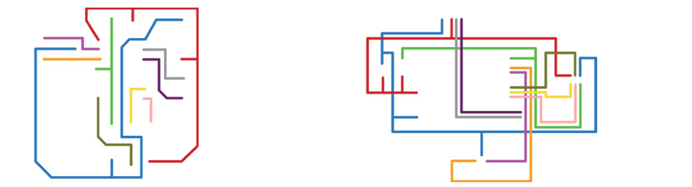
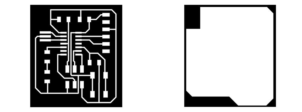
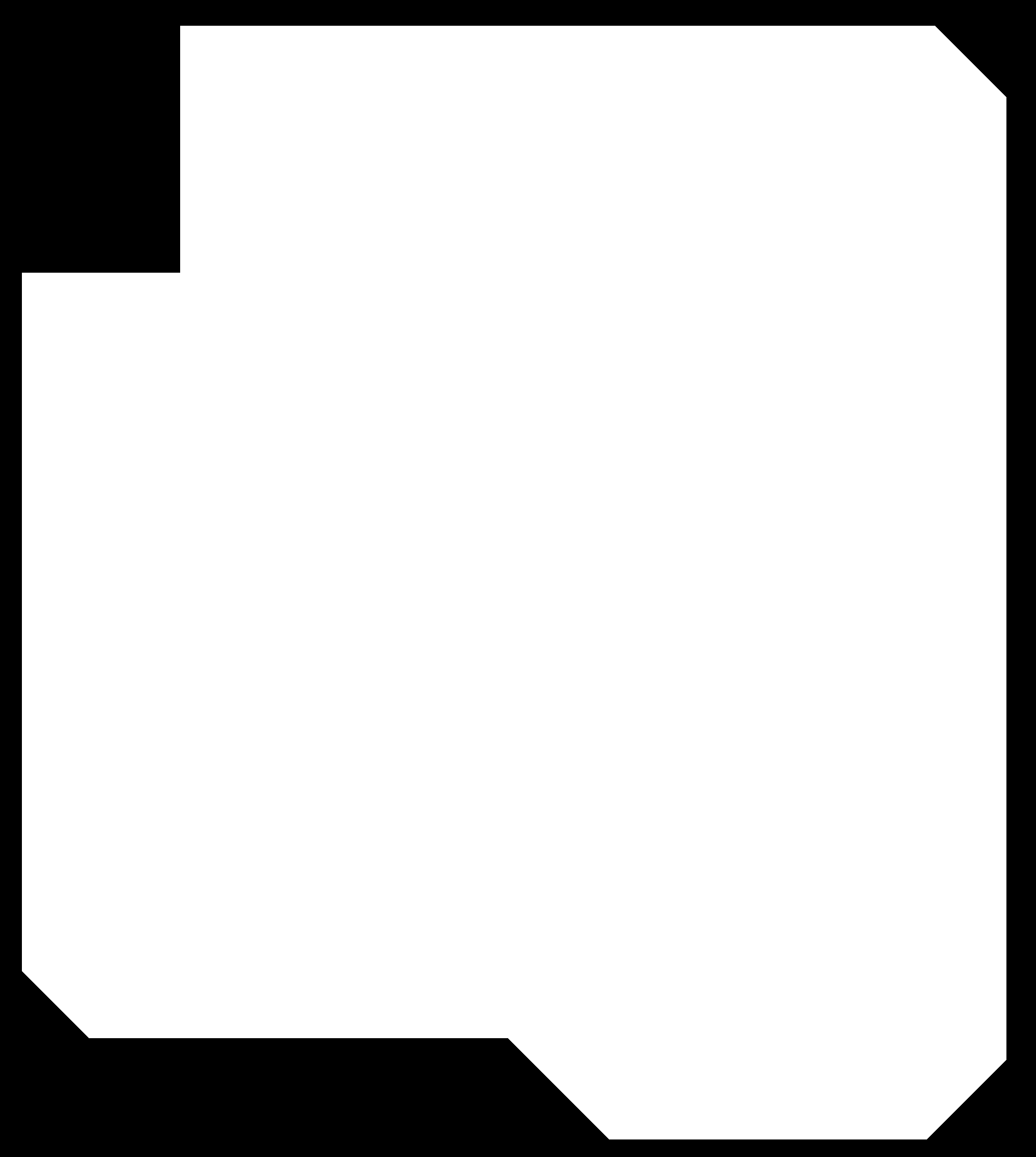
Then from tools > errors I checked that everything was well connected. Everything was ok, excepting for some warnings telling that I haven't specified the values of the capacitors and resistors, but all connections were good, so I exported the board into image choosing monochrome and 1500 dpi for the resolution. Then in Photoshop, I trimmed the .png and I created the image for the outline. To do this in Photoshop, I opened the .png file and first of all I used the trim tool to reduce the area of the image without changing the size, just cutting the part of the image that I didn't need. Then, using the polygonal lasso tool, and helped by the rules in the edged of the window, I created a polyline around the traces and then I erased the image inside this polyline, getting the image for the outline.
I found this process very amusing, finding the better place for all the components keeping in mind their paths. It is similar to play Tetris XD. I liked it. I enjoyed it a lot.
Creating the .rml files with Fab Modules
I used Fab Modules to generate the .rml files for milling the PCB applying the same settings that use when I milled the board for the FabISP.
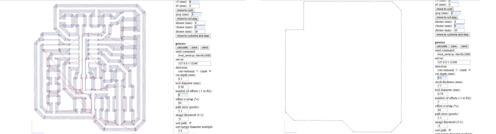
For the traces I had to trick the software and I set 0,38mm. for the tool diameter, otherwise if I keep 0,4mm. some of the spaces between paths are ignored.
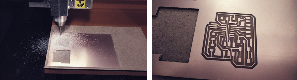
Milling the PCB with Roland MXD-40
I milled three copies of the PCB, just in case.
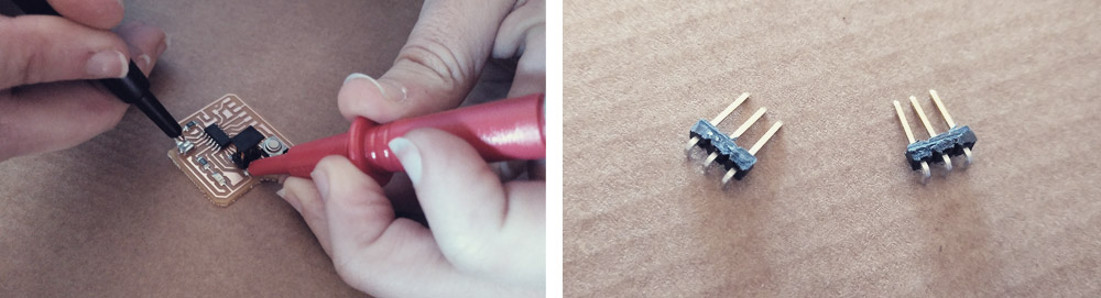
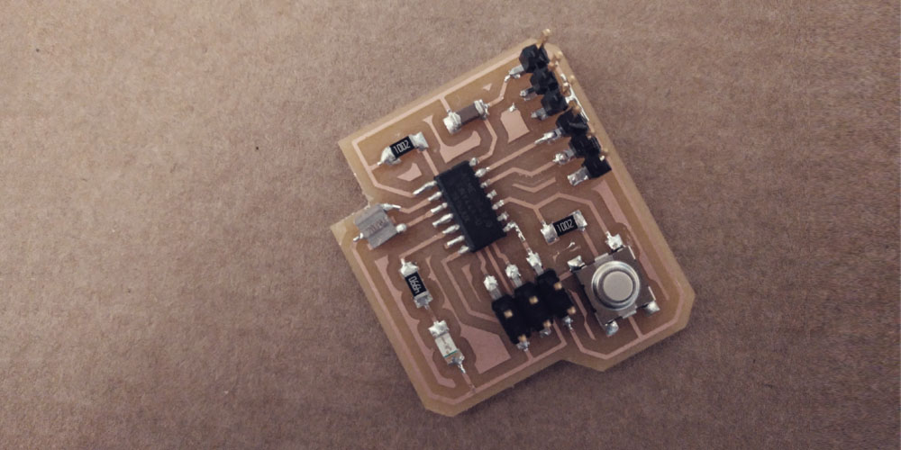
Soldering the components
The electronic components that I used for this assignment are:
> 1 x ATtiny44
> 2 x 10kΩ resistors
> 1 x 499Ω resistors
> 1 x 1uF capacitor
> 1 x 20MHz resonator
> 1 x 2x3 pin header (ISP)
> 1 x LED
> 1 x Switch
> 6 x Male headers
While soldering I checked with the multimeter that all connections were well done.
For some reason when I ordered my electronic components I forgot to ask for some male headers, but I solved that problem cutting one 2x3 pin header in half.
Programming
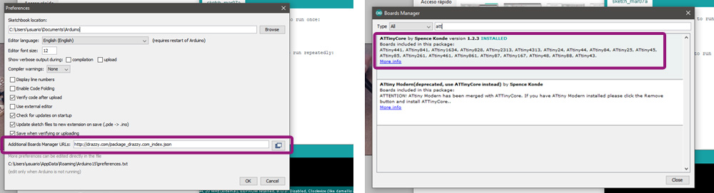
The first thing that I did was to download Arduino IDE. Then I loaded the Board Manager ATTinyCore by Spencer Konde. To do that, in Arduino IDE, I went to file > preferences and in section Additional Boards Manager URLs I copied this URL: http://drazzy.com/package_drazzy.com_index.json. Once this was done I went to tools > board > board manager. In the browser I typed "attiny", I looked for the ATTinyCore by Spencer Konde library and I installed.
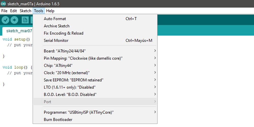
To apply all the changes and new information I closed Arduino IDE and I opened it again. Then, from the tools tab, I chose the version of my PCB board, chip, and clock, as well as the type of programmer.
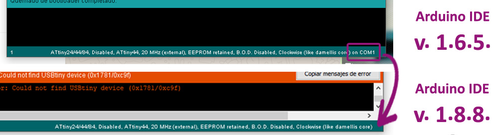
The next step would be to connect the FabISP and the Hello BOARD each other and to the computer and run the burn bootloader command from the tools bar. But I had two problems here:
nº1.- I was using Arduino IDE v. 1.8.8. and for some reason it wasn't reading the port of my computer, so I couldn't send any información. So I uninstalled that version and I installed the version 1.6.5 and then it worked.
nº2.- I thought that, if I connect in the correct direcion all the cords, the LED of my Fab ISP should shine. But I connected everything good and the LED doesn't shine at all!! That got me crazy! The only way for the LED to shine was to connect the FTDI cord upside down and the connector of the flat cord in a very weird position. Look at the image. It is insane! And as you can imagine, I couldn't run the burn bootloader.
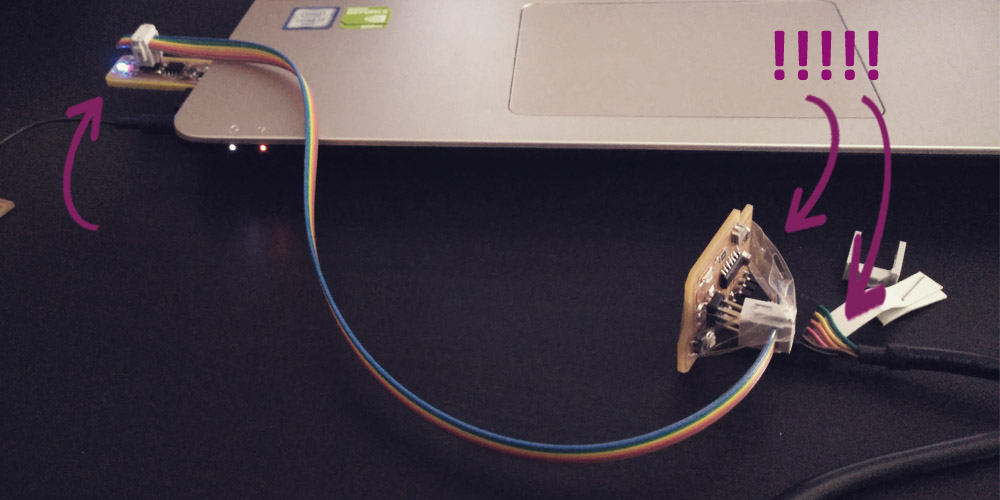
I ckeked all the connections with the multimeter and everything was fine and I even made a new flat cord, just in case. But nothing worked. But then I thought: ¿does the LED do have to shine? So I went back, I conected all the cords in the correct way, keepeng in mind where the ground is, and without caring about the LED, I run burn bootloader and it worked!!
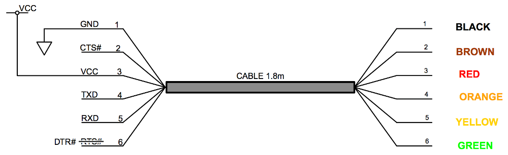
To know where is the ground in my FTDI cord I used this image: Cable ftdi pinout
Then, I uploaded a very basic program from Arduino to check that the board works:
To know for Arduino in which pin is the led and button in my Hello Board I used this image: ATtiny 24/44/84 pinout
Extra. New web design
This week I also uploaded the new design for my web site. I downloaded a template from html5up and I redesigned and reorganized it a bit until I liked enought to start including the information. I took about 3 days to move all the information (six weeks + about + final proyect).
When everyting was ready I followed the bellow steps to uptoad the new version of the web to the online repository:
1. I emptied my local repository. I just erased all the files I had in the master folder. Then I uploaded the emptied repository to GitLab.
2. Then I copied and pasted all the files for the new web to the master folder in my local repository and I uploaded to GitLab again.
3. In GitLab, in the online repository, I added a new file in the master folder. For the template, I chose the .yml file and then HTML (because my web is developed in .html). And I committed the changes. And that's it!
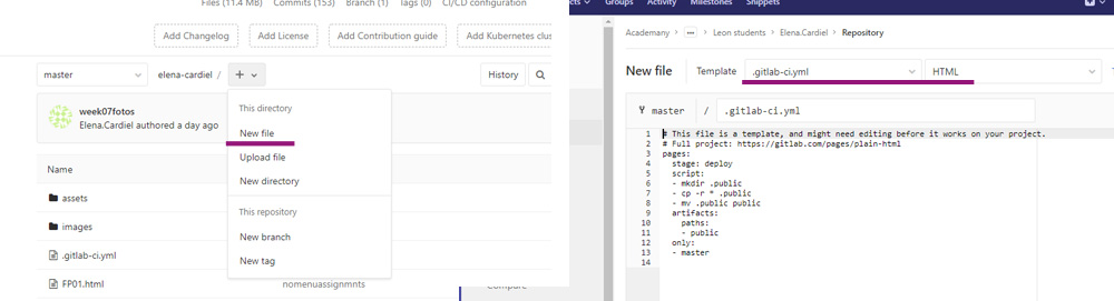
I just had to wait 5-10 minutes (I guess to give time to the system to read all the new information), and the web was completely uploaded!!.
Files
Find below the files that I made for this assignment. Please do not hesitate to download it!! I hope you enjoy it!!
Outline hello-board week07 - .png
Traces hello-board week07 - .png
Eagle (.epf + .brd + .sch) Hello-board week07 - .zip