final project -- weekly assignments -- about me -- fab academy
Week 03: Electronics production
This week's assignment was to build a fabISP, a programmer for Atmel's 8 bit microcontrollers. It's based on the USBtiny project and supposed to be made in a fablab, so it should be done without all the fancy stuff like soldermask, through-hole plating and so on. Ideally, it should be a one-sided board that you can hand-solder. Well, that is a step down from what I normally do for a living, so I'll take it as a challenge. It's not a bad thing to sometimes do something using different limitations than you're used to.
Also, it's a great opportunity: While normally, I use Target 3001!, I have wanted to try KiCad for quite some time now (since the release of version 4, to be precise), so this will be the opportunity to do that - and generate the bug reports I promised one of the devs. Daniel wanted to try KiCad, too, so we mostly worked together on this assignment, helping each other when needed.
2018 Update: A lot has changed since writing that paragraph above. I'm now using Circuit Studio at work, and mostly KiCad for hobby projects. The PCB mill we used in 2016 is (for a number of reasons) no longer easily accessible, and I've grown more than a bit tired of investing a ton of work into designing a PCB to be millable, milling it and then dealing with corroding rivets when I can have way better and nicer results by having them made in china. Milling a PCB is cool to learn, and it's great if you need one really fast (as in: In a few hours), and that's about it. I'm not religious enough to do that just for the sake of being more "fabby".
Phase 0: Coming up with a PCB layout
While I could have just used one of the provided designs, milled it and stuffed it that wouldn't have been half the fun. So, onwards to testing KiCad. It's an interesting project that has been around for ages, and after some "down time" now seems to be under active development. So given that there are no real alternatives that run fine on my Mac, it was an interesting experiment to try it out.
Basic Workflow
In general, PCB creation works in a similar way to most other EDA software:
- Have a great idea
- Work out the schematic of your project
- From that schematic, generate a circuit board layout
- While doing that, find errors in the schematic, return to 2
- Generate production files from the layout
- After making multiple boards, find an error in the layout. Return to 3
Each step is done in its own programme, so you when weeding out design errors, you will change windows quite a bit. Also, you will end up with a bunch of different files for each step instead of the one project file some other software does.
Schematics
While schematics, netlists and layouts are handled by KiCad in different files, any work you do has to be done in a project. A project has its own project file (think of it as the duct tape and zip ties keeping stuff together) and should be put in its own directory to reduce overall clutter problems.
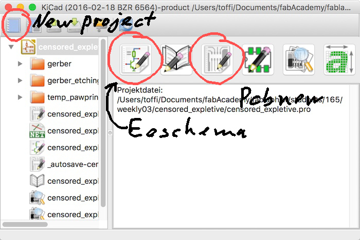
The KiCad project window. Here, a project (my programmer) is already opened. If you need a new one, you can generate it here. All you have to come up with is a name (my spontaneous comment at having to do an AVR programmer was censored by a higher authority) and a place to save the project files. Next, we fire up Eeschema, the schematic editor, to create a schematic of our project. While this is normally a huge part of any electronics project, in our case it's relatively simple, given that we just have to copy a known schematic.
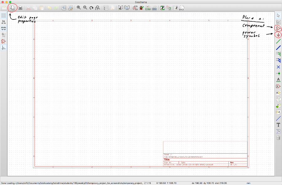
Eeschema handles schematics on pages, and you can print those pages if needed. To do that properly, you can edit the properties of every page according to your needs. There is an intricate system of hierarchical schematics, using one whole schematic one or even more times in a higher level schematic like it was a component. I haven't tried that yet, though, and for something as simple as the USBtiny we won't need it.
To place our first component on the schematic, either activate the "add component" tool and click somewhere into the schematic or press a (you don't have to click then). Both ways will lead you to the component selection window. As a side note: Every tool in KiCad is selected, then activated by the icons in the sidebars. The shortcuts directly activate the tool they are used for. The most brutal difference this makes is with the wire tool, which starts a hew wire at the position of your mouse pointer when activated by shortcuts.
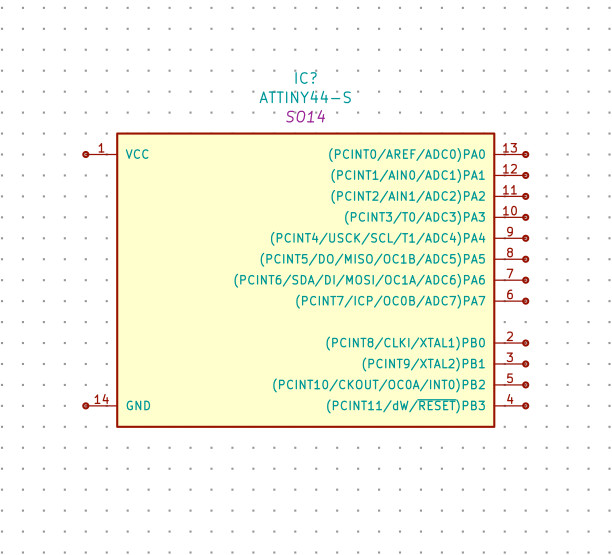
The component selection window lets you choose a component to place, either by browsing through the database or by using the search function. Most more generic components like resistors, diodes etc. are handled just as generic - There is only one symbol for them, and all that extra information like the exact part designation is entered into the component properties afterwards. This does have its advantages, but also its disadvantages - You can't really use it if you want to use a specific inventory of parts and have automatically generated BOMs with order numbers or other information. It does make coming up with a general idea of a schematic a lot faster, though. More specific components like microcontrollers can have a footprint or a range of footprints pre selected, like the one showing up in purple on the screenshot above.
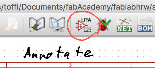
At this point, components don't have a reference "name" yet, just the prefix. The numbering can be done automatically by the annotation-tool or, if you want specific numbers, you can just edit the "reference" field of the part by hand. It doesn't really matter when you do that, as you don't need the components numbered before generating a netlist to push at the layout editor.
Parts selection
Our lab doesn't "just have" the falblab inventory, and buying stuff here at the university is tedious and time consuming, so we had to come up with stuff we could get ourselves... and get it in time. That way, I ended up with some parts not in the standard inventory (like the crystal). Those should be easy to replace if needed, though. Most of the passives are 0603 to make them easier to solder by hand. I forgot ordering the 18pF for the crystal, so I had to use the 0402 that were available.
- IC1: Atmel ATtiny44A-SU, Farnell No. 1699397
- Y1: TXC 7A-12.000MAAJ-T, Farnell No. 1841940
- D1, D2: Orange 0603 LED from our lab inventory
- D3, D4: Diodes Inc. BZT52C3V3-7-F, Farnell No. 1843704
- C1: Murata 0603 10µF capacitor, Farnell No. 2456110
- C2: 0603 100nF capacitor from our lab inventory
- C3, C4: Some 0402 18pF capacitors I found at the lab
- R1, R2, R6: Some cheap 0603 1k5 resistor, Farnell No. 9238506
- R3: Some cheap 0603 10k resistor, Farnell No. 2447230
- R4, R5: Cheapest ~50R resistor we found, Farnell No. 1170657
- P1: Horizontal 6-pin plug, Würth Elektronik, Farnell No. 2470741
- P2: Micro USB connector Hirose ZX62D-B-5P8 from our lab inventory
Networking: Connecting those components
The pins of components can be connected by two ways: First is by pulling "wires" between them, visibly linking them. Alternatively, they can be placed on the same net, and won't need a directly visible link.
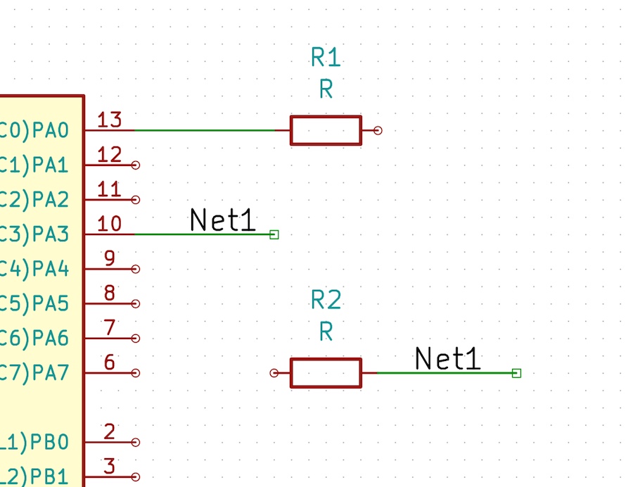
R1 is connected to the controller with a wire - That can be done by selecting the wire-tool or by hovering above the starting point and pressing w. Clicking sets a turning point, clicking on a pin ends the wire. R2 is connected by being on the same net "Net1". To do that, both wires were ended mid-air by double clicking. The resulting nets can be named by right clicking and selecting "Add label" or by hovering on the wire and pressing l. The name itself doesn't matter - It just has to be unique.
Wired can be connected by ending one wire on another one (with a single click) or crossed (without generating a connection). Also, there are additional labels for nets for connections between different levels of hierarchical schematics which we won't need for something simple like the USBtiny.
Intermediate Stuff: Footprints, Netlists
KiCad doesn't exactly keep an inventory of parts you use, as those mainly consist of the schematic symbols and additional info their author put into them (You can add almost anything, as of now that is of limited use, though). Footprints are handled separately and aren't necessarily fixed for a part. The idea behind that way of working is from a time when the mass of components were manufactured to standard pinouts and standard footprints, like any discrete components or logic gate ICs (remember the 74 series...). As it can be problematic if you mainly work with ICs using nonstandard footprints (which are common today) and a lot of work otherwise, KiCad now has the ability to handle footprint pre-selection information in parts. For some, like the ATtiny44, that information is provided by the standard parts library, for others (like "a resistor" or "a diode", it's not. Most of the time, you will end up having to assign at least part of the footprints yourself.
There are two ways to do that. The first, classic one is to run CvPcb when you have finished your schematic. That one works, it feels rather uncomfortable to me, though, as the way I work most of the time means that I have a specific (down to the order number(s) and supplier(s)) part in mind when adding to the schematic.
The second way to do that is to assign the footprint in Eeschema - either by right clicking and then selecting the footprint assignment dialogue or in the "bigger" properties dialogue. In both ways, you'll have to find the right footprint, either by sifting through the libraries or with the search function (which is slow when first invoked, but works).
The data transfer from schematic to layout happens using a netlist, which is essentially a formalized version of your schematic. You have to actually tell KiCad to generate a netlist, which it will just do, then, if it doesn't complain about missing annotations.
PCB Layout Drawing
Pcbnew, KiCad's new layout editor, is being rewritten in important parts. Given that the rewrite is way into the process, but not finished, you have to keep up with a few... oddities. First, there are two rendering modes: Classic and OpenGL. Classic is broken by design in a few details and mostly discontinued, but still the standard setting, as OpenGL, while looking way better and rendering the stack of layers way better, still has its quirks and missing menus.
Classic mode. The layering is particularly broken on OSX, but all tools are where the different manuals suppose they are. Contrary to that...
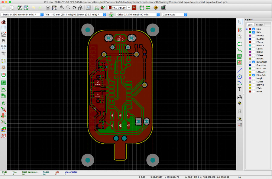
OpenGL mode renders way better, but some of the context menus aren't there yet. If you know them, the keyboard shortcuts will work, though - One example being the redrawing of copper pours, triggered by b.
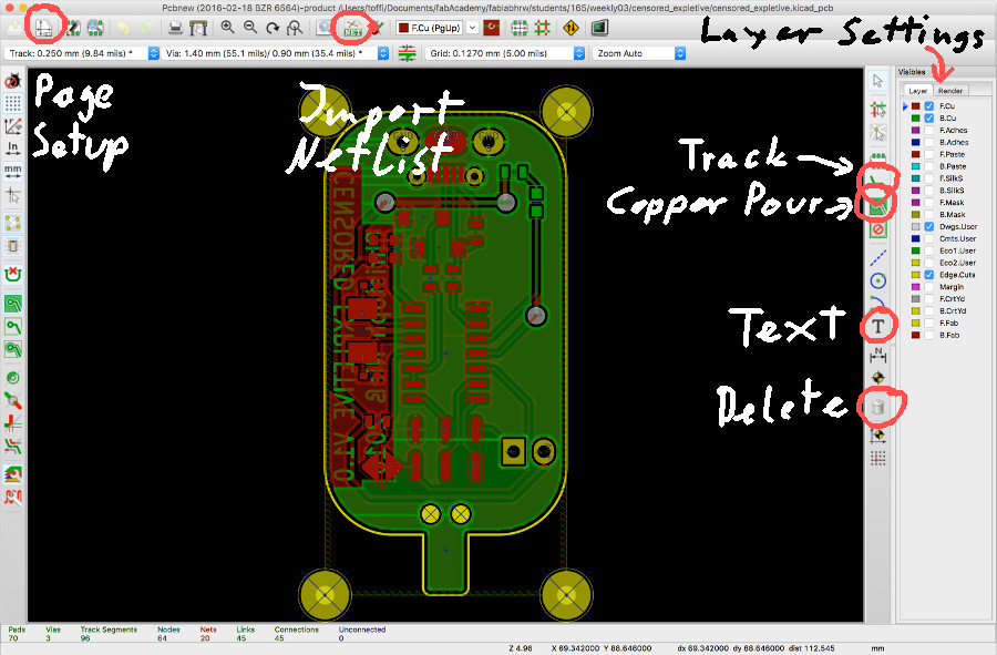
A look at some of the tools we will need to work. In general, the first step of drawing up the layout is to import the netlist generated by Eeschema. You'll have to redo that step every time you make any changes to the schematic to get those changes into Pcbnew. You'll get all the footprints... In exactly the same place. There is a function to somewhat spread them out, though, which you can access by pressing right clicking on them and selecting "global spread out". They will still be around the same place, but spread out enough to individually grab them.
As with components in Eeschema, you can move footprints around by either hovering over one and pressing m or by pulling a marking frame around a bunch of them. Also, you can rotate them by pressing r. Arranging stuff is mostly a matter of experience, but a good starting point is to try and get as few crossings in the white "airlines" KiCad uses to show you the missing connections as possible.
Next, all those virtual connections will have to be made real. It's a lot more comfortable to use OpenGL mode here, as it does have interactive design rule check - It will try to find a way around obstacles, not even allowing you to short out different nets. Classic mode can't do that, and will simply abort making a track if you violate the design rules you set...
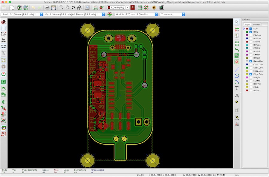
I tried to minimize the use of the backside of the circuit board, given that most people at fablabs seem to have massive problems connecting vias. We do have a simple and not-that-expensive solution here at the lab, so when the problem came up, I did use one bridge on the back side (you could use a piece of wire instead, it's really just one straight bridge, just a bit long to use a 0 Ohm resistor) and placed one of the LEDs there (which you could just leave away, it doesn't have any special function you really need). So, it's still possible to do a one-sided version (with one wire bridge), but if you have the tools to use both sides, you can do that, too. More on the through-hole connections will be documented in the next phase of the build, also, until I do a photo series, Daniel has a nice set of photos of the process.
Fabrication Data
To actually make the board you just fucked up designed you need to output the board layout in some form you can use to make it real. For most processes, that is either gerber or something like pdf, maybe just a printpout to expose and etch boards. Our mill needs gerbers, so that is what I made. The function to do that is available via File -> Plot and can be configured to the needs of whatever you want to feed the files into. Other output options include svg, so it's no problem to feed a KiCad design into the fabmodules, either.
The whole KiCad-project including fabrication data is of course available here.
final project -- weekly assignments -- about me -- fab academy
