final project -- weekly assignments -- about me -- fab academy
Week 03: Electronics production
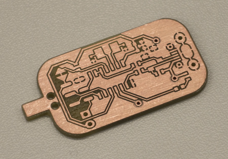
Phase 1: Making the PCB
Using Our PCB Mill
We do not have a "normal" CNC mill at our lab, so using one to do the boards was out. We could have gone to our partner lab at Kamp Lintfort and done it there. We didn't, though. Also, I could have etched the board, which we do have the equipment for. We do, however, also have a CNC mill that is purpose-built for the job, so I used that one.
The process itself is more or less painless as the software can read gerber files and generate the milling tracks using the tools it has. Also, finding the right position after flipping the PCB to mill the bottom side is simple with the neat camera system. It does have its quirks, though.
First, while the PCB is kept in place and level by a vacuum table and milling depth is kept constant with a mechanical depth adjuster "riding" the PCB, getting it right in the first place is a bit of work even with the "automatic system". Also, the attached software "Circuit Pro" is way better than the older version I know from Krefeld, but it's still a mess in some places.
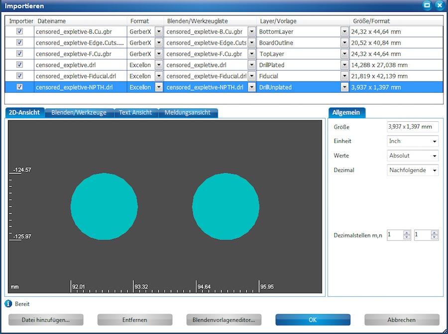
The general work flow is simple: Make a new project in Circuit Pro, with one or two "sides" as needed. Load the gerber files generated from your CAD solution of choice and assign them to the layers Circuit Pro uses:
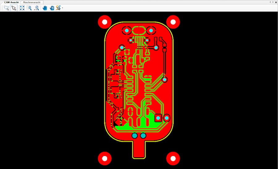
The result should look familiar, as it should look like the board you came up with:
At this point, you have a choice of work flow. The mill needs a set of (at least three) fiducials. Those are markings (holes drilled into the board in most cases) that are used to "find" your layout on the working area when the board position might have changed - like, after doing galvanic through hole plating or after flipping the board to mill the bottom side. You can add those in your CAD package and export them to their own gerber/excellon file, or you can add them in Circuit Pro. If you want to do them in your own CAD, they have to be drilled holes of 1.5mm diameter. Also, they must not be part of the normal set of holes to drill. In the screenshot above, they were done before inporting into CircuitPro - the four holes at the corners of the layout, marked in white instead of light blue.
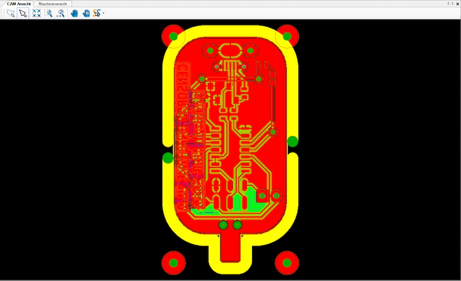
Hit "generate milling tracks", don't forget to set the copper thickness to a sensible value (a bit more than the "official" copper plating of your boards), set the rubout mode to a sensible option (either "partial rubout" or "full rubout", most of the time "full rubout" will be more sensible) and let the path generator run its course.
As a side note, you could, in theory, also produce the milling tracks externally and import them into their respective layers in Circuit Pro. I haven't tried that yet, though, and at the moment I see no reason to do it.
Change to the "machining" view and start the sequential running of all machining steps. The software will guide you through the steps to get your board, which don't require much on your part now if everything was set up correctly. You'll have to put a piece of circuit board into the machine, tell the software where to place your layout (you can manually move the milling head to check) and then tell it to go for it.
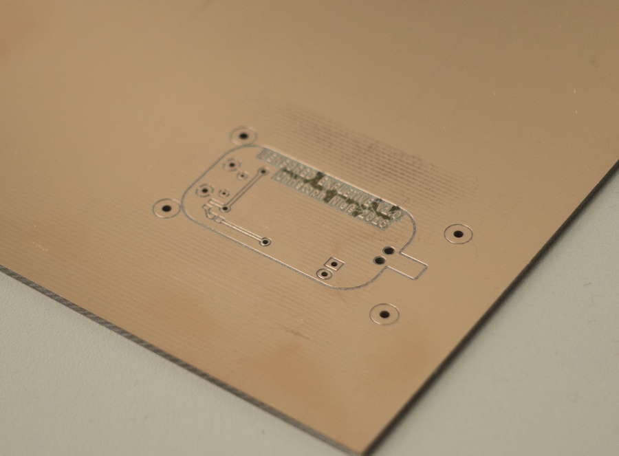 Next you'll hear is the software telling you to flip the circuit board and check on the camera autofocus for finding the fiducials. It's worth taking some time in this step, as the whole process is still a little touchy. Again, next you'll hear from the machine is when it's done.
Other Ways To Do It
Milling will only get you so far - clearing out large areas is somewhat problematic, on the other hand getting really fine structures is hard (and expensive, those mills wear down quickly!). So, as we are allowed to have it and use it, we do have equipment to etch circuit boards at the lab. We also have a cheap inkjet photo printer that prints great "films" for exposing stuff onto the boards. As a test, I wanted to etch one board and etch fiducials into the copper layer, then have the PCB mill drill it and mill the outside contour.
I didn't get around to doing that as our etching tank broke (again), so until I fix that I won't be able to etch boards. I still want to make a new one from laser-cut acrylic, so I might just do that instead. In any case, it will take some time until I can do my experiment as priority is too low to do any repairs now. I will get back here and write about it when I get around to doing it, though.
Another way to make the board would have been to cut the copper traces from copper foil using the vinyl cutter. I want to try that at some point, we don't have copper foil yet, though, so I can't. It's a really interesting concept as it allows for cheap multilayer production. Connecting Vias will be an interesting problem, though.
Connecting Vias With Rivets
One way to connect Vias is to solder a small piece of wire through the hole. The pin of a through-hole part works fine, too, but I don't really like those as they're huge. The PCB industry does galvanic plating through the holes, requiring a huge amount of chemicals that are not only hard to handle but seriously dangerous. We won't do that at the moment, there are interesting approaches I want to test at some point in the future, though.
What we do have at the lab is a via connecting set made by Bungard. It works by riveting copper rivets into the holes, a somewhat time-consuming but surprisingly easy process. Previous work with those has shown that for high current connections (a few amps continuous current) it's better to solder the rivets to both sides of the board, too, but for any normal stuff it's completely unnecessary. Protecting the board from corrosion gets more important with the rivets, though, as the copper below a rivet's head can crumble to dust, leaving a perfectly looking, but completely unconnected via.
I did spray the board with protective, but solderable PCB varnish after that to protect it from fingerprints and general crumbling.
Phase 2: Burning Your Fingers Soldering...
Normally, I would have done this (mostly) SMD board with solder paste and out oven. As not everyone seems to have access to those (Why? Both are easy to get?), we were supposed to solder the assignment by hand, which is of course possible. So, I soldered this board by hand.
I won't do a soldering tutorial here, there are plenty of good (and bad) ones out there already. SMD soldering is no different, mostly it's just smaller and harder to reach, so a microscope is a great help. In some cases (like the micro USB connector on my board, propping the board up so you can see below parts is essential, too. Masking tape is a great help and resolves the problem of humans only having the insufficient amount of two hands.
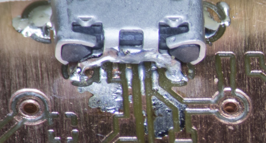
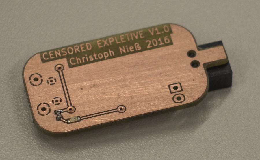
Note the areas of tinned ground plane around the connector - The varnish I used acts like flux when it's not been on the PCB for too long, so any touching with the soldering iron will immediately lead to a tinned blotch. Also, note the rivets in both vias.
Here, all used pins of the connector are soldered to the board, there are no visible bridges, so everything's fine. The somewhat matte finish of the joints is normal with our lead-free solder (While we are, contrary to Neil, allowed to have etching stuff at the lab, we are absolutely forbidden from having lead solder wire...).
Next, I soldered the ATtiny, starting with one tinned pad, placing the IC with its leg into the hot and molten solder on that pad. It is fixed in place by that so you can solder the other pins painlessly, but that first pin might need some rework with a little flux afterwards. After the ATtiny, I continued outwards - I placed the components tightly enough that you won't be able to reach the more central ones with a soldering iron after the outer ones are in place, that takes a bit of planning. Also, I wouldn't have been able to reach the half-hidden pins of the USB connector after soldering the zener diodes next to it:
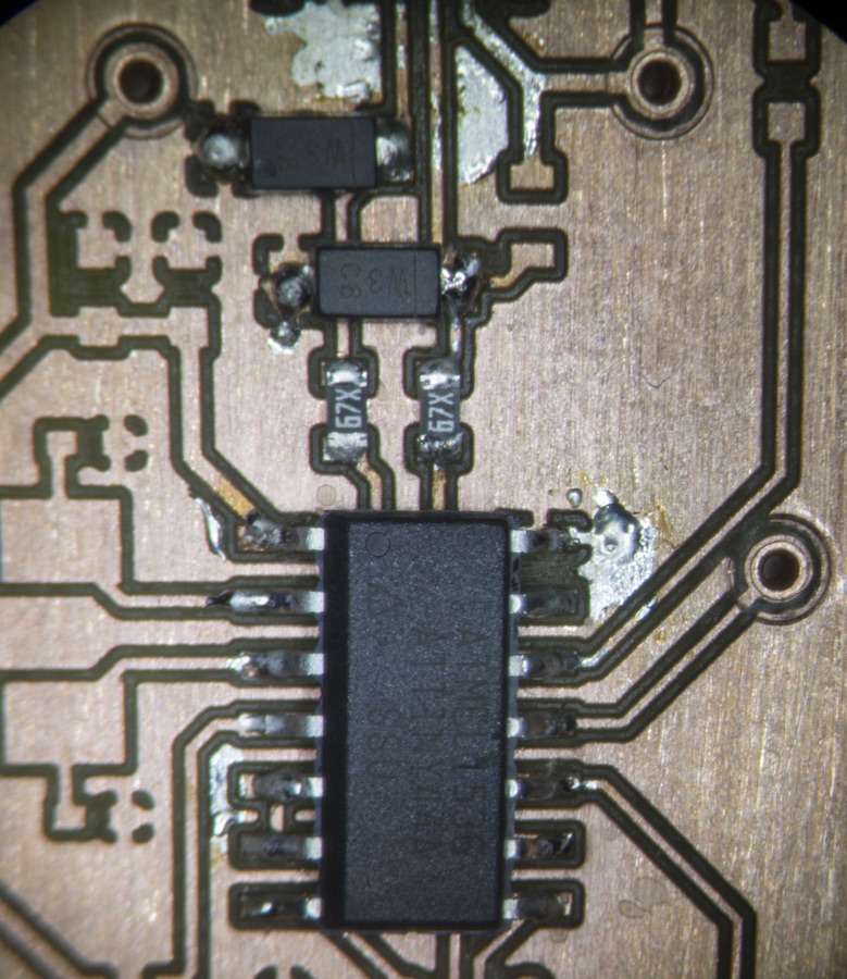
Note the pre-closed solder jumper next to the ICP plug. It was an experiment, as in theory, I would only have to have it closed once (for flashing) and never again. Had that assumption been true it would have worked beautifully, so it might be a footprint worth keeping.
The crystal we had is a bit ugly to solder as its pads are almost unreachable from the sides of the package, but it worked out. Also, the LEDs are rather sensitive as their clear housing tends to melt. Also, that ICP plug is a pain to solder in as the bottom middle pin is almost unreachable.
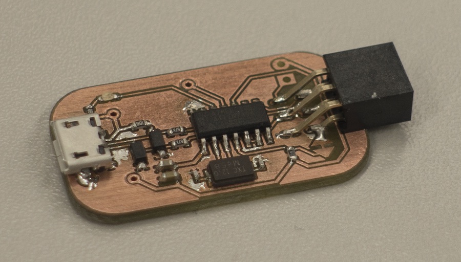
Only the pin header for the jumper left to solder in, which is easy as it's a horizontal one. At that point, I taped the board down upside down and added the bottom side LED and its resistor:
final project -- weekly assignments -- about me -- fab academy
