Week 13
Networking and Communications
The theme of this week was "Networks and communications", which helped me to learn about various communication protocols, such as Serial bus, I2C, SPI, etc.
The objective of this assignment were:
The objective of this assignment were:
- Design and build a wired &/or wireless network connecting at least two processors
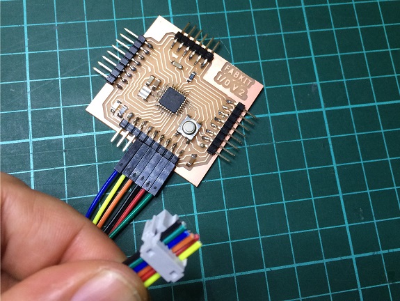
For this assignment, I decided to use the I2C protocol, I previously made a two PCB Fabduino FABKIT 2.0 that I connected one to the another.
In the I2C protocol, two controllers (fabduino) communicate by sending signals through a medium, in this case a Ribbon cable. The transmission is from the slave to the master through the pins of the processor. I chose to send the signal by pin 8.
In the I2C protocol, two controllers (fabduino) communicate by sending signals through a medium, in this case a Ribbon cable. The transmission is from the slave to the master through the pins of the processor. I chose to send the signal by pin 8.
My Workplan
1. Design, mill, weld and program a FabDuino..
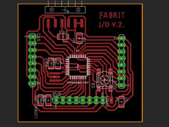
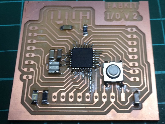
As I said lines above, I used the FabKit v2, I used the same distribution of the elements but I re-drew it in Eagle to realign the tracks, because I did not have the 1/32 cutter bit, instead I had a 1/16 milling bit and if I cut it with the original design I would lose several tracks. In this design, the cutting border should be more separated from the tracks.
For the use of the Eagle design tool, I followed the steps that in my assignment of week 6 "Design of Electronics", you can see here.
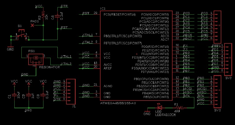
As you can see in the schematic design, the microprocessor used is ATMega48 / 88/168-AU and it is in the FAB library it is compatible with the ATMega 328 which is the processor that I will use in both boards.
As you can see in the schematic design, the microprocessor used is ATMega48 / 88/168-AU and it is in the FAB library it is compatible with the ATMega 328 which is the processor that I will use in both boards.
This is the board with all the components aligned and the tracks re-arranged.
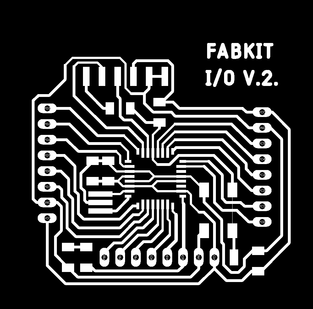
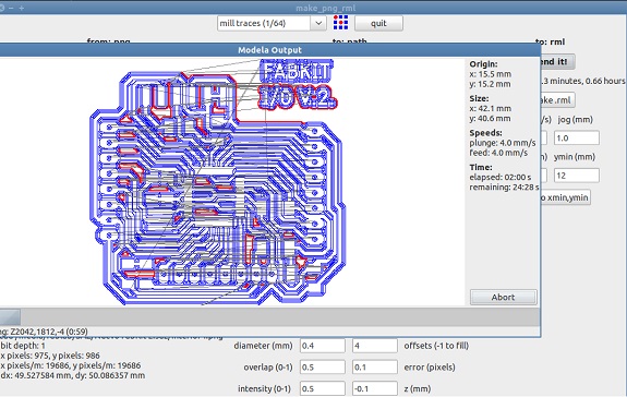
These are the PNG files that I used to mill the PCBs
Files to download
Fabkit schematic
Fabkit board
Cutter
Board
Files to download
Fabkit schematic
Fabkit board
Cutter
Board
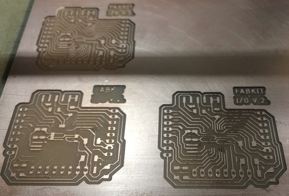
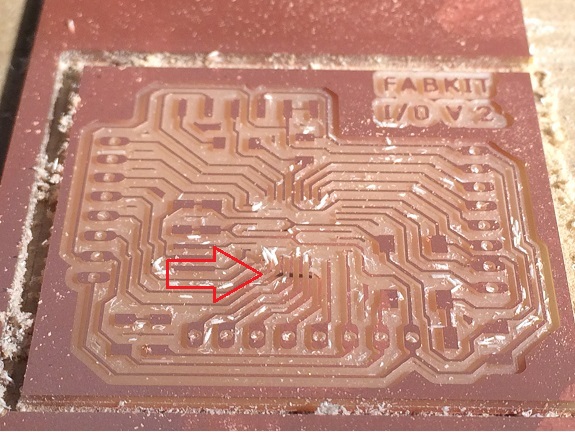
For the milling process of tracks I used the 1/64" milling bit and it took about 26 minutes.
Here you can see a couple of videos from part of the milling process of the PCB tracks with the 1/64" milling bit and the contour cut with the milling bit 1/16" (at that time there was no 1/32").
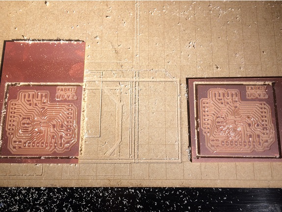
Problems during the milling process
Although I had already milled several PCBs before without major problems, this time it cost me several attempts, in most the problem was that the tracks were broken and got up, I could modify the design to make the tracks to 16mil, but even so the tracks were up.
Finally I could mill a couple of PCBs with the least number of faults, in both there is a track that passes between the Pads of the side connectors that is attached to one of them and in the other two tracks that go to the microprocessor were broken and lifted .
Solution
Solution
- I used a cutter to separate the track from the Pad and in the case of the tracks that go to the processor,
- With a tweezers I straightened them taking care not to break it and welded the processor on top
- Finally, in the case of the missing track, I soldered a piece of copper wire 0.3 mm from the track to the pad of the micro processor.
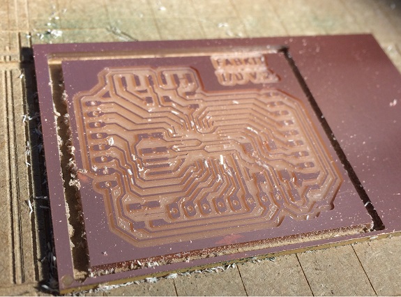
This is an approach to one of the PCBs, you can see in the center the tracks that go towards the micro processor raised towards the camera.
Bill of materials
- 2 ATMega 328 SMD microprocessor,
- 2 Resistor 499 Ω
- 2 Resistor 10 KΩ
- 2 Led SMD
- 2 Switch push button SMD
- 2 Resonator 20MHz
- 2 Capacitor 10 µF
- 2 Capacitor 1 µF
- 4 Capacitor 0.1 µF
- 4 Pin male
Welding the components
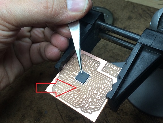
In this image, I am placing the microprocessor on the PCB, you can see the missing track.
Once secured the tracks with the microprocessor on them proceeded to weld.
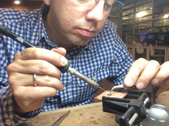
I welded all the components following the guidelines as in the assignment of week 6 "Electronics design"
In this picture you can see how I fixed the track that goes to pin 16 with a copper wire covered with tin.
In this picture you can see how I fixed the track that goes to pin 16 with a copper wire covered with tin.
The ATMega328 microprocessor
This is the ATMega328 microprocessor pinout, it includes the pin numbering for Arduino..
Datasheet ATmel328
Datasheet ATmel328
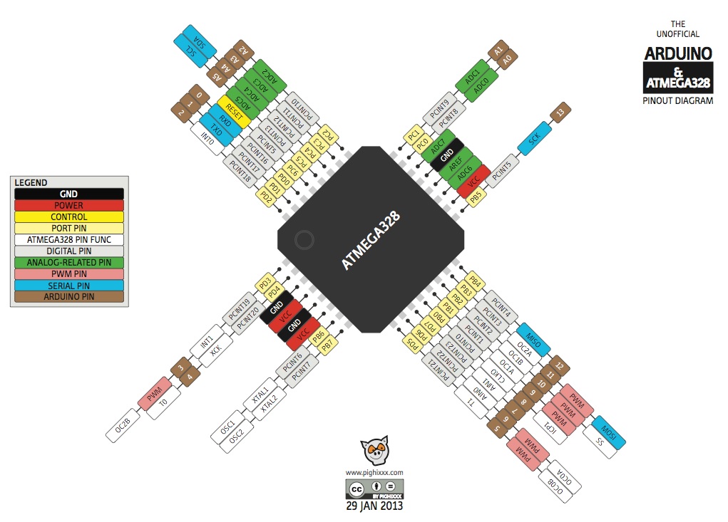
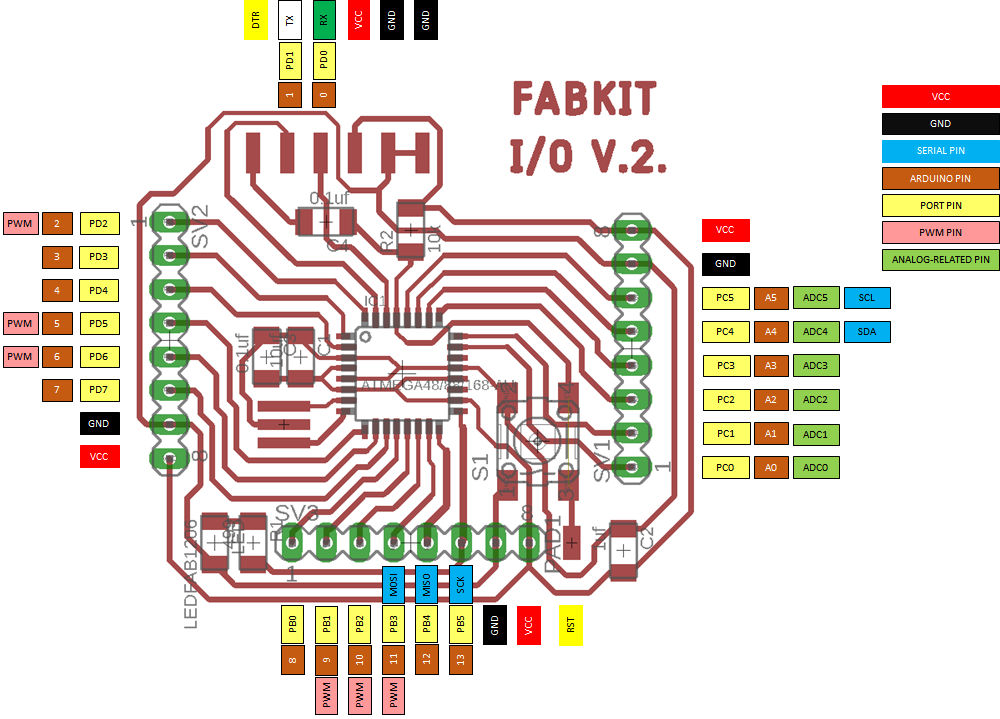
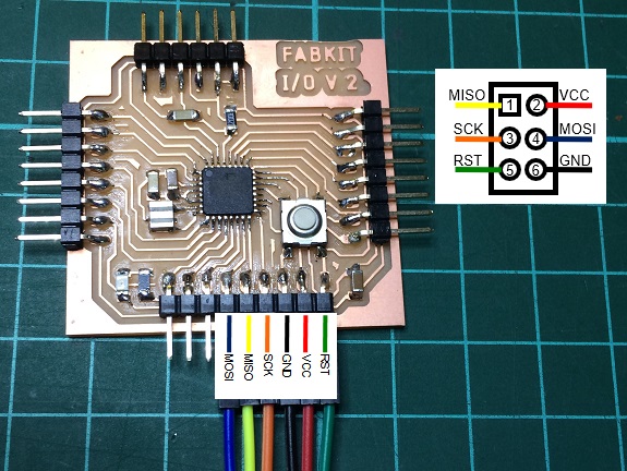
Based on the previous pinout of the AtMega328 microprocessor, I prepared this pinout of FabKit V2.0. I found it very useful to organize myself and not make wiring mistakes.
For zoom, click here
For zoom, click here
Electrical Characteristics
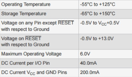
Before using any kind of chipset, we must read the electrical characteristics section on its datasheet, so that we can avoid that the chipset get burned accidentally.
Some basic parameters we must look for in a datasheet are the maximum and minimum power source voltage, the maximum curent that can be obtained from its output pins and the maximum current that the chipset can give summing the current from all its output pins. If one of this limits values is exceeded on the chipset, it will get burned.
On the Atmega 328p this parameters are specified in Absolute Maximum Ratings and its corresponding values are 6V, 40mA and 200mA respectively.
Comunication:
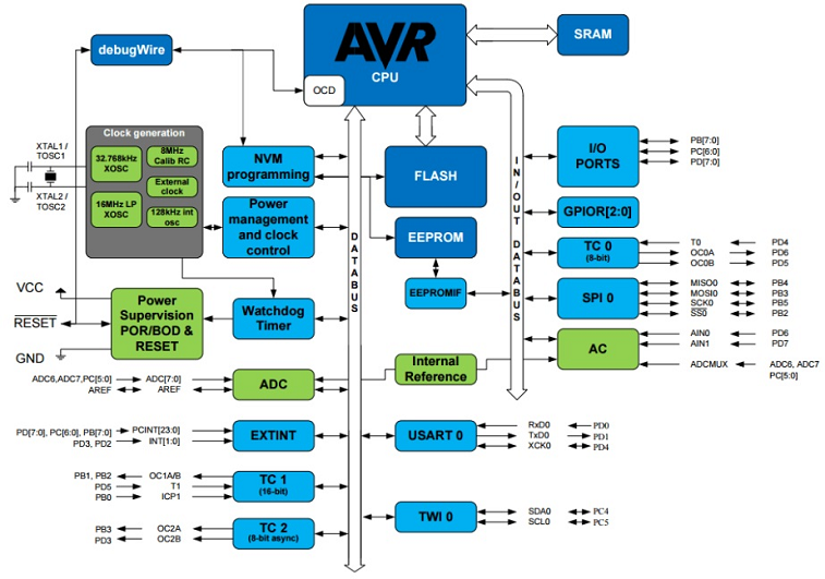
The Atmega 328p can communicate with other devices by serial communication (this means that the data is transmitted in a serial way by its comuncation interfaces). This Microontroller has an internal USART, which is a piece of hardawre wich can comunicate by sending TTL signals, and it also counts with internal SPI and TWI modules which permit it to comunicate in SPI and I2C protocol respectively.
The Atmega 328p can communicate with other devices by serial communication (this means that the data is transmitted in a serial way by its comuncation interfaces). This Microontroller has an internal USART, which is a piece of hardawre wich can comunicate by sending TTL signals, and it also counts with internal SPI and TWI modules which permit it to comunicate in SPI and I2C protocol respectively.
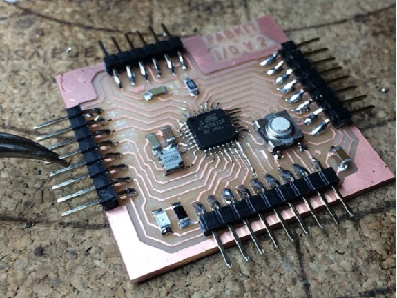
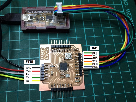
Identifying and preparing connections to ISP and FTDI
I used the schematic diagram to identify the pins that correspond to the ISP port The pins for the ISP connection are at the bottom of the next image.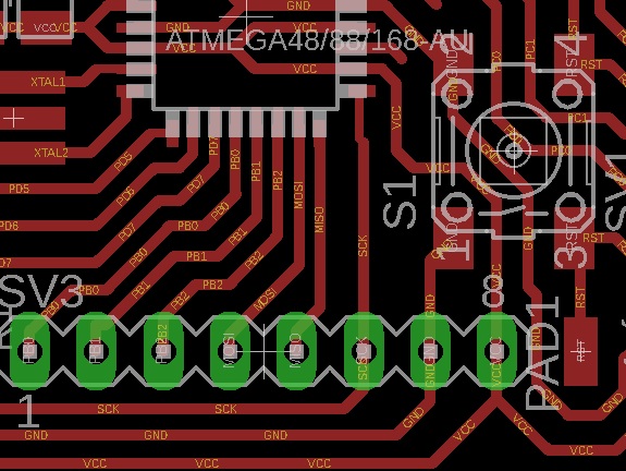
Then, I prepared the ISP 2x3 header, according to the scheme shown above.
Burning the Bootloader
Before I started programming the Fabkits, I had to burn the ATMega328 Bootloader. The Bootloader is a small piece of code (generally 512 bytes) located at the end of the address space in the microprocessor's Flash memory and can not be programmed as a normal sketch. The Bootloader is executed when restarting the microcontroller and its task is to verify if a new sketch has been sent from the Serial / USB port, if so, it will be saved in Flash memory, otherwise it will execute the sketch that is already.
Source: https://www.arduino.cc/en/pmwiki.php?n=Tutorial/ArduinoISP
Error burning the bootloader
My first attempt to burn the bootloader was not successful.
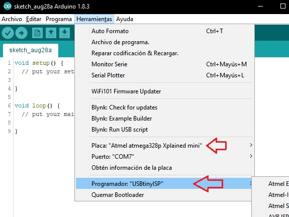
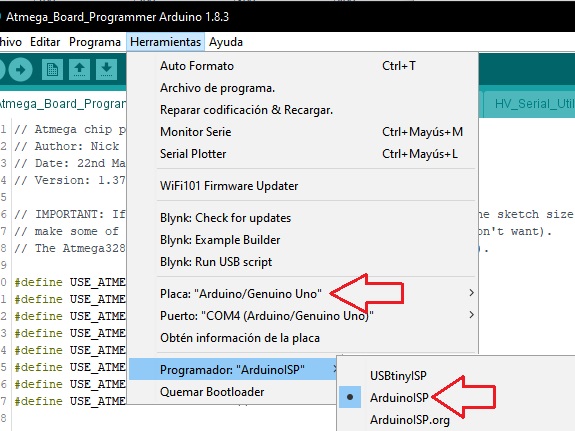
As I showed in other images, I connected my FabISP to the ISP pins of the Fabkit and the USB-FTDI cable to the FTDI pins. Then in the IDE of Arduino I selected the Fabkit board as "Atmel atmega328p Xplained mini", and my programmer as "USBtinyISP", then I ran the option "Burn bootloader" from the tools menu.
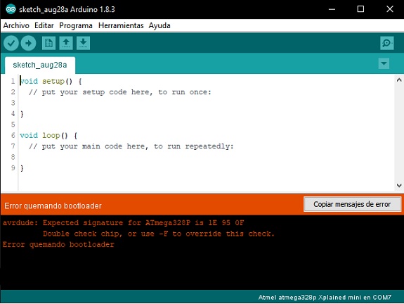
The result was an error message, the burner does not recognize the signature of the atmega328P.
My first attempt to burn the bootloader was not successful.
As I showed in other images, I connected my FabISP to the ISP pins of the Fabkit and the USB-FTDI cable to the FTDI pins. Then in the IDE of Arduino I selected the Fabkit board as "Atmel atmega328p Xplained mini", and my programmer as "USBtinyISP", then I ran the option "Burn bootloader" from the tools menu.
The result was an error message, the burner does not recognize the signature of the atmega328P.
From what I read in other forums, the Atmega328P-AU microprocessors have a different signature than the Atmega328P installed on the Arduino boards. I also read that changing the signature in the avrdude.conf file could overcome the error message, but it did not work.
Error with ArduinoISP
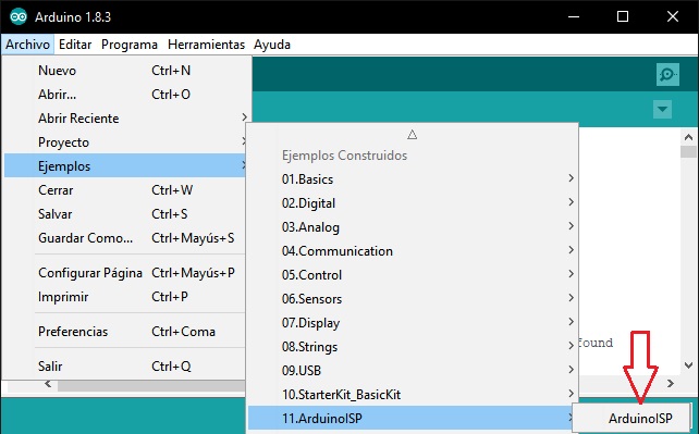
I followed the steps indicated on the page Arduino as ISP and Arduino Bootloaders .
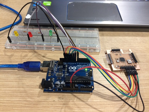
I downloaded the ArduinoISP sketch, I connected the pins pins 11, 12, 13 and 10 of the Arduino board connected to MOSI (blue), MISO (yellow), SCK (orange) and RESET (green) respectively, also the LEDs and resistors as indicated in the instructions.
I followed the steps indicated on the page Arduino as ISP and Arduino Bootloaders .
I downloaded the ArduinoISP sketch, I connected the pins pins 11, 12, 13 and 10 of the Arduino board connected to MOSI (blue), MISO (yellow), SCK (orange) and RESET (green) respectively, also the LEDs and resistors as indicated in the instructions.
Then, I selected the Arduino board and ArduinoISP as a programmer, to record the sketch on the Arduino.
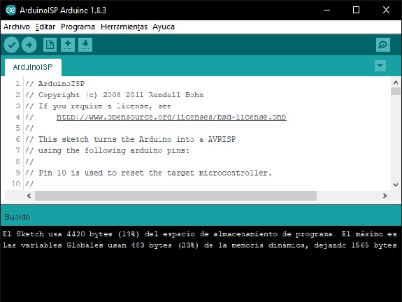
Up to this point, there were no problems, the ArduinoISP sketch was loaded onto the Arduino board that I would use as a programmer.
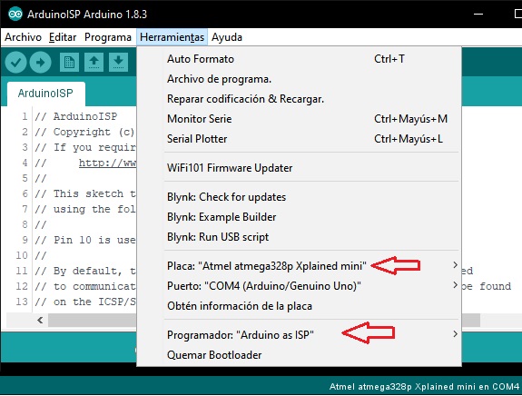
The next step was to connect the Fabkit by means of the ISP cables to the Arduino and change the definition of the board and the programmer by Atmel Atmega328p and "Arduino as ISP".
The next step was to connect the Fabkit by means of the ISP cables to the Arduino and change the definition of the board and the programmer by Atmel Atmega328p and "Arduino as ISP".
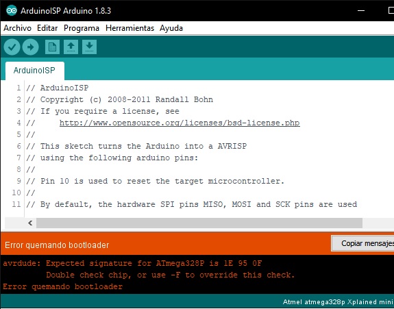
Finally, burn the bootloader. But again I got an error message similar to the other method.
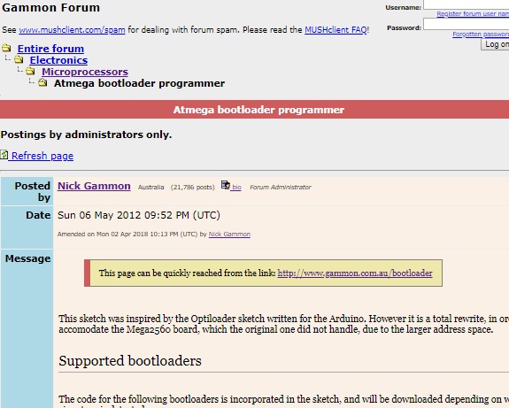
I kept looking for information on how to burn an ATMega328p-AU microcontroller and found a forum that recommended this page:
http://www.gammon.com.au/forum/?id=11635
The page explains the operation of sketches to load on the Arduino board and to obtain information about the signature of the processor connected to this board and finally burn the bootloader.
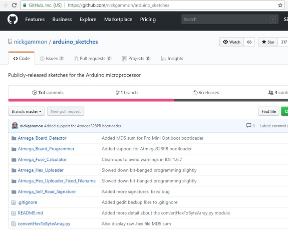
On that page there is a link to GitHub with the sketches to use.
https://github.com/nickgammon/arduino_sketches
The page explains the operation of sketches to load on the Arduino board and to obtain information about the signature of the processor connected to this board and finally burn the bootloader.
On that page there is a link to GitHub with the sketches to use.
https://github.com/nickgammon/arduino_sketches
I downloaded the files and loaded the sketch "Atmega_Board_programmer.ino"
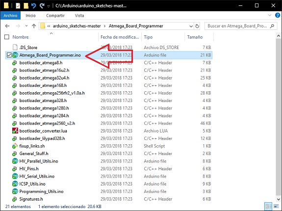
As in the previous method, the sketch is loaded on the Arduino board like any other sketch.
The difference is that from the Serial monitor the whole process of burning the bootloader is managed.
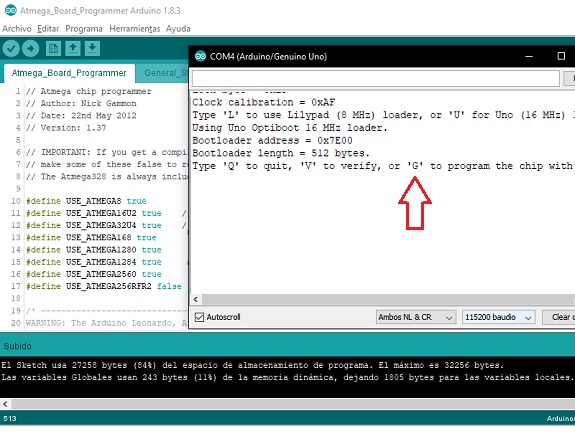
In the following image the Arduino board connects to the Atmega328 microprocessor and extracts information, then waits for the resonator frequency to be selected, in my case, as I used a 20MHz resonator I selected the "U" option.
In the following image the Arduino board connects to the Atmega328 microprocessor and extracts information, then waits for the resonator frequency to be selected, in my case, as I used a 20MHz resonator I selected the "U" option.
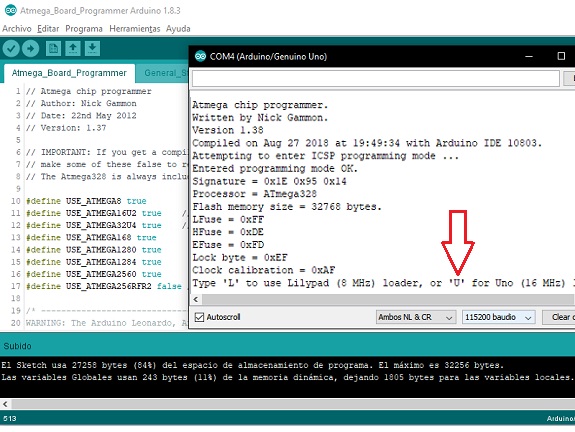
In the following images, you can see the process of burning the Bootloader.
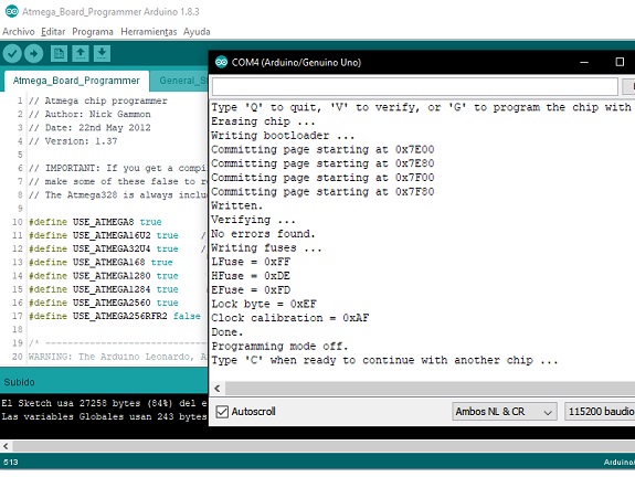
This video shows the process of burning the bootloader from an arduino board.
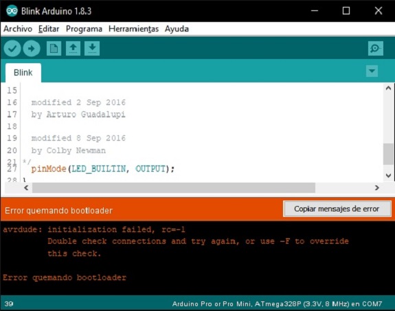
Despite having been able to burn the bootloader with this last method, when connecting the USB / FTDI cable to the Fabkit I could not upload the program, I still get error messages.
Solution !!
I checked the design in Eagle and noticed that the track I had added was not necessary to join points 3 and 4 of the pushbutton switch, since these points are linked inside the switch. After making this change, I re-ground two PCBs.While the Roland mill worked on my new PCBs, I continued to review documentation on how to overcome the signature error and then I found one of the causes: I used ATMega328, not ATMega328P, this small difference implies a different signature on the microprocessor, which is not recognized for the Arduino IDE.
That is:
- ATMega328 ---> signature: 0x1e 0x95 0x14,
- ATMega328P ---> signature: 0x1e 0x95 0x0F,
- I looked for the file avrdude.conf (it is in: C: \ Program Files (x86) \ Arduino \ hardware \ tools \ avr \ etc),
- I saved a backup (always save a backup),
- I opened it in a text editor,
- I searched: "0x1e 0x95 0x0F" (this is the signature ATmega328P) and I replaced it with: "0x1e 0x95 0x14" (this is the signature ATmega328),
- I saved the file and rebooted Arduino.
By the time I was able to make the changes, I already had two new FabKit with blue LEDs ready (the previous two were green).
For this version I used ATMega328P, I could only burn the bootloader of one of them, the other did not respond with anything.
So I had to do one more fabkit, this one I put red led to keep the account.
So I had to do one more fabkit, this one I put red led to keep the account.
After welding the components of the fifth Fabkit (red LED), I proceeded to check all the welding points, copper tracks raised or broken, ISP and FTDI correct wiring.
This fabkit was recognized and proceeded to burn the bootloader.
As a check I took the "Blink" sketch and I uploaded it to my last Fabkit. Then, as a test, I connected each of the previous fabkits, with the re-soldered contacts and I was able to burn the bootloader with my FabISP and upload the same blink program with the FTDI cable!
Now I have four Fabkits, the first two I could recover them.
2. Connection between the components of the boards.
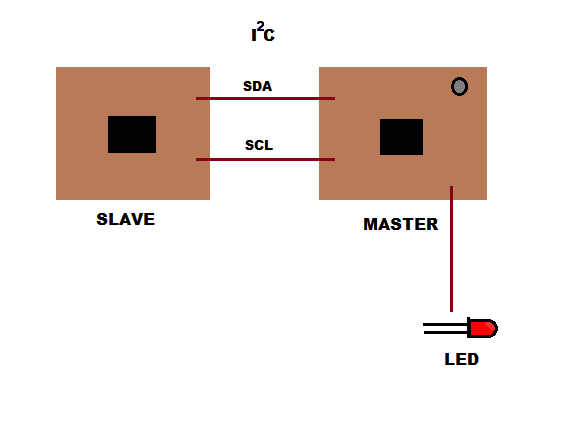
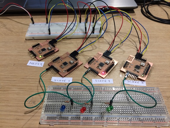
To create an i2C communication all Fabkits must be connected to the SDA and SCL pin between them. They will also share land and Vcc; as in the following figure.
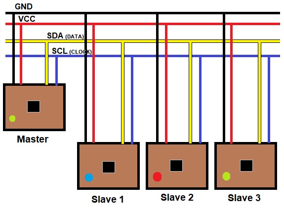
To determine which are the SDA (data) and SCL (clock) pins, I used my schematic diagram. The SDA corresponds to the PC4 pin, and SCL to the PC5 pin.
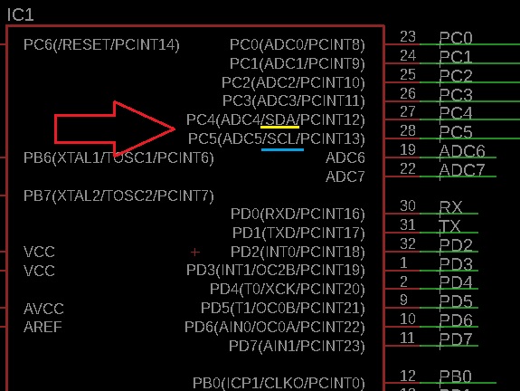
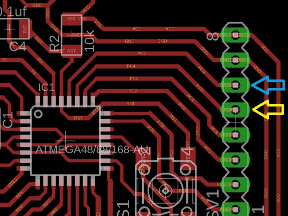
The following image shows the physical location of pins PC4 # 27 and PC5 # 28.
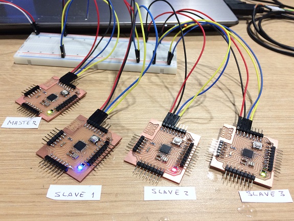
In this image, all the fabkits are wired, I keep the same distribution of colors to avoid confusion.
You can also see the LEDs on, because everyone is independently executing the Blink sketch.
You can also see the LEDs on, because everyone is independently executing the Blink sketch.
My plan was to program the slaves for everyone to blink their LED, and suddenly, the master will select a slave randomly and it will execute an action with the external LED that is connected to the PD3 pin.
The PD3 pin is a digital pin that can work with PWM pulses, emulating an analog signal.
The PD3 pin is a digital pin that can work with PWM pulses, emulating an analog signal.
3. Programming of master and slave boards.
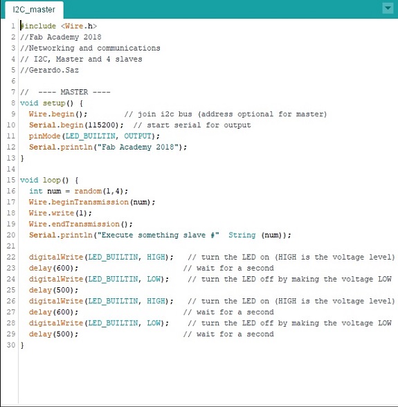
This is the Master's sketch.
In the Setup section: the Wire.begin () command with no parameters is used by ATMega 328 to connect to the i2C bus as Master. In the Loop section: with the commands Wire.beginTransmission (XX) and Wire.endTransmission () they delimit the commands that the XX slave will receive, this transmission is made to the i2C bus and although it is read by all the connected slaves, it will only execute the commands the slave XX.
In the Setup section: the Wire.begin () command with no parameters is used by ATMega 328 to connect to the i2C bus as Master. In the Loop section: with the commands Wire.beginTransmission (XX) and Wire.endTransmission () they delimit the commands that the XX slave will receive, this transmission is made to the i2C bus and although it is read by all the connected slaves, it will only execute the commands the slave XX.
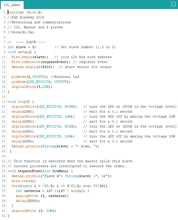
This is the Slave's sketch.
In the Setup section: the Wire.begin (XX) command with parameter is used for the ATMega 328 to connect to the i2C bus as a slave identified with the XX byte.
The Wire.onReceive (requestEvent) command is used to define the function that will be executed when the slave is called by the i2C bus. In the Loop section: I just defined a Blinks process of the internal led (pin # 13) to simulate that the processor is doing something. The requestEvent () function: It is executed interrupting the process of the Loop section, regardless of where it is located and sends PWM pulses to pin 3 that has an external Led connected.
4. Funcionality test.
In the following video, you can see when the Master randomly sends the command to a Slave through the i2C data bus, the slave interrupts the process in which it is doing (internal Blink Led) to attend the Master order (external blink led) , then it continues at the point where its process was interrupted.
Files to download
 I2C_master.ino
I2C_slave.ino
Files to download
I2C_master.inoI2C_slave.ino