Week 7
Electronics Design
Group assignment
Individual assignment
Learning outcomes:
- Select and use software for circuit board design.
- Demonstrate workflows used in circuit board design.
Have you:
- Shown your process using words/images/screenshots.
- Explained problems and how you fixed them, including how you worked with design rules for milling (DRC in EagleCad and KiCad).
- Included original design files (Eagle, KiCad, Inkscape, .cad - whatever).
Click here to go to the programming of the board.
Individual assignment:
1. General circuit knownledge:
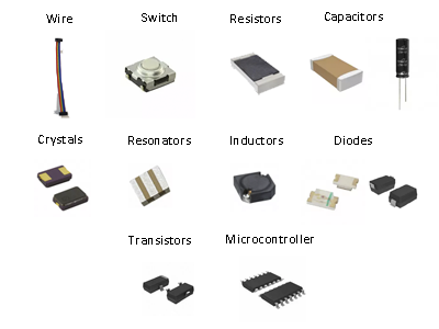
Components:
- Resistor: As the name indicates, resistors have an electric resistance that limits the flow of the electrons through a circuit. Their role is very important in circuit designing, for example, if you connect a battery to a LED directly it will explote, you need to connect a resistor in between, usually a 1KO one. The resistance is measured in ohms Ω. And an important aspect that we have to look at is the tolerance: how accurate it is.
Current(I) = Voltage (V) Resistor (R)Equation 1 - Capacitors: they are also a key component in almost every circuit. They store energy in a electric field and they can control voltage spikes. They can be polarized and unpolarized.
Capacity =Charge (Q) Voltage (V)Equation 2
- Inductor: stores energy also but in a magnetic field.
- Wire: makes electrical connection between programmer and the board.
- Switch: this component allows you to control wether an electric circuit is open or close. They are very important for user interaction.
- Crystal and resonators: they provide a clock signal to the circuit.
- Diodes: their main function is to control the direction of the current flow. They are directional components.
- Transistors: A transistor is a semiconductor component that can either amplify or switch electronic signals and electrical power. A voltage or current applied to one pair of the transistor's terminals controls the current through another pair of terminals.
- Regulator: generate a stable output voltage, from a noisy or unstable input. There are active and passive regulators, switching and linear regulators.
- Microcontroller:a package of CPU, RAM, ROM and input and output interfaces, which can be programmed.
The main concepts that we have to know when working with circuits are Voltage(V), Current(I) and Resistence(R).
- Voltage: difference of potential energy betwen two points. It is measured in volts(V).
- Current: number of electrons that flow in a certain point of the circuit. The current flow can be defined in the conventional way or in the real way.
- Resistance: Is the opposition to the motion that electrons have when moving through conductors.
- Power: is the rate, per unit time, at which electrical energy is transferred by an electric circuit.
They are related with Ohm's Law, which was described previously.
2. Redrawing the echo hello-world board
The aim of this week asigment is to redraw the Hello-world PCB board adding some extra components like a LED and a button.
Software:
The software that I will use is Eagle, as the free version that I have as a student is quite complete for what I aim to do, and also because I am using Fusion 360 to design and this programs can interact between them.
First thing that I had to think about was what components I had to add. In order to obtain information about them I had to frecuently search for them in the Inventory and then visit the DigitKey website for the especifications.
LEDS: I will use a red and green LED. In the LEDs is important to know the Voltage-forward (voltage that you will loose) and the current that it can support. (To save energy you can reduce the intensity of the light). One LED will be connected to the INT0 pin of the microcontroller.
Buttons: They need a pull-up resistance for being able to read them. The legs of the 6-pin header already have a resistance so generally you don't need to add one to the button. I will place it on the right side of the board.
A. Using Eagle:
I gathered some of this information following a Sparkfun tutorial.
We have two main editors:
- Schematic editor: In the tutorial they talk about this editor as the comments in a program's code. The components are layed out in this editor without being measured precisely, this scheme just tells you how the elements are connected but this won't be the final layour in the board.
- Board editor: in this editor is where you distribute the components in the final positions where they will be placed and you establish the traces between them.
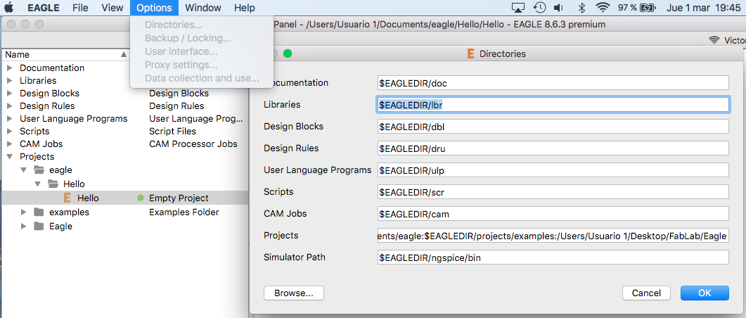
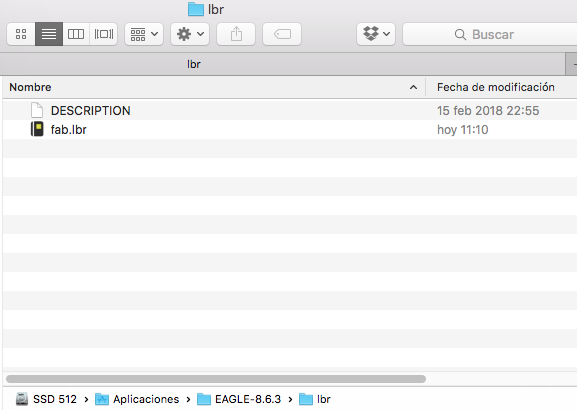
Installing the FabLab library: I went to the Resources repository and I downloaded the fab.lbr. I opened Eagle, I went to Options->Directories, in order to see where the libraries are stored; and then I went to that file and I pasted the fab.lbr there.
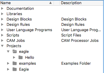
Eagle Menu:
- Documentation: manuals, tutorials...
- Libraries: where the libraries that come with the program and the ones you download are stored.
- Design blocks: create blocks of components that you are going to use frecuently.
- Design rules: you can establish the different parameters that your board will have like the distance between traces so the tool can cut them properly. The program comes with some os the ones that the enterprises have.
- Scripts: to automatize the tasks.
- CAM jobs: to convert to gerber, the format to be able to send the board to the companies. In my case I will use Fab Modules so I don't need this conversion.
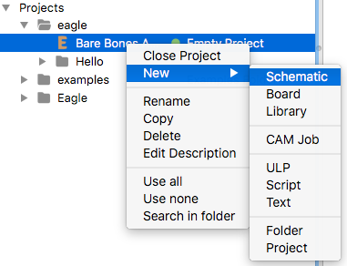
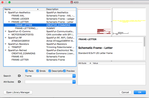
So, once I knew a bit what options the interface had I started to create a test project following the Sparkfun tutorial. I Right clicked on the Eagle file , where you can directly create a new Project or create a new file; in the new file Create new project -> Create an schematic: and save it.
It is important to choose what library you are going to use, as it is not needed to have all of them active. We can click on the right button in Managed Libraries and we turn on the fab.lbr library. And right click on Manage Library if we want to set it as Use none.
B. Creating the schematic:
Once you have opened the Schematic you can either click on the buttons on the left-side menu or you can just type the command that you are looking for and that tool will be activated. The main ones are:
- Add
 : the active libraries will appear in a new window. You search for the component you want to add, you click ok and you place it wherever you want in the schematic. If you are missing a component it can be because you forgot to click on
 usein a certain library that you needed. - Move and rotate

 : Once you have placed the components you move them in a logic way. All the ones that are related together.
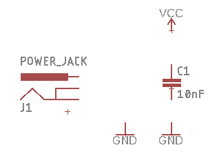
 - Net
 : Create the traces between the components. It is important to check that the unions have been done correctly. Important: don't mix up the
 LINE tool with the
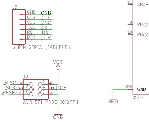
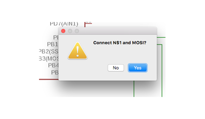
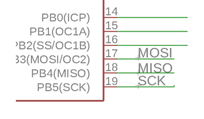
 NET one. To join components that are close to each other like in the first image, you just trace a net between them, but sometimes the components are far away from each other and to join them directly will mean to put a net across all the scheme. In this case, what we have to do is:
- Create a net from the pin that you want to connect to a point a bit ahead (like 14-19 in the 4th picture below).
- Use theName tool to change its name to what they need to be joined.
- You can put aLabel to be able to see it.
- And then you go to the components pat that will be join with that one, and you repeat the same process. When you add the name to the second one a screen will appear asking you if you want to connect it to the previous one (third image below). - Show: This tool can be used to check the connections you just did. In my case as I was joining different components in 'distance', by clicking to the GND of one of them, all the pats connected to ground will light up.
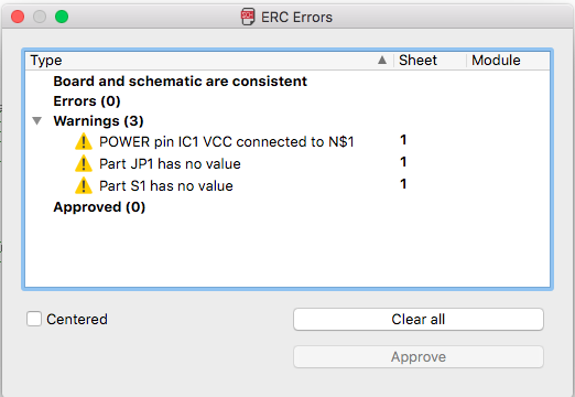
- ERC: it checks that all the connections are correct. When you click on it a new window will appear with all the errors and warnings that you have in the board. You correct them and then you can continue.
Useful tips that I learned and I will apply to the desing of my board:
- Place the crystal/resonator close to the microcontroller, in general, all the components that are related as closer as we can.
- One of the capacitors needs to be placed next to the microcontroller as it will be connected to the GND and the VCC to avoid noice.
- Avoid rectangular edges.
I have explained these previous steps with screenshots of the test board that I created following the tutorial.
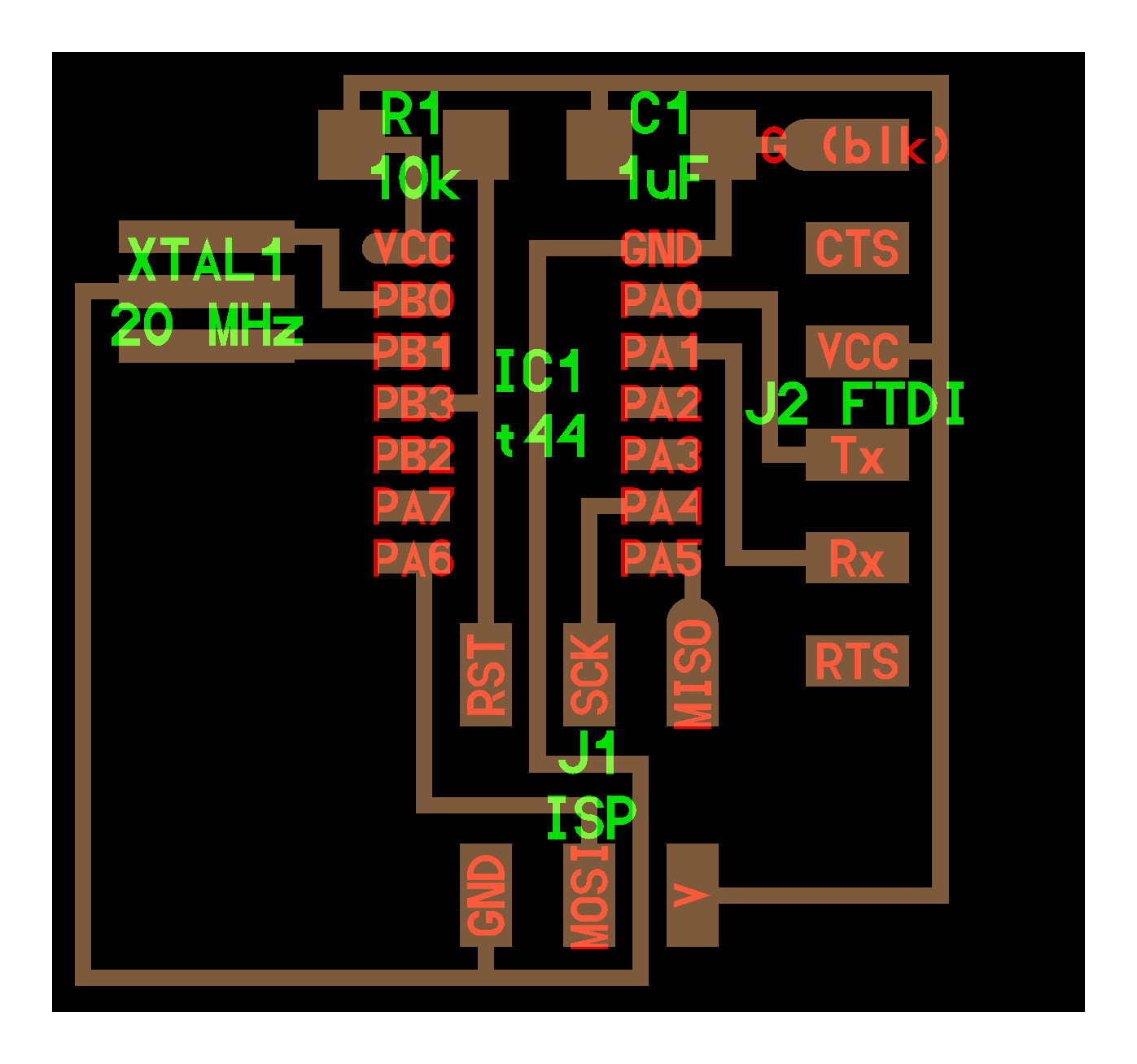
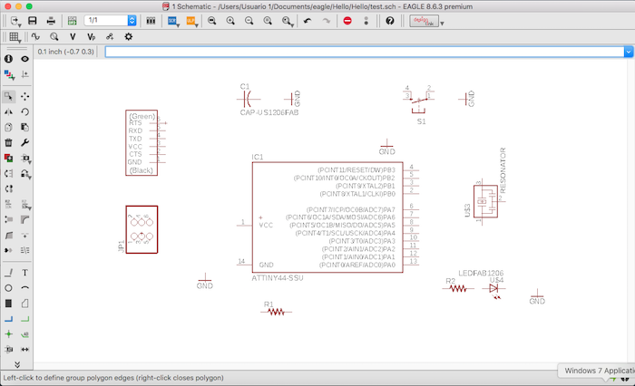
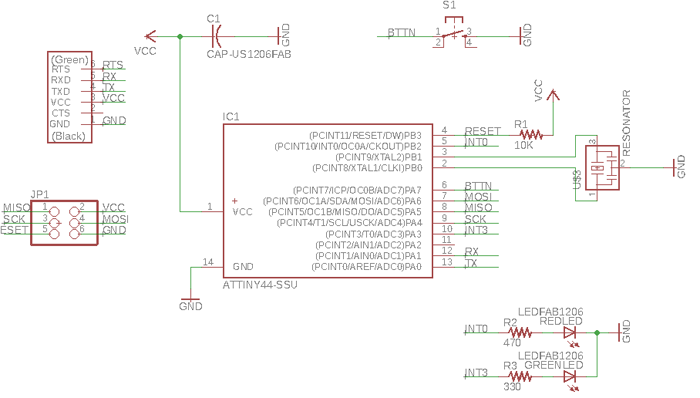
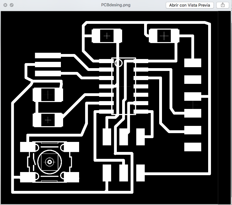
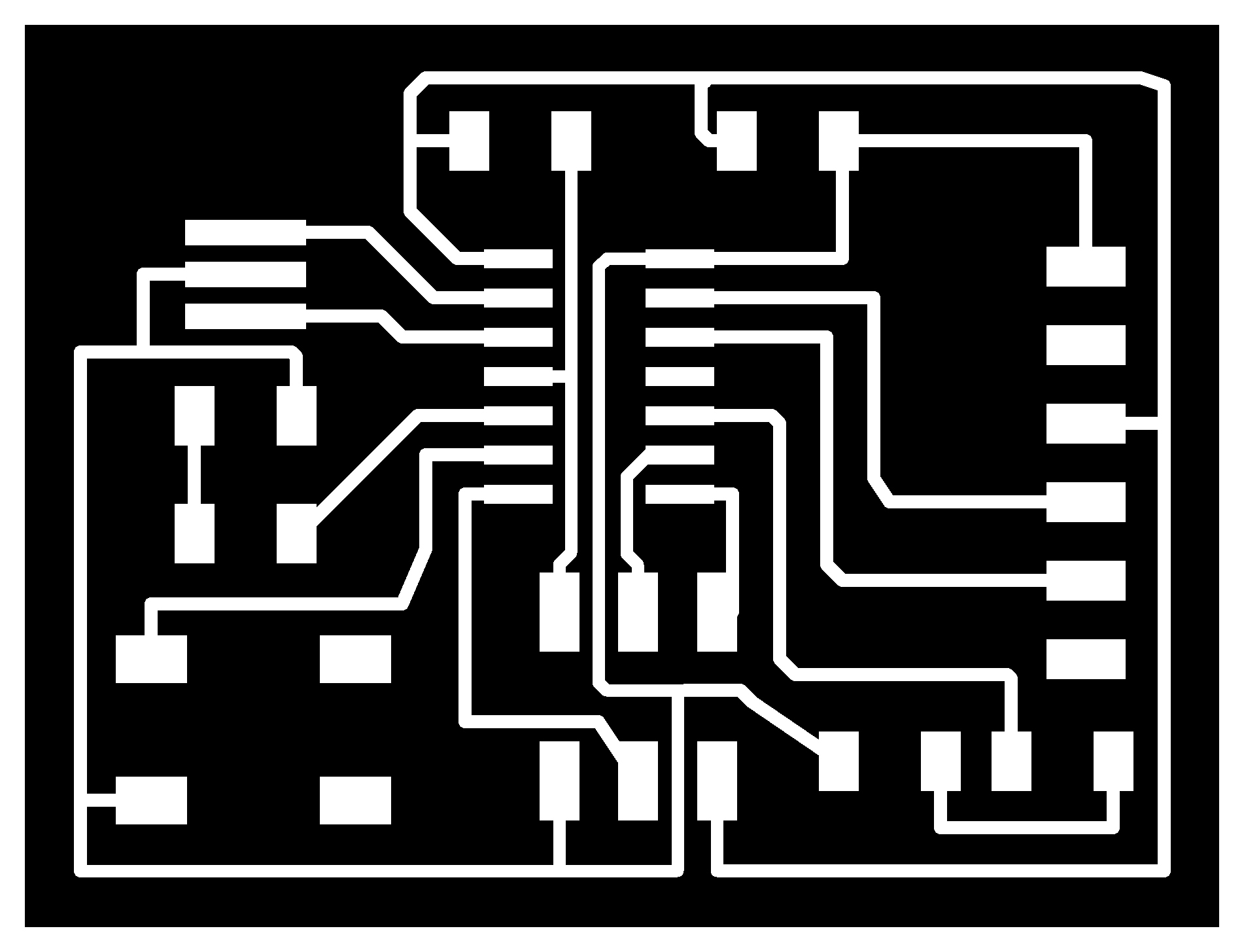
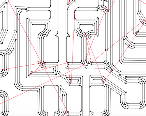
The resulting schematic of my Hello-world PC board is the following:
FIRST PROBLEM:
I did the next table because at the beginnign I was doubting about what components I had to include in my board and also what was their corresponding Digi-key link.
| # | Name | Desctiption | Link DIGI-KEY |
|---|---|---|---|
| 1 | Attiny44 -SSU | ATTINY44A-SSU-ND | Link |
| 2 | Head 3X2 pins(PINHD-2X3-SMD) | 609-5161-1-ND | Link |
| 3 | FTDI-SMD-HEADER 6pins | S1143E-36-ND | Link |
| 4 | Resonator 20 MHz | XC1109CT-ND | Link |
| 5 | Resistor 10Kohm (RES-US1206FAB) | 311-10.0KFRCT-ND | Link |
| 6 | Resistor 470 ohm (RES-US1206FAB) | ||
| 7 | Resistor 330 ohm (RES-US1206FAB) | ||
| 8 | GREEN LED of 1.8V (LEDFAB1206) | 160-1169-1-ND | Link |
| 9 | RED LED of 1.8V (LEDFAB1206) | 160-1167-1-ND | Link |
| 10 | Unpolarized capacitor of 1uF (CAP-US1206FAB (CAP-US)) | 445-1423-1-ND | Link |
| 11 | Button (6MM_SWITCH) | SW262CT-ND | Link |
The value that I choose for the resistance came form the calculations looking at their properties:
RED LED: 1.8V , 8mA
GREEN LED: 2.1V , 10mA
C. Creating the board:
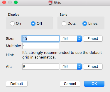
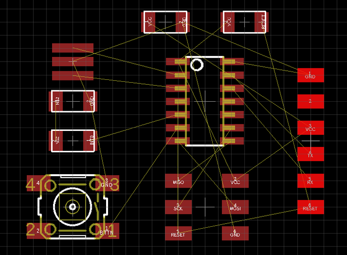
After checking that the schematic is correct you click on Generate/Switch to board. All the components will appear on one side of the board. As we did before it is good to show the Grid, as in this case it will be really useful by forcing the components and traces to match the grid that we have defined.
- Create a DRC:
Layers: you don't need to change anything as I will use only one.
Clearance: Change the default widths for the width of the tool, in my case 0.4mm.
Distance: I will leave it as it is.
Sizes:
- Minimum width: To be able to work with the modela we have to give a minimum width and spacing of 15.
- Minimum drill: 0.79.
Once you finish modifying these characteristics you - Move and rotate: as done before in the schematic, we need to place de different components on the board. In the Sparkfun tutorial that I followed they light up some basic rules to have in mind when arranging the components. These rules are:
A. Don’t overlap parts.
B. Minimize intersecting airwires: when you are moving the components you have to see how the wires are moving with them.
C. Part placement requirements: Some parts may require special consideration during placement.
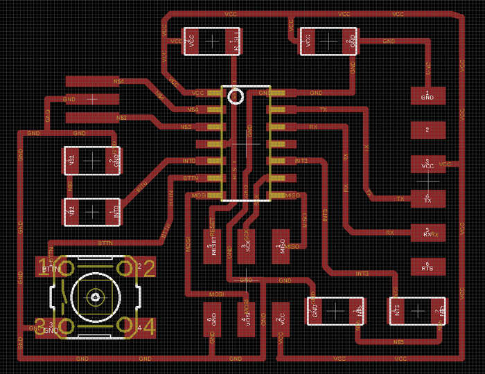
D. Tighter placement means a smaller and cheaper board, but it also makes routing harder. - Route: for drawing the traces between the components you select the part that you want to join and you go to the one you want to join. Change the width in the top menu to 16.
Activating the grid will make this easier. A correctsizeis 0.254mm / 10 mil andalt5 mil. - Adjust board size: Once the components are inside the board you move its the edges, so we dont waste board space.
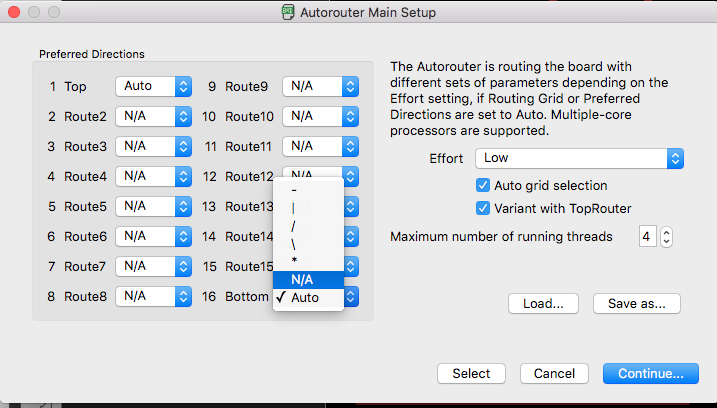
- Auto: Optimize the colocation of the components. If it gives you a percentage around 80%, it means that your board traces are correct, but a low percentage will mean that is not. In its window, change Bottom for N/A, as I only have one layer.
- Then you click DRC and check if the board fulfill the conditions that were establish at the beginning.
Save as....
Make sure you don't close one of the windows (schematic/board) because the program will give you errors.

PROBLEMS DOING THE BOARD:
I had some issues when drawing the traces because I started with the VCC and then I did the small traces between the microcontroller and the LEDS, HEADS..., leaving the GND the last one. When I went to connect the GNN to the components, I had a lot of conflicts and I had to erase some nets and re-do them. At first I was not aware that the traces could go trough the middel of the microprocessor!
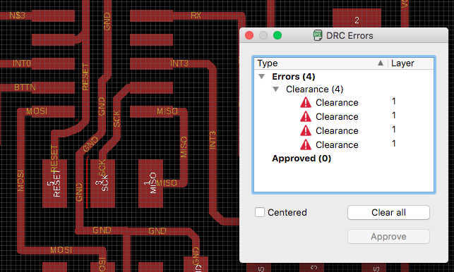
PROBLEMS WITH THE SEPARATION BETWEEN TRACES:
Once I had joined all the components I checked the DRC settings and I had to change some of the nets as they were very close to other components or other nets. You can see on the right side of the DRC window in the image that the GND net is very close to the VCC pad. I had some distance errors at this point but also when I went to mods, some of my traces were not going to be milled. (Picture in that section.)
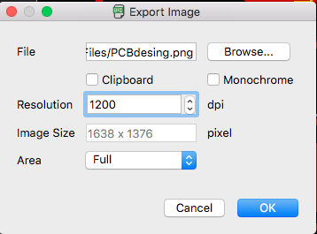
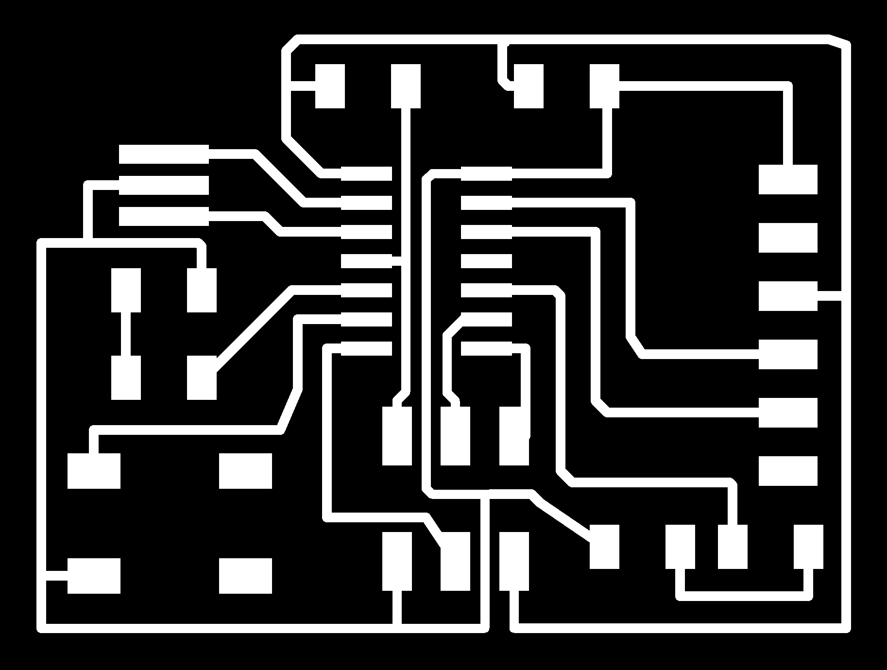
D. Exporting the .png file:
To export the file, you only need to select the traces and pats, in my case the Top layer, File->Export->Image: Check the Monochrome check box, give a 1200 resolution and then click OK.
PROBLEMS WHEN EXPORTING:
- When I exported the image, I first forgot to check the Monocrome box so the resulting image had the appearance of the one in the board interface.
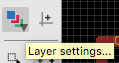
- Another mistake that I had was that when I exported it, the shape of the button and the microcontroller were appearing. The problem was that I used the command Layer by writing it and the resulting window was not the same as the one that you open when you click the Layer settings icon. So, when I was selecting the Top layer in the first way it was not working properly.
Once I had fixed all this mistakes I exported the final Image in the .png format.
E. Editing the .png in Photoshop:
Once you have exported the image from Eagle you open the image in an image editor, Photoshop in my case, in order to include a border for the Modela to cut the outside part.
- We make the canvas bigger, adding 1.6mm on each side, centered, and we leave the default background in white.
- You export this file as .psd just in case and as .png. = The resulting file is the traces one.
Then you do the outside file, you select the border and you fill it with black and you invert the selection to fill the inside with white.

3. Milling with the Modela:
Previous steps with the machine:
First thing I had to do was to press the ON button to turn on the machine. Once you have done that the machine will move to the right side and the board will come to the front. Then, in order to be able to change the location parameters in the computer we press the button VIEW.
- In my lab: Open two terminals (
ctr-alt-t), to start the server (cd mods -> http server -> sh start). - Go to the Mods website.
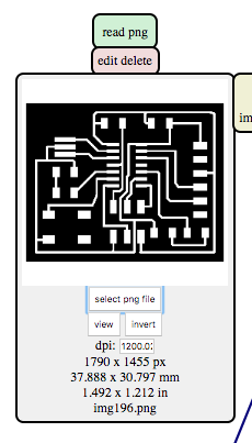
- Upload .png file and check that the dimensions are ok
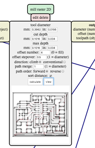
- Choose the tool you will use (1.64 or 1.32)
1- We choose the 1.64 to mill the traces.
2- Change to the 1.32 one in order to do the outside.
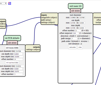
Parameters: dm, depth = we don't usually have to change them.
Offset = number of iterations that you will do engrave your shape: minimum 4 to have a proper separation between traces.
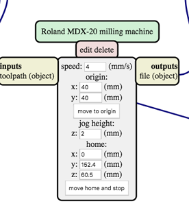
- Change the x and y position to the center of the board for calculating z0 position, I set them as (40,40). We leave the speed as the default.
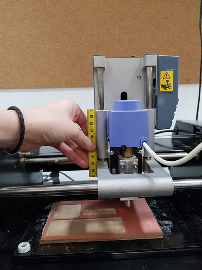
- You now press the
DOWNbutton in the machine until you have 0.5 cm distance in the head of the machine (see picture) - I released the screw, holding the tool, and I left it touching the board. Then I screw it again.
- As I was starting a new board I adjust the size to the bottom border, so the x-y position I wanted was (22,32).
- Then you click again the
move to origin. - And once I have the pointer in the desired x-y position you click again in
calculate, and you check that is going to mill properly the traces. When I was doing this step I realize that my traces were not going to be good. - SEND file.
PROBLEMS WITH THE TRACES:
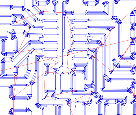
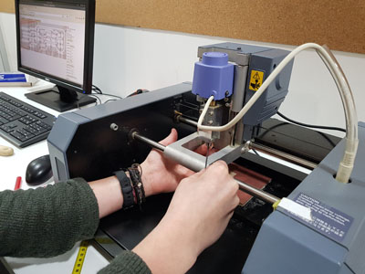
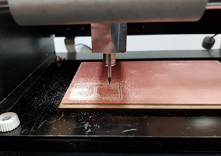
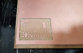
After checking all the traces and modifying the board in Eagle I send it to the printer and the boar was milled successfully. Here yo can see two pictures of the Modela.
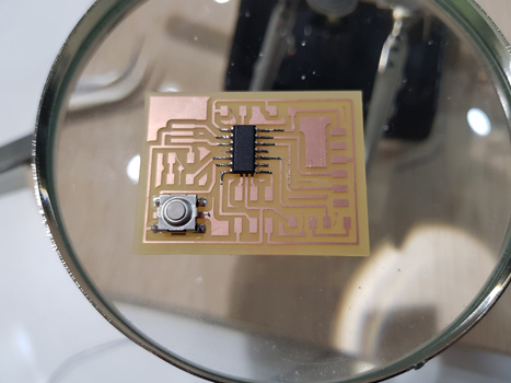
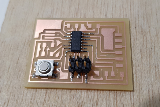
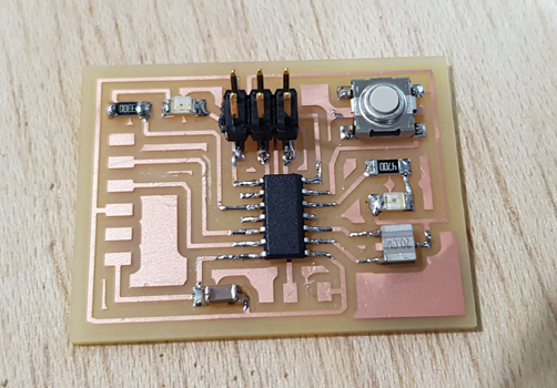
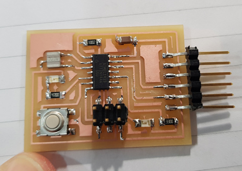
4. Soldering the components:
For soldering the components I had to look at the board design and decide in which order I will solder them and think about the positions of those components that are directional.
While I was soldering the components I checked the continuity of the components and everything seemed to be correct.
5. Programming the board:
I checked that the program was working in three different ways:
- Uploading the program to the board through the terminal.
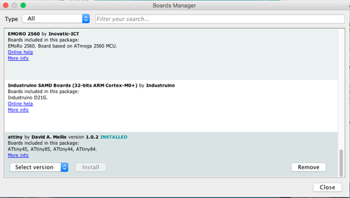
- With Arduino's interface. For working with arduino you first need to include the ATTiny in the board manager. For doing so you need to copy this link in
Aditional Board Manager URL, in Arduino's preferences. burning the Bootloader. Then, go toTools -> Board -> Board Managerand select the ATTiny thay will now appear thanks to the previous step.

Now the tools Menu should look like this. Change the board, processor, clock and programmer settings to have the ones you need.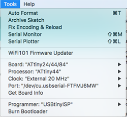
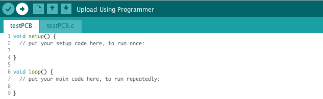
Then in order to be able to program the board in Arduino you need to Burn the bootloader the first time you are using it: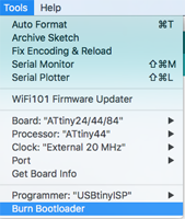 Then you write a code and you upload it to the board using the top left buttons of Arduino's IDLE.
 #include <SoftwareSerial.h> const int buttonPin = PA7; const int redLedPin = PA3; const int greenLedPin = PB2; int buttonState = 0; SoftwareSerial Serial(PA0, PA1); // RX, TX void setup() { Serial.begin(9600); // setting the LEDs to outputs and the button to output pinMode(redLedPin, OUTPUT); pinMode(greenLedPin, OUTPUT); pinMode(buttonPin, INPUT_PULLUP); } void loop() { buttonState = digitalRead(buttonPin); if (buttonState == LOW) { digitalWrite(redLedPin, HIGH); Serial.print("The red LED is on"); } else { // turn LED off: digitalWrite(redLedPin, LOW); } }
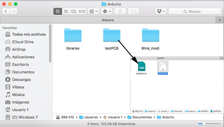
- Another wat of doing it is by adding the program written in .c in the file where I have a test program written in .ino so when I open this .ino program, both files will open and through the compilation of the .ino on the program is compiled.
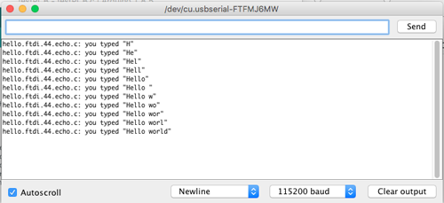
If you now open the Serial monitor of Arduino and you type some letters, you will have them printed.
I did the first steps that are required for programming the board on the 7th week, Electronics design, in the Programming the board section:
I downloaded the code files from the Academy:
- hello.ftdi.44.echo.c
- hello.ftdi.44.echo.c.make
- term.py
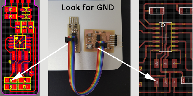
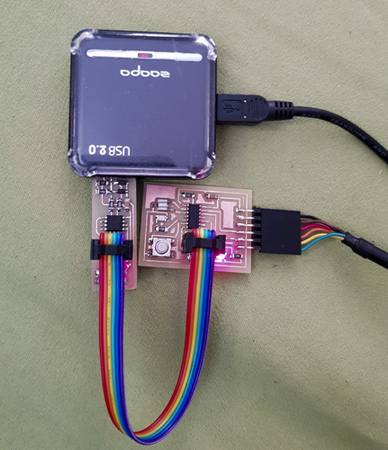
I connected both the programmer and my board to my computer and between them, using the FDI connections. When you connect the programmer and the board between them you have to make sure that the pins are ok connected. Check in the scheme where do they have the GND.
In the same way as I did when programming the programmer (Week 05), as the file make has the commands that I need to create the .hex file, I opened a new terminal, I went to the directory where I had saved the files and I wrote:
$ make -f hello.ftdi.44.echo.c.make
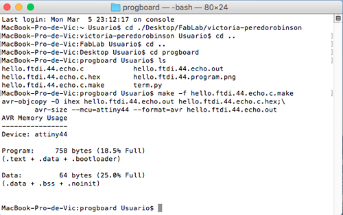
Then I executed the command that allows the creation of the fuses:
$sudo make -f hello.ftdi.44.echo.c.make program-usbtiny-fuses
Everything worked properly so I proceed to the next step:
$sudo make -f hello.ftdi.44.echo.c.make program-usbtiny
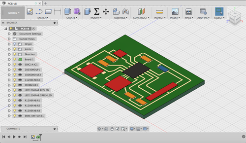
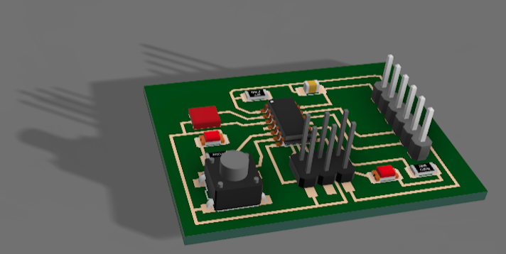
6. Extra credit: Rendering the board:
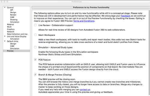
I created the rectangular base in Fusion giving it the size of the board. Usually you have to do it in the other way round but as I created first the board I will do it like this. I just created a rectangle of 40,26x30,8mm, and pull it a few mm up.
Then I went to Preferences -> Preview ->and check the PCB feature checkbox.
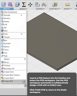
Then you go to the Create Menu->Create PCB. You choose the first option in the top menu PCB profile, selecting the sketch as the profile and the (0,0) as the origin. The board will change the colour to green.
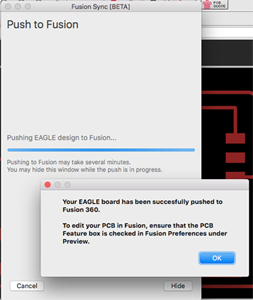
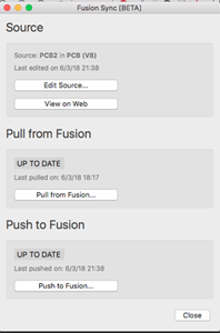
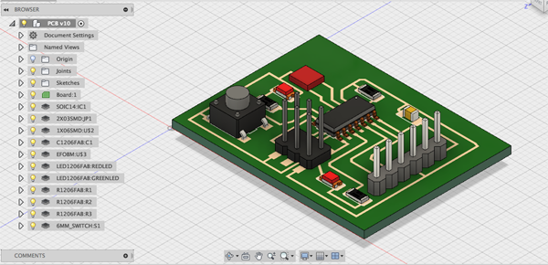
Now we move on to Eagle, you can find the steps in this Autodesk tutorial, and in the board interface you click on the Fusion SYNC, and check the Link to an existing Fusion design. There I pulled my design from Fusion and once it was done I clicked on push to Fusion. (Because before I put the shape of the board in Eagle, and then I 'send' the components to Fusion). As in my library the components don't have a 3D figure, for now in fusion you can only see the shape of them.
Now I will have to add the 3D figure of the components in the library and then push it again to Fusion for having the real rendering design. So, to do that, I created a new 3D library Right clicking on the desired library, Fab.lib in my case - > Create Managed Library. You wait until the library is created and then you right-click the new one in order to Open it.
Then, Edit 3D Package on Web, logging in with the Autodesk user.
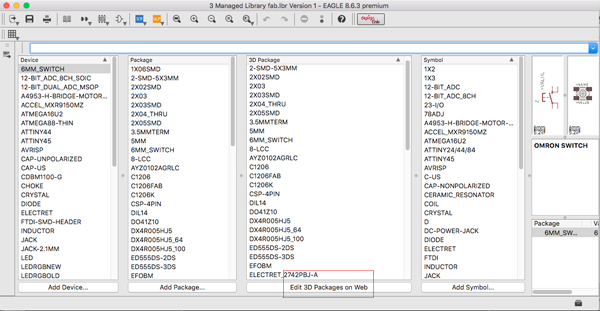
Go to package selecting the component you want to modify and then you click on Add model. When I opened this option I spend a lot of time searching for the components, and a realize that there is a window where it suggest you one shape and usually it was the one I was looking for. Once you have finished you have to refresh the library not only in the online version but also in the Eagle one.
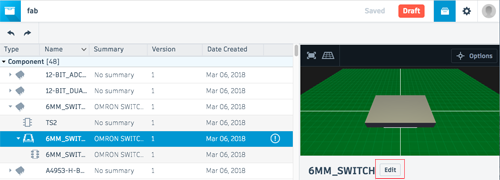
One you upload the component to the 3D model you have to Save it, Save a version of it, so when you go back to the online library it will appear in the top part Upload(#number of components you added).
Group assignment: Group assignment page
Measuring the board:
I used two devices to measure my board components. One was the Multimeter and other one was the Oscilloscope.
1. I first used the Kaise MY64 multimeter:
Measuring the resistance value: in order to check if they were working properly I used the 20K option to measure the 10k resistance and then the 2K to measure the led resistances of 470 and 330 ohms. You just need to move the wheel when the multimeter is switched off to the option you want and then place the plugs on both sides of the resistances.
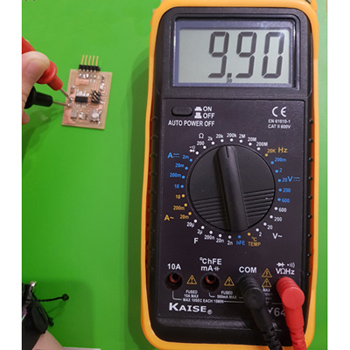
Measuring the voltage: I used the continuous current option to measure the voltage value between components. I measured from side to side of the LED using the 2V option.I also measured from side to side of the resistance observing, as is expected, a loss of voltage. I also checked that from the VCC to GND I had 5V.
Checking the continuity:
Is important to check the continuity of a circuit, not only to check that the components are really connected between them but also to check that we don't have a short-circuit. The way of doing this is by selecting the continuity symbol on the multimeter and placing the plugs over a trace or component connected to GND and other to VCC.

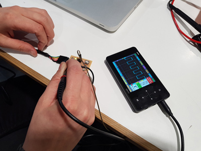
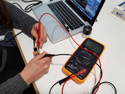
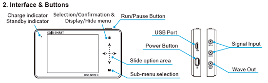
2. Then I used the Saint Smart Osilloscope DSO NoteII.
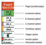
For using this oscilloscope we need to connect the probe to both ground and the part we aim to measure.
When I used the Oscilloscope I had compiled one of the example programs in arduino, the Blink one, to see how the signal in the oscillatory was changing. You can see in the square signal of the screen when the light was turning on and off.