 |
 |
 |
 |
Week5. Electronics Production
Assignments
group assignment:
characterize the specifications of your PCB production process
individual assignment:
make an in-circuit programmer by milling the PCB,
then optionally trying other processes
1. specifications of PCB production
| General Uses | Equipments and Tools |
|---|---|
|
 |
|
 |
Consideration for PCB layout. |
 |
2. An in-circuit programmer PCB hardware making
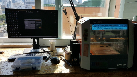
Step1. PCB milling
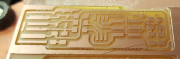
I did follow Brian's ATtiny45.
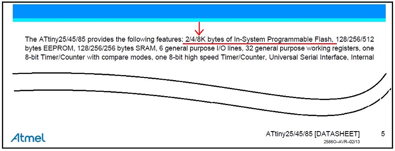
But I change mcu to ATtiny 85 device. I just want to expand buffer size to make speed up while downloading
from computer to target mcu board. Follow the datasheet, I found that Attiny85 has double size of flash memory compare than
Attiny45 device that is the reason why I change the mcu.
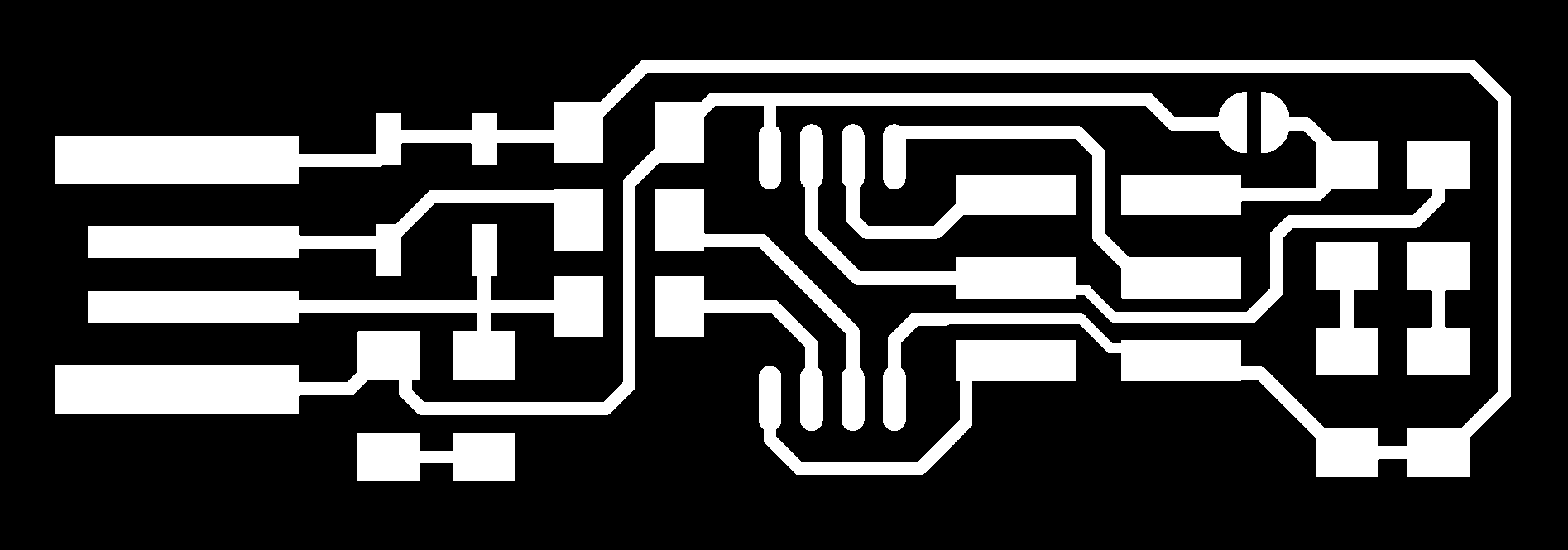
File download
Fabisp Traces(1000 dpi->*1)Fabisp Outline Outcut(1000 dpi ->*1)
*1. The resolution depends on how many pixes were designed for layout imge file.
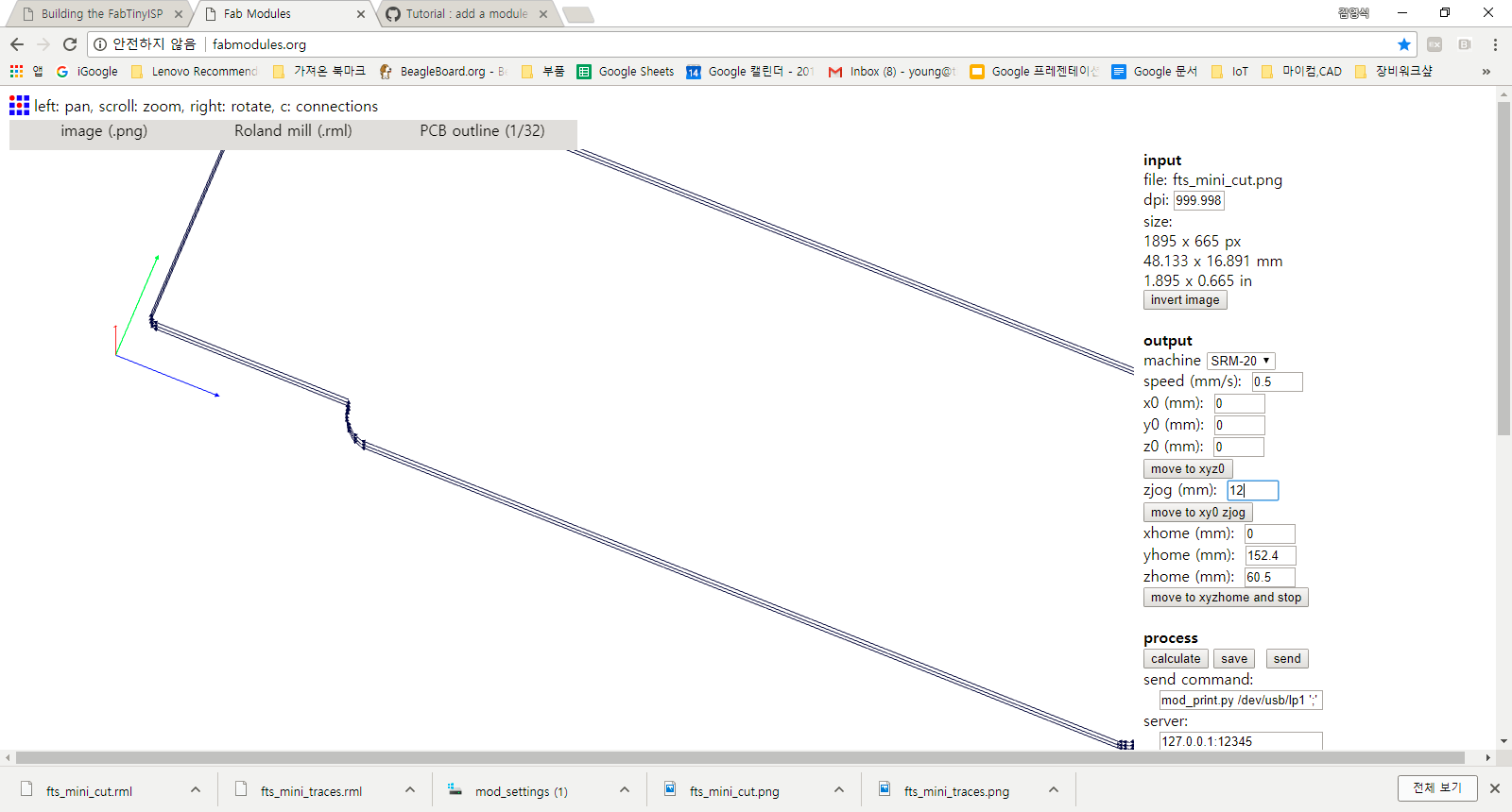
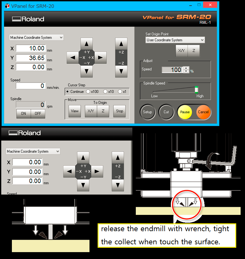
Before the milling the PCB, we needs the gcode files as .rml format for SRM20.
I did these works in fabmodules as shown below, I wrote about detailed parameters below the images
make data files in fabmodules
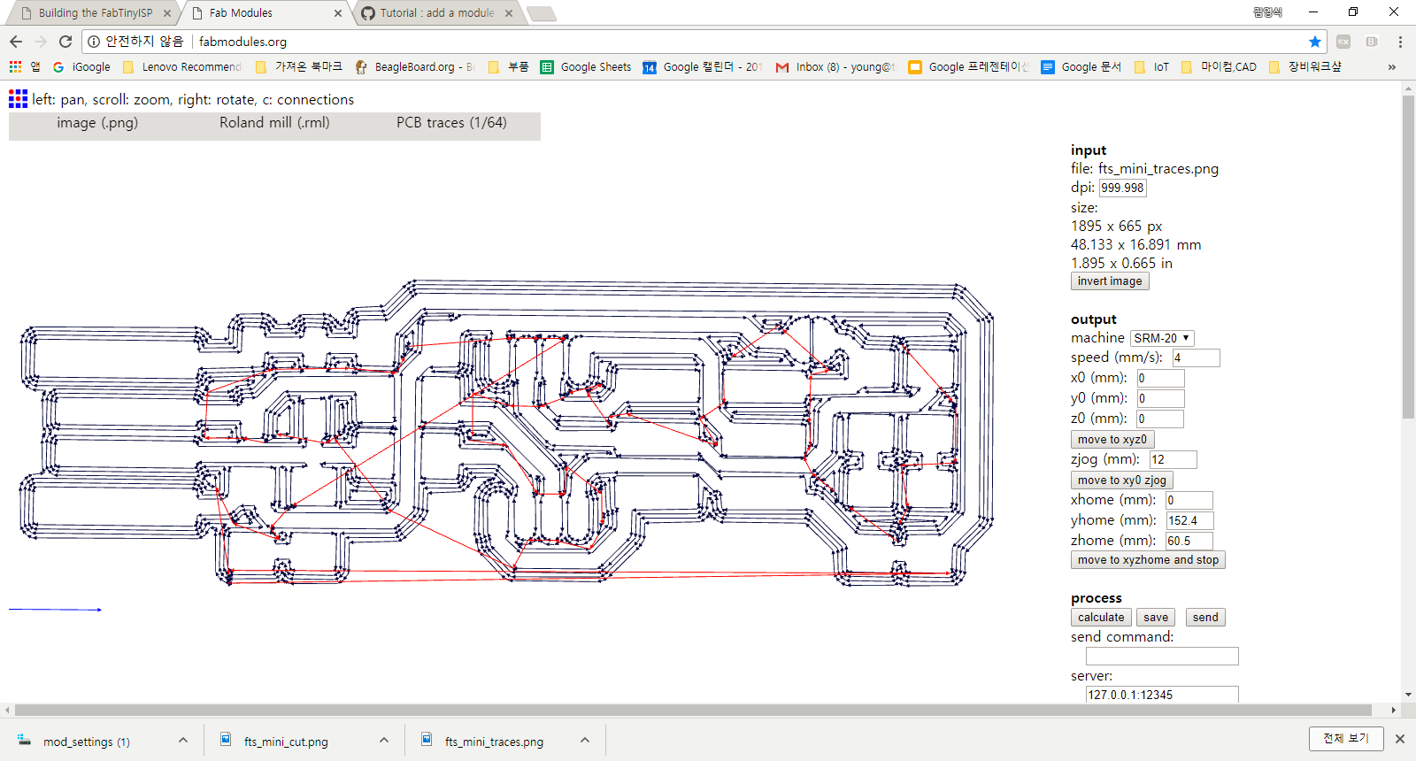
- trace cut work : Speed 4, X0=0, Y0=0, Z0=0, zjog=12, number of offset=4
- outline cutout work : Speed 0.5, X0=0, Y0=0, Z0=0, zjog=12, number of offset=1
Here I explain about PCB milling process as 4-parts.
board cutting process
| Procedure | Check | Caution |
|---|---|---|
1. PCB Setting |
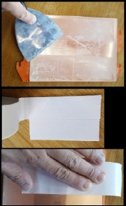 |
Carefully handle the PCB. Do not make a fingerprint on the copper surface |
|
2. Trace Cut(
for : cut the electronic circuit patterns
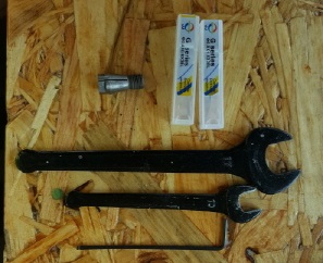
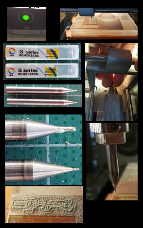
on copper layer) a. Check about machine. - Press the power switch(check about lamp). - Check about substrate assembling state. b. Endmill preset. - Screw the 1/64" endmill to correct collector. - Adjust endmill length of z-axis for preset. (In doing origination, can do make correct position.) c. Find and set the x-y origin point to air-cut. -In Vpanel software, slitely lift-up the endmill position (z-direction) , going to x-y origin point where to make board area and set the 'X/Y'button on top right side of software screen use with the x-y direction button. (refer to *Pic-1) d. Air-Cut - First load to work file on Vpanel. - Run a air-cut to check about following state via tool path. e. Set to Z-origin -Finally, goes down endmill in z-direction near about surface (never touch that doing control button press. wait before about 5mm distance - refer to *Pic-1) - Release the endmill to touch the surface naturally then tight to collect with 2 mm L-type wrench. In this position press the 'Z' button to set the z origin. And finally make that 3 dimentional origin point. e.Run Tracecut Just a lift up about 10mm, run the tracecut. And vacuum the milled surface with vacuum clearner. |
 |
If some errors were there in air-cut, check about the trace file. If something wrong in trace mill, stop the mill and check about origination. |
|
3. Outline Cut what for : cut the outside of board on CCL - Change the endmill to 1/32", load outcut file and set to z-origin. - lift-up the z-position of endmill then run the cut. |
|
Pic-1
Step2. Electronics Assembly
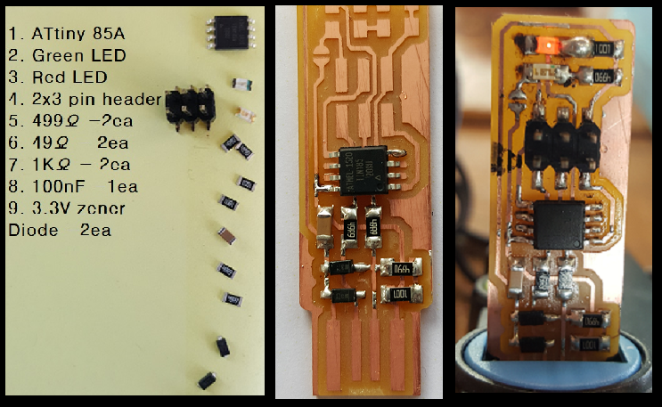
1. Prepare electronics parts.
2. Place the parts and solder all electrodes.
3. Inspection all parts put on the PCB, then simply connect to USB power to light on.
The reson of mill board instead of etching board.
- When we needs a proto-type PCB and a small amount of quantity then the mill process,
it gives more efficiences than commercial chemical production.
-Also, compare to etching methods for manually, it has extra some environmental pollution
even though exist that problem in materials manufacturing.
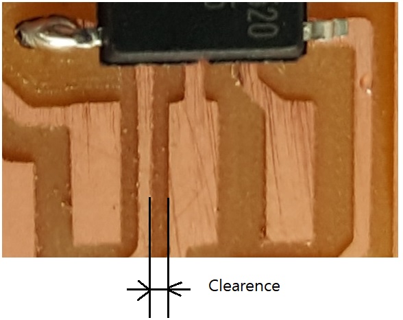
- First of all, its a solution about proto-typing for small size of integration of circuits,
except the clearence limitation.
3. fabISP firmware writing
Step 1. Construction of Software Tools Environments
We use ATtiny devices(from now microchip known as Atmel before).
I needs tool chain for Windows 10 OS, so I would prefer to follow install guide.
The tools are:
-1. AVR 8-bit GNU Toolchain3.5.4 : gcc compiler for Microchip(AVR family) microcontroller(i.e. mcu).
-2. GNU make-3.8.1 : Utility program for writing on mcu.
-3. avrdude : Making programmer for integrating of work files.
-4. Zadig 2.3 : USB driver installer.
Check about tools state after install.
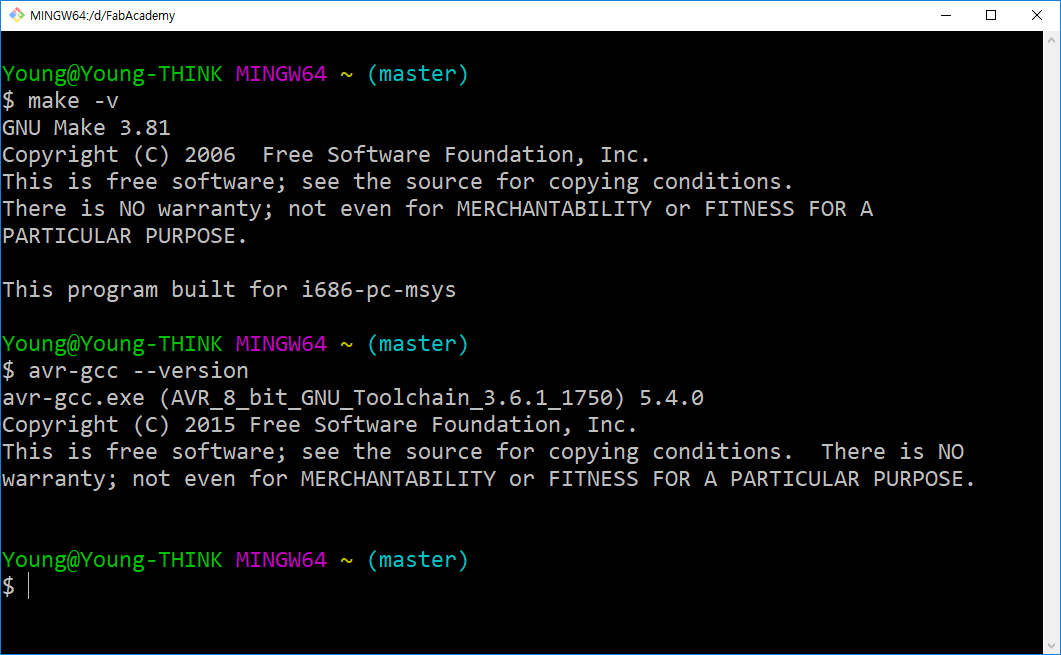
GNU ToolChain updated.
Step 2. Fabisp usb driver install.
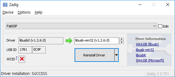
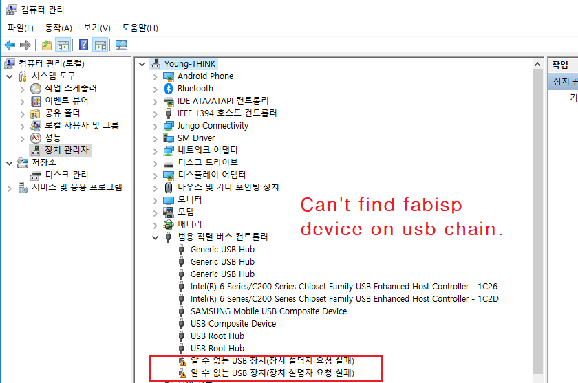
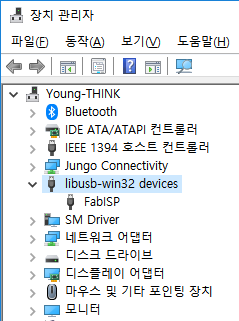
To make fabisp programming, It need connect to master fabisp device. then use Zadig utility.
Find FabISP device,and driver change to libusb-win32(v 1.2.6.0). But it didn't mapping correctly
in USB list on check System Device Manager.
Step 3. Sanity check
I several try above process, there are no evidence correctly configure.
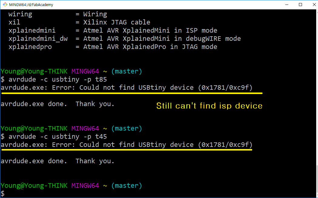
isp identification process
-usb port-avrdude check methods
Here after parts complished on week7.
Step4. recognize the fabISP on my Computer.
I did several times do the same procedure that makes to download 'libusb-win32(v1.2.6.0)' driver
on my computer(it is a USB driver, not COM-port serial driver).
And, just make sure MCU designator to 'attiny85' in Makefile.
Next I did initialization on command screen and check on Windows Device Manager what sign came on.
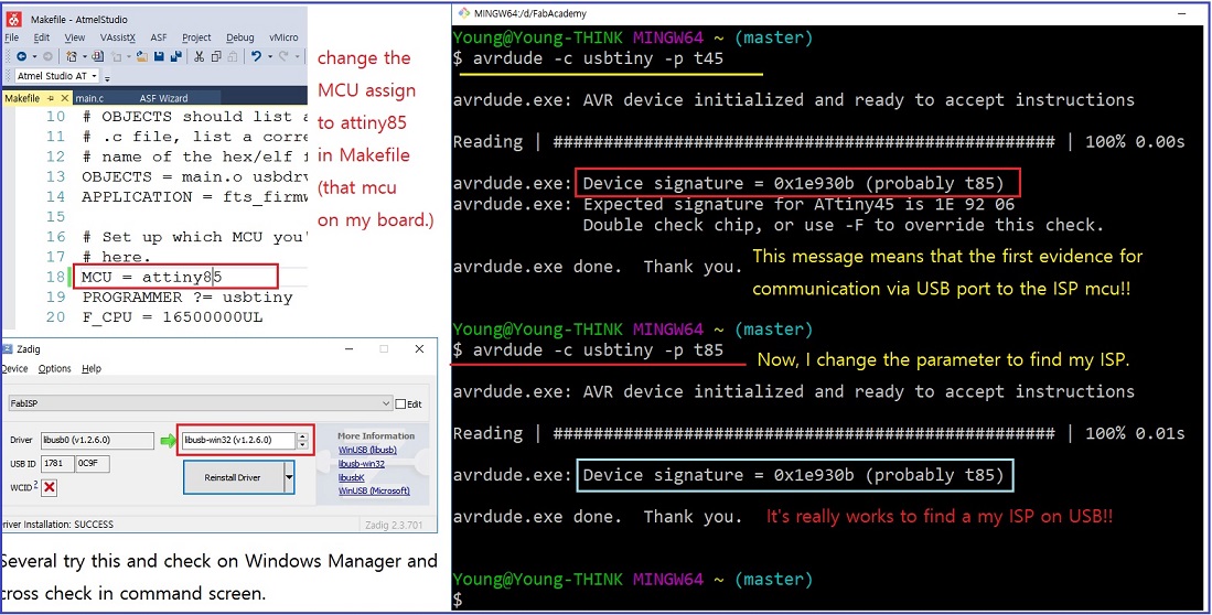
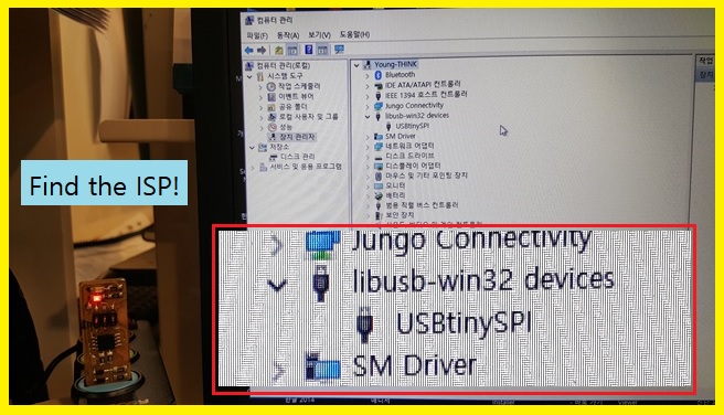
Finally to find on that device sign on my computer. here is the capture screen that link to my ISP.
After do this, I did upgrade from 'FabISP' to 'USBtinySPI' shown as below right.