 |
 |
 |
 |
Week7. Electronics Design
assignment
group assignment:
use the test equipment in your lab to observe the operation
of a microcontroller circuit board
individual assignment:
redraw the echo hello-world board,
add (at least) a button and LED (with current-limiting resistor)
check the design rules, make it, and test it
extra credit: simulate its operation
extra credit: render it
1. ReDesign Hello-world board
Software : KiCad
* note : Stable version is recommanded, but, I'm using nightly development builds version.
Reference design
Download materials
- Hello-world board schematic
- KiCad Library(scroll down to circuits section)
Schematic design
At first library files store to project folders, then register to software modules(Schematic Layout editor/PCB layout editor).
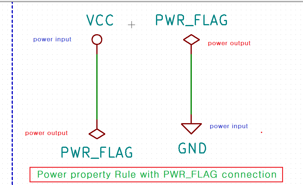
In KiCad schematic editing, need to be connect Power symbol to PWR_FLAG.
That module check about this for ERC run.
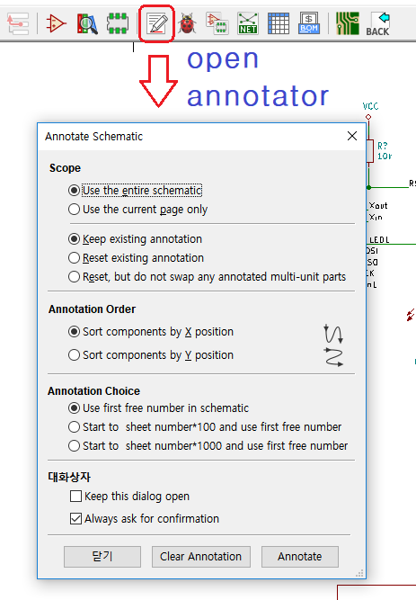
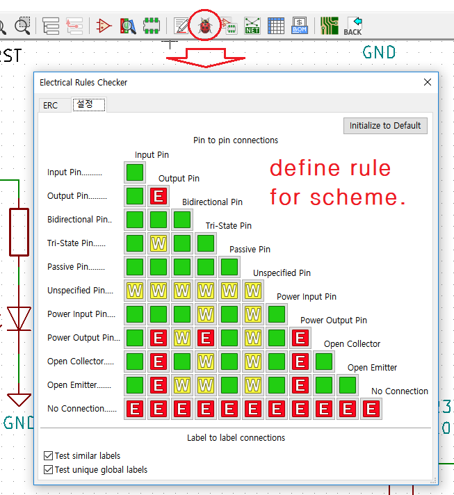
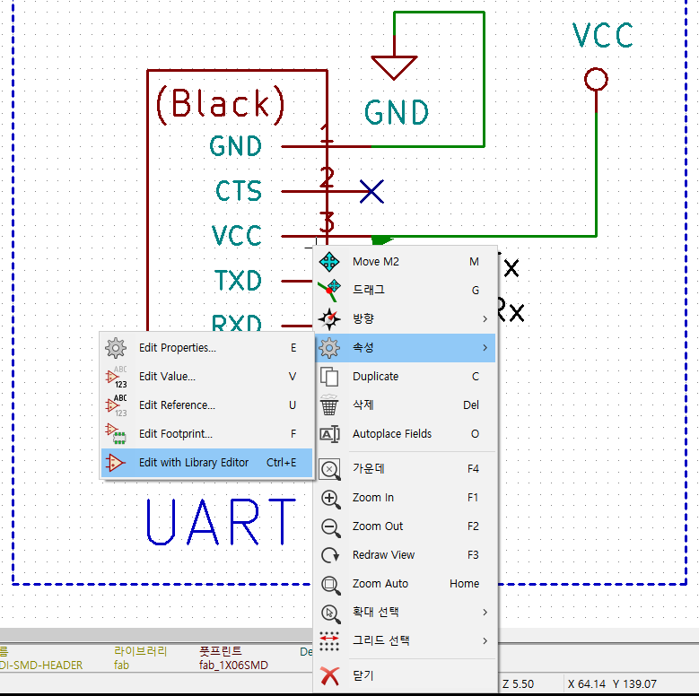
annotate each symbols to get id numbering, before netlist generation, check for electrical Rule check.
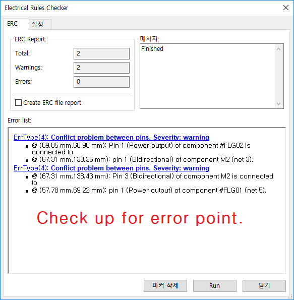
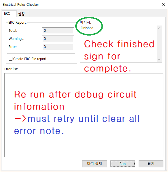
here are some errors, Follow to indication, find error dagger, that means mismatching electrical type.
i.e. Power Symbol must have Power input property and PWR_FLAG need to have Power output property.
in my drawing, PWR_FLAGs property was Bidirectional type set, so edit symbol property correctly.
here is my complete drawing.
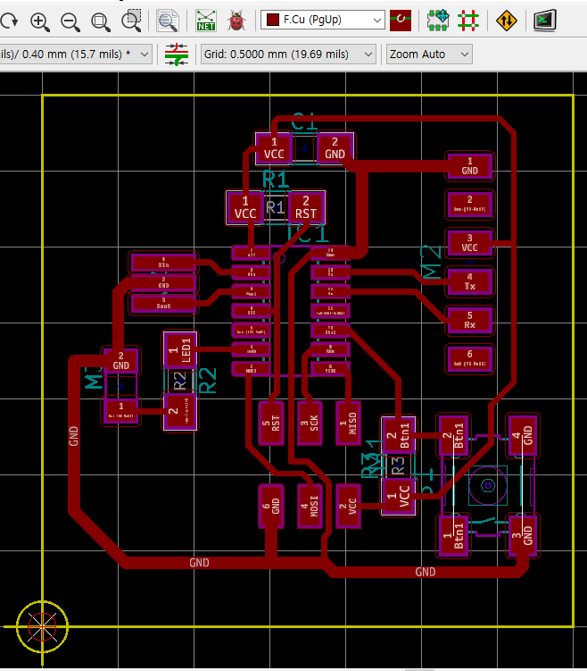
PCB artwork design
In Footprint editor, add 'fab.mod' file to use current work process.
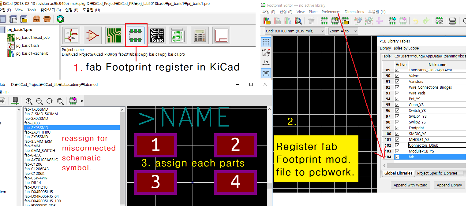
Load netlist file from schematic to place with linked footprints of previous added.
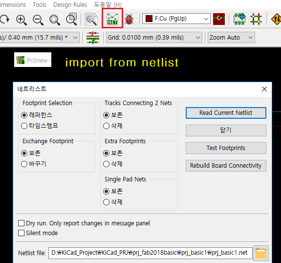
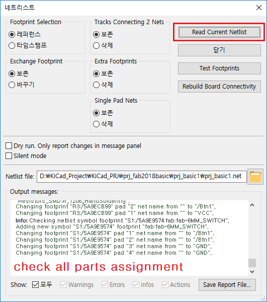
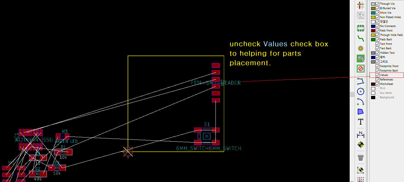
Check about all parts placed correctly, then draw a simple out-line for PCB outcut mill.
Artwork and make .png file to use in fabmodules.
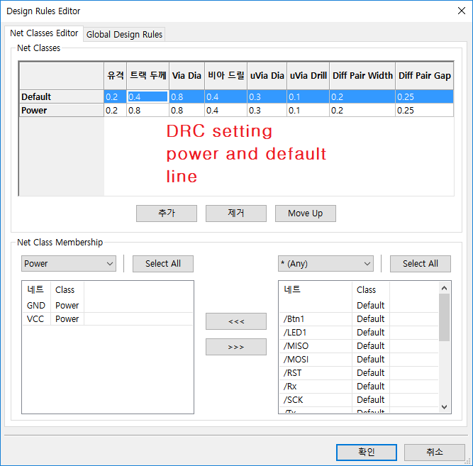
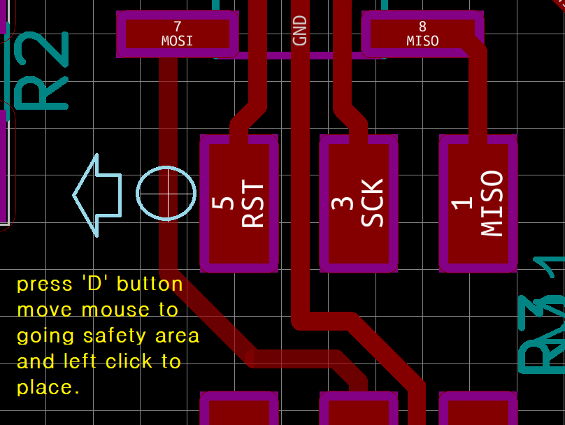
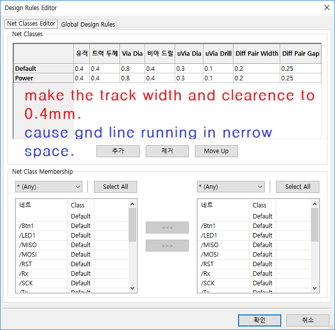
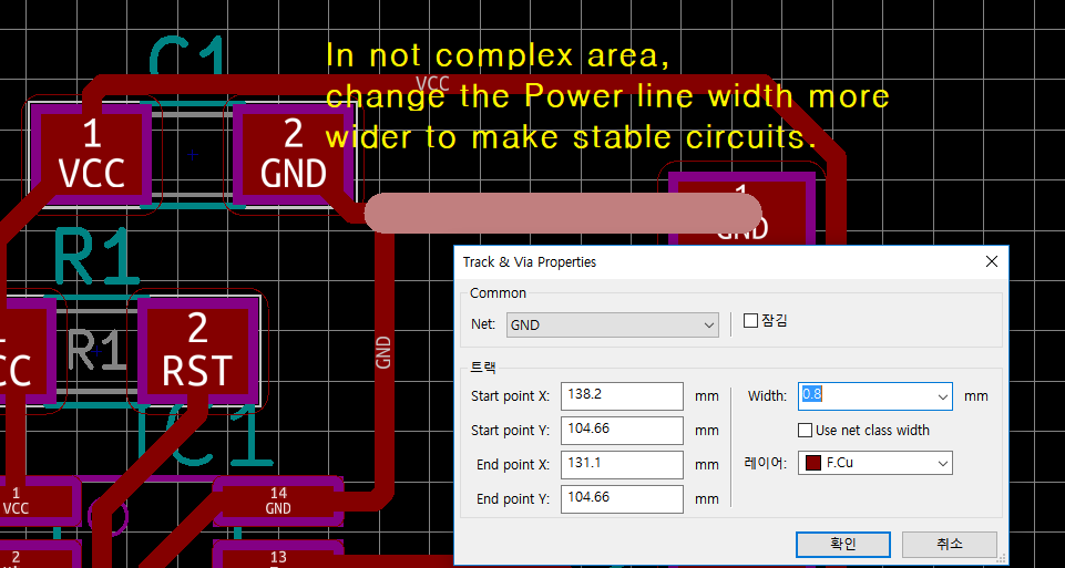
given DRC clearance default set is 0.2mm, it makes some lines conflict near pads.
I made a rule clearence to be 0.8mm but, in this design need to more narrow way to join,
I will try change to 0.4mm and fine control line spacing.
Here I choose .png file to make mill data. First export .svg file can be read in Adobe illustrator.
It is appear line thickness too big. Reduce weight so clear find circuit. But, all thickness has the same thickness.
So, make png format output and remapping width in windows paint program.
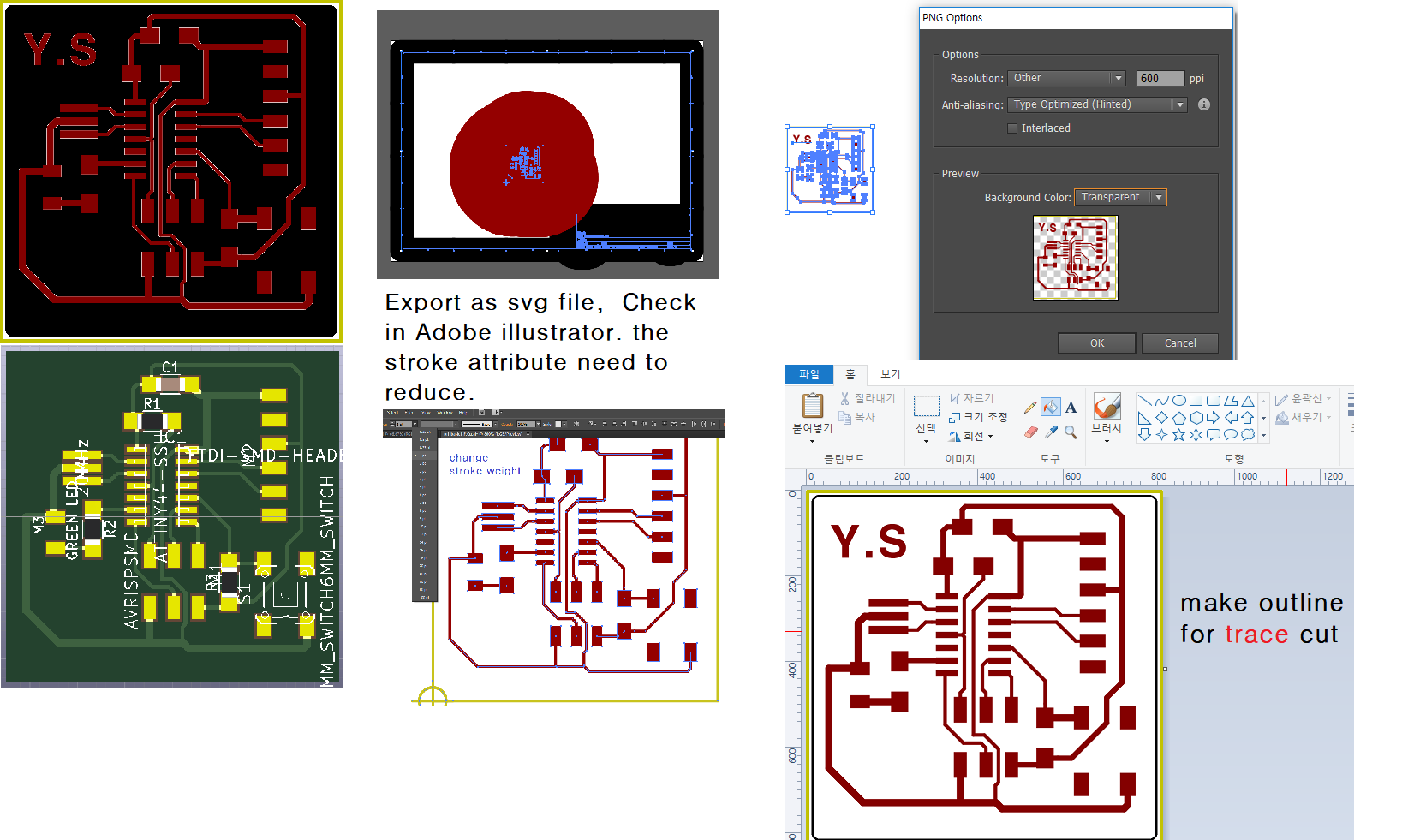
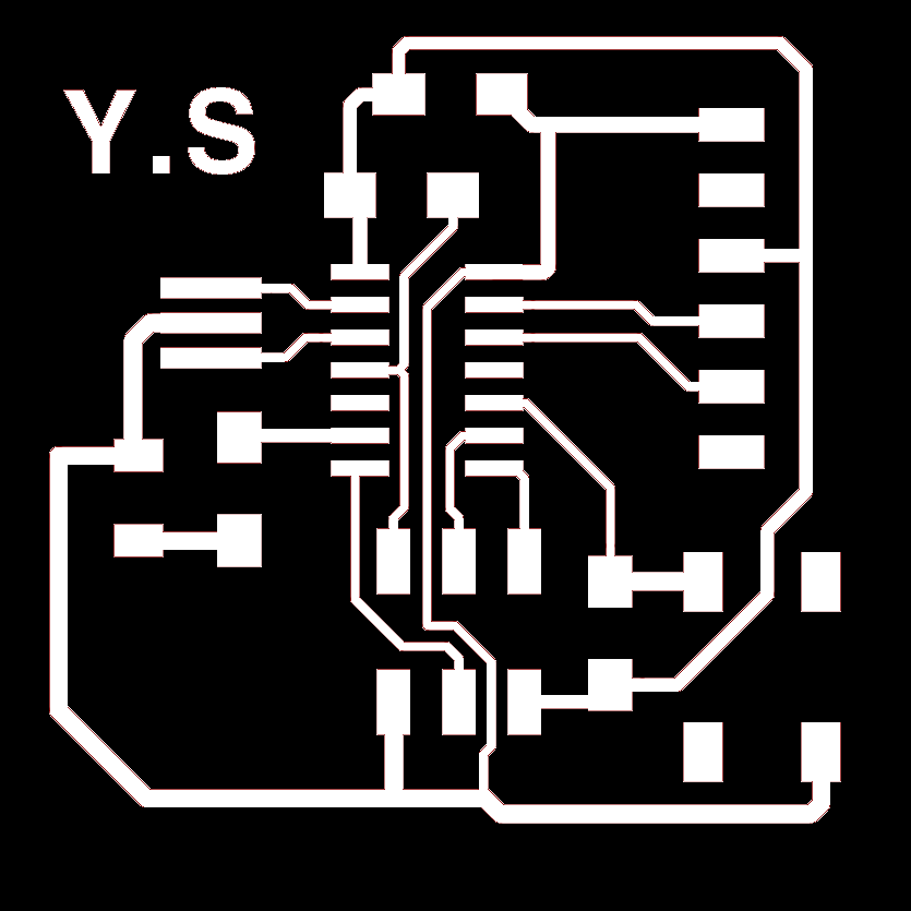
Now, divide trace pattern and outline pattern.

download files:
- trace image file:prj_basic1-F.CuToptracereverseR.png
- outline image file:basic1_outline.png
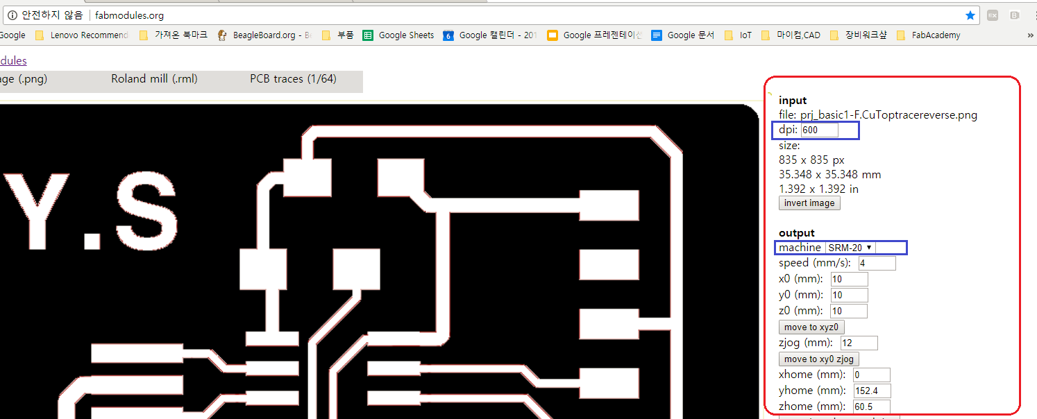
2. Making Board
Making milling work file
Before setting up parameters, check about dpi(dots per inch) relation. Wrong dpi value makes different board size.
Then machine status check before mill.
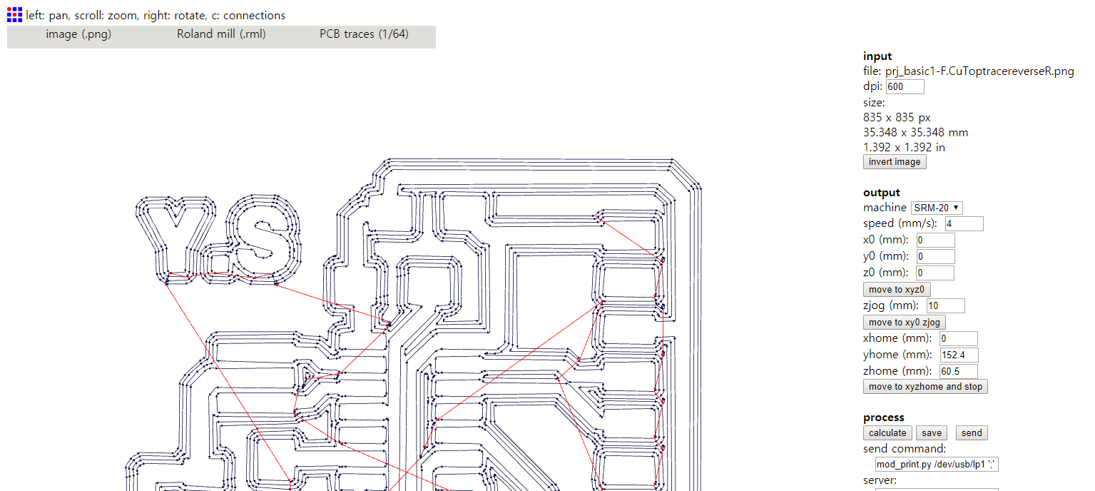
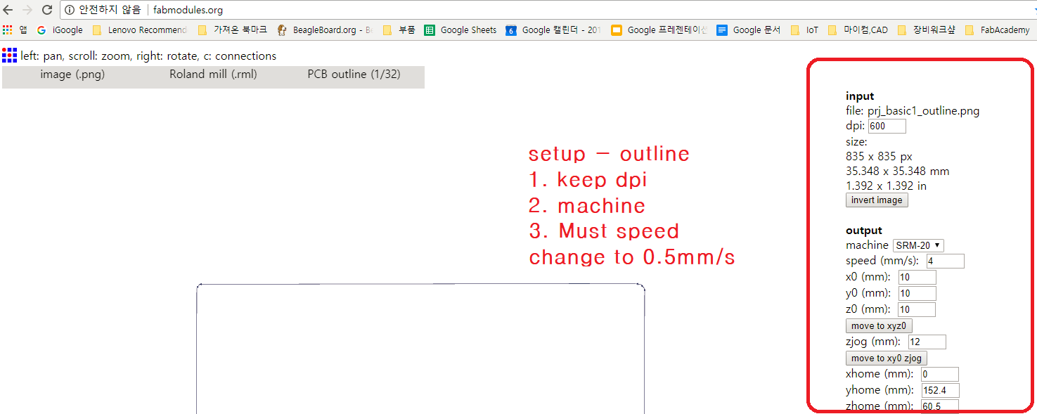
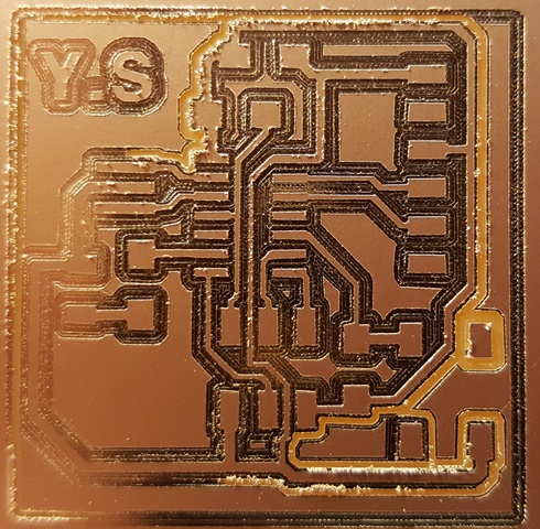
1st Milling
Error check and fix
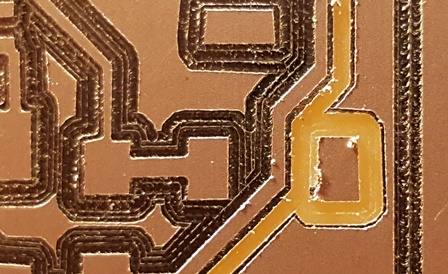
I found some errors on depth cut(Z axis), first for trace cut, most area didn't cutting
also outline cut seems to be left up.(compare to 2nd cut on the right.)
2nd Run
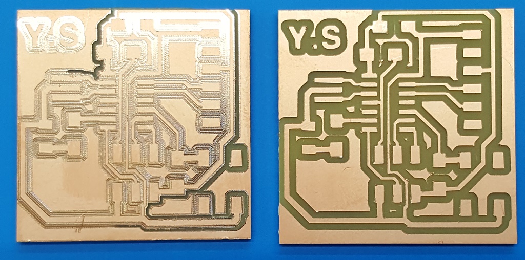
For the 2nd cut, I check several times on fabmodules and make sure z-origin point on SRM-20.
Other error fix
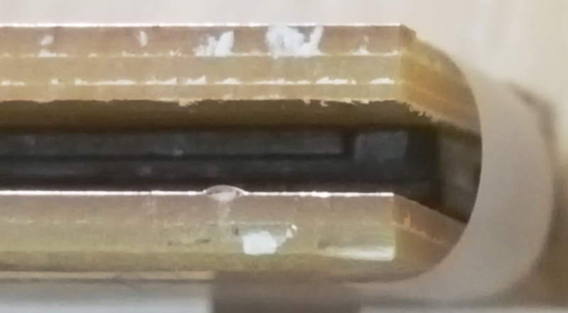
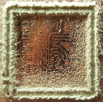
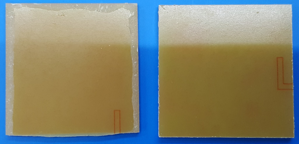
I realize 3 times cut to mill through depth, for under cutted 1st pcb still hold near plate,
so it's hardly to get off cutting pcb. Also I found broken parts remain near plate.
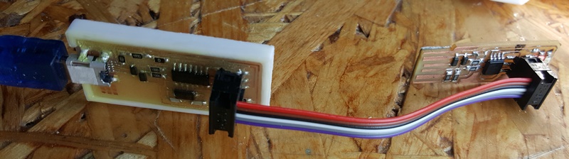
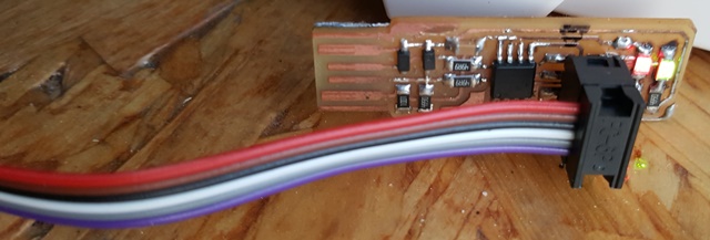
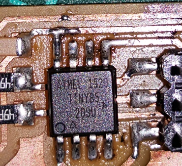
Soldering
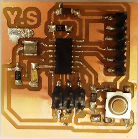
3. Programming and find a result
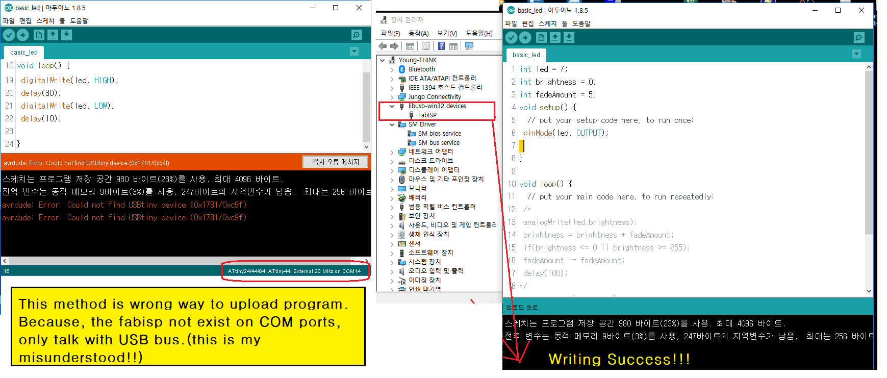
Prepare fabisp module
Detail process on computer, I'll descrive go back to week5 assignment section.
Fabisp plug-in to Arduino IDE 1.8.5
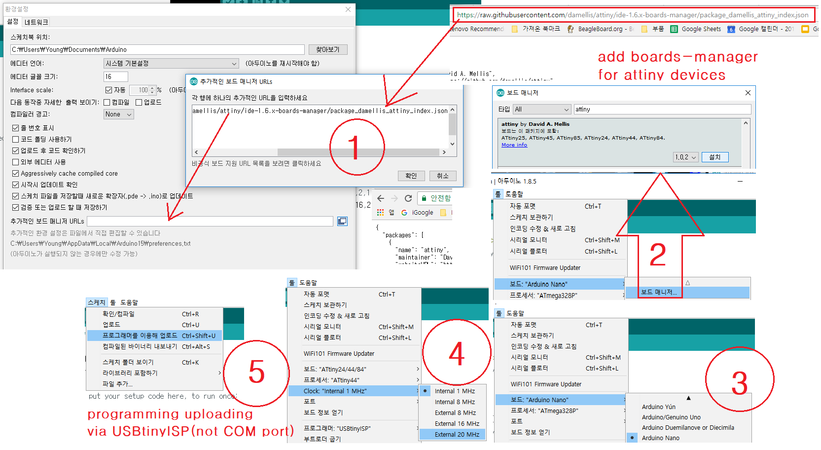
Programming, download and result.