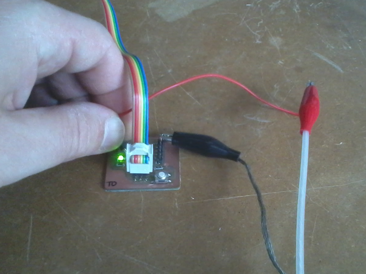
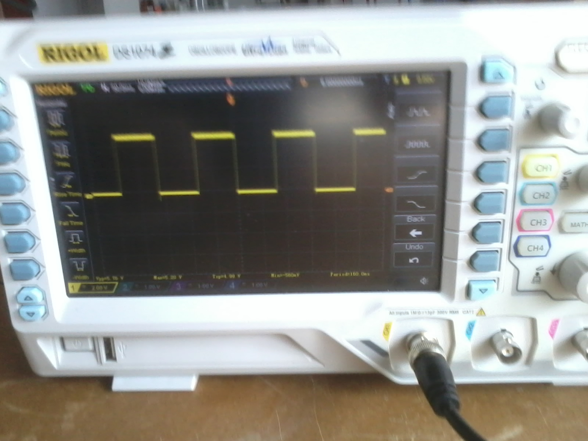
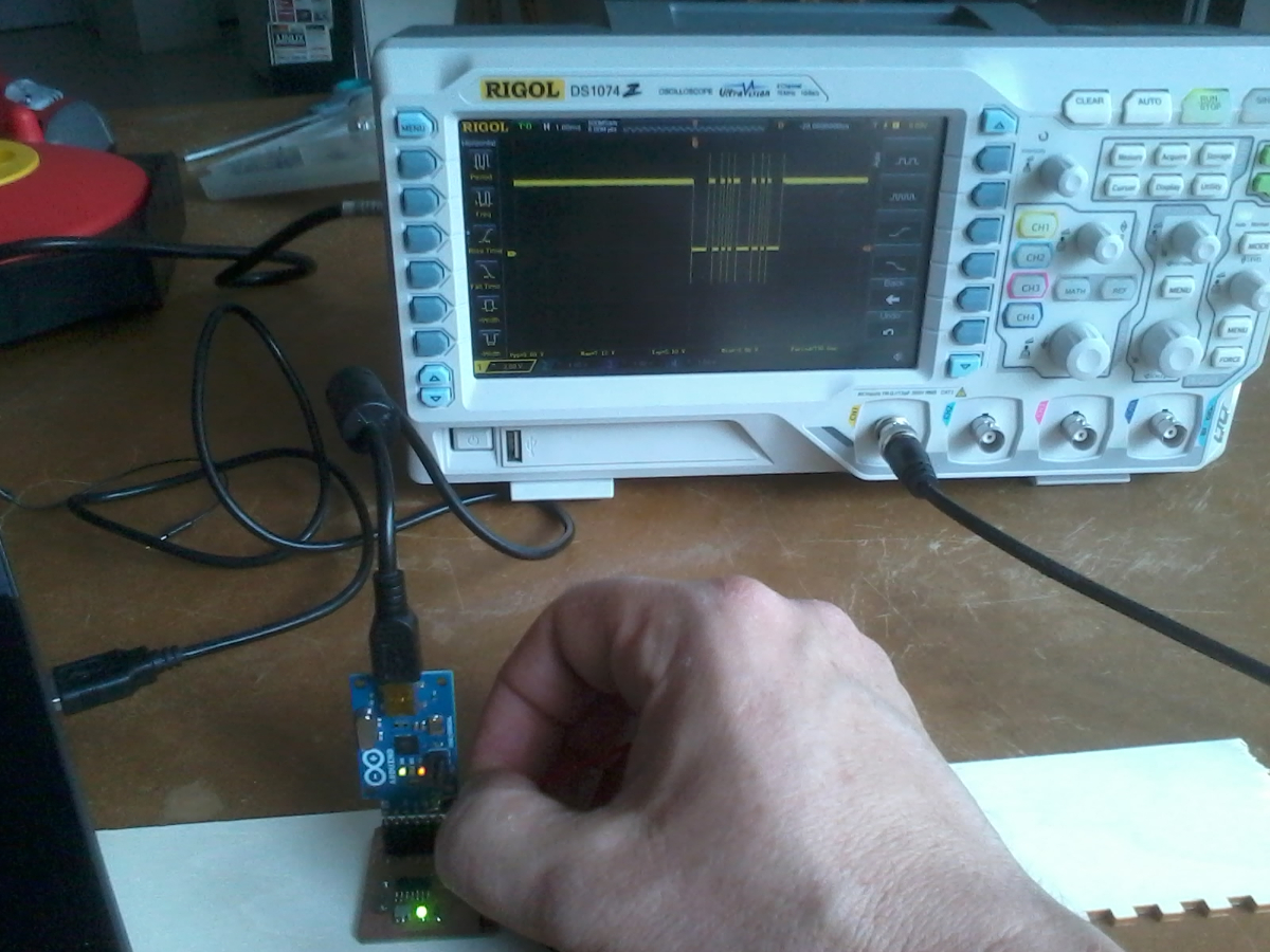
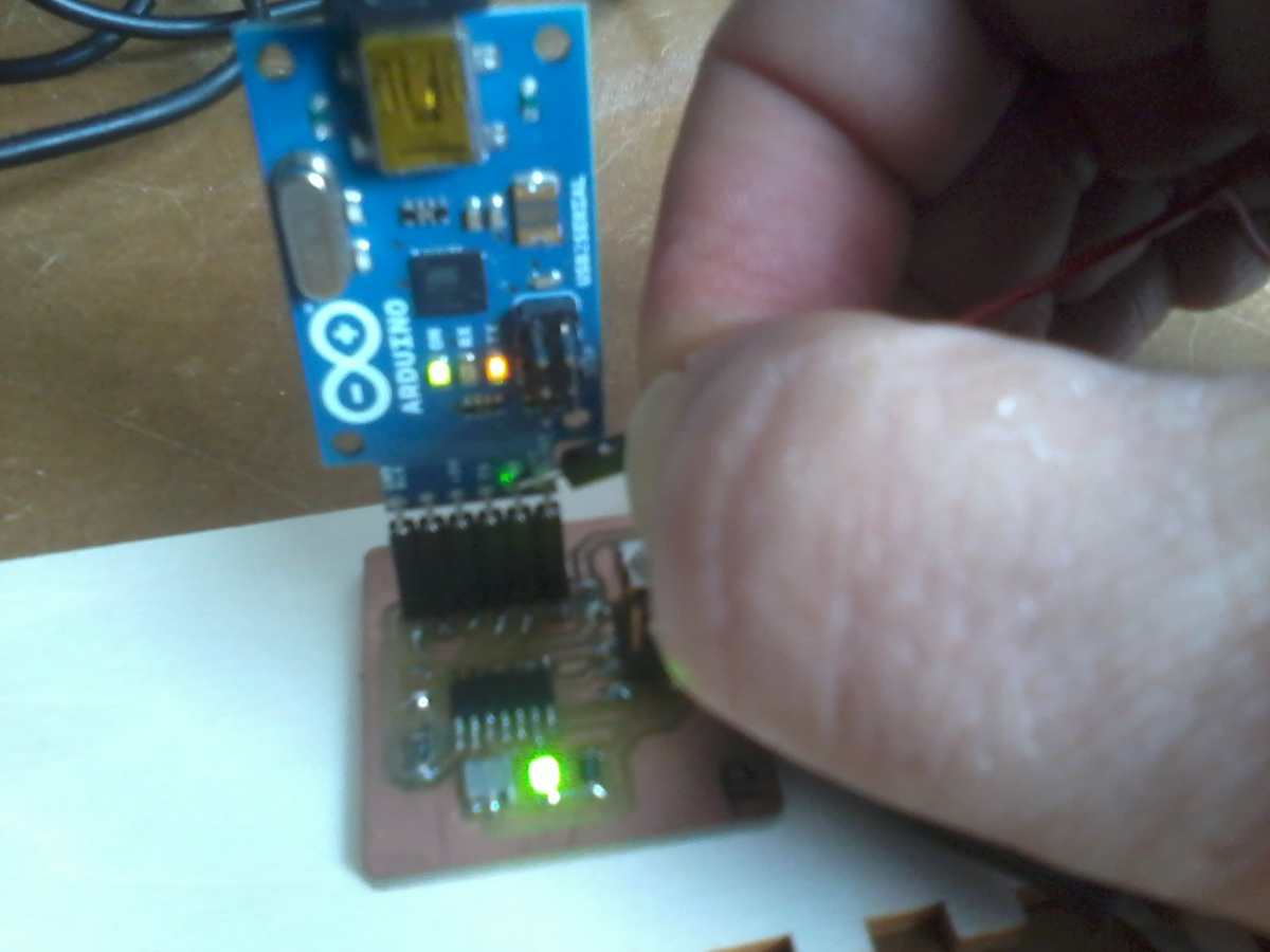
Hello world project
First, run Kicad and click  New project.
 First step : electronic schematic editor.
On this part, you choose components and define links between them.
Title, page size and orientation can be sets in  Page settings.
Type a key or use  to place a new component like ATtiny, Resonator, LED, Resistor.
You can move it with g, rotate it with r, change resistor value with v.
You can link pins with wires ( or w)
or put the same label (
or w)
or put the same label ( or l) on two different pins.
I couldn't find FTIheader, ISP connector and a switch with 4 pins. So, I made a library to create them.
 Second step : Library editor.
On this part, you can create or edit components.
Click on add component. Type Component name and Default reference designator.
Zomm in to see name and grid (to modify grid, click right and choos grid select).
Add pins to component ( or p) and set parameters. Most usefull are Pin name, Pin number and Orientation.
You can also add graphic lines to draw your component with  ,
,  or
or  .
.
At the end, save component to new library  or select working library
  and save it
library file exemple : FTDIheader
EESchema-LIBRARY Version 2.3
#encoding utf-8
#
# AVR-ISP-SMD
#
DEF AVR-ISP-SMD CONN 0 40 Y Y 1 F N
F0 "CONN" 0 -500 60 H V C CNN
F1 "AVR-ISP-SMD" 0 0 60 H V C CNN
F2 "" 0 0 60 H I C CNN
F3 "" 0 0 60 H I C CNN
DRAW
S -250 -100 250 -400 0 1 0 N
X MISO 1 -450 -150 200 R 50 50 1 1 I
X VCC 2 450 -150 200 L 50 50 1 1 I
X SCK 3 -450 -250 200 R 50 50 1 1 I
X MOSI 4 450 -250 200 L 50 50 1 1 I
X RST 5 -450 -350 200 R 50 50 1 1 I
X GND 6 450 -350 200 L 50 50 1 1 I
ENDDRAW
ENDDEF
Complete libray file
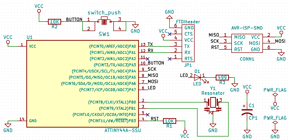
Hello world board schematic
When your schematic is finished, annotate your component  to give all a unique name like R1, R2, ...
Then check you schematic  .
.
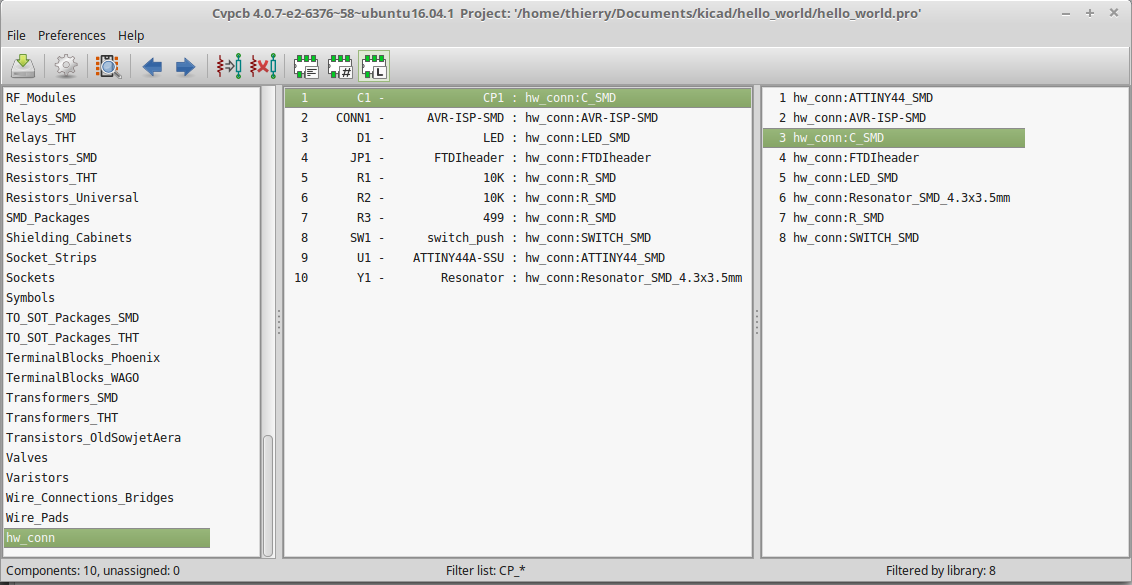
After, you have to associate logical component in schematic to footprint to be able to make your PCB.
If some are missing, you have to create them in the foot print editor  .
.
 Thirdstep : Footprint editor.
Select active library and then new Footprint .
Use pad settings  to define Pad type (SMD, ...) Shape (Rectangular, ...) and size.
Then place pads, change Pad number if necessary and save the footprint in the library . It will add each component in a .kicad_mod file in a .pretty folder.
C_SMD.kicad_mod
R_SMD.kicad_mod
FTDIheader.kicad_mod
SWITCH_SMD.kicad_mod
ATTINY44_SMD.kicad_mod
LED_SMD.kicad_mod
AVR-ISP-SMD.kicad_mod
Resonator_SMD_4.3x3.5mm.kicad_mod
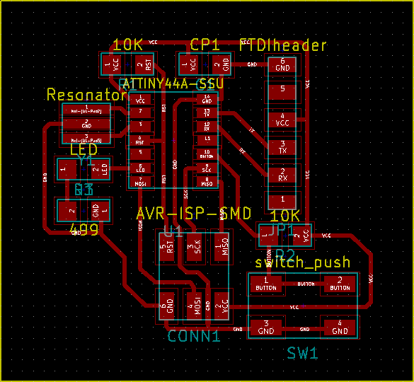
Hello world board netlist
When you finished to associate all components to footprint, generate netlist  and run Pcbnew
  .
.
 Fourth step : Pcbnew.
First read netlist . It will place foot prints and connection line between them.
Then, you have to design tracks  between pins on F.Cu laryer if you use SMD components and B.Cu layer for through hole components.
After, you can design board outline with add line and polygon  on Edge.Cuts layer.
At the end, export your PCB  .
.
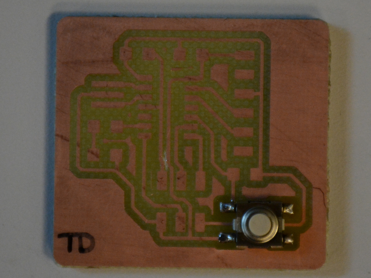
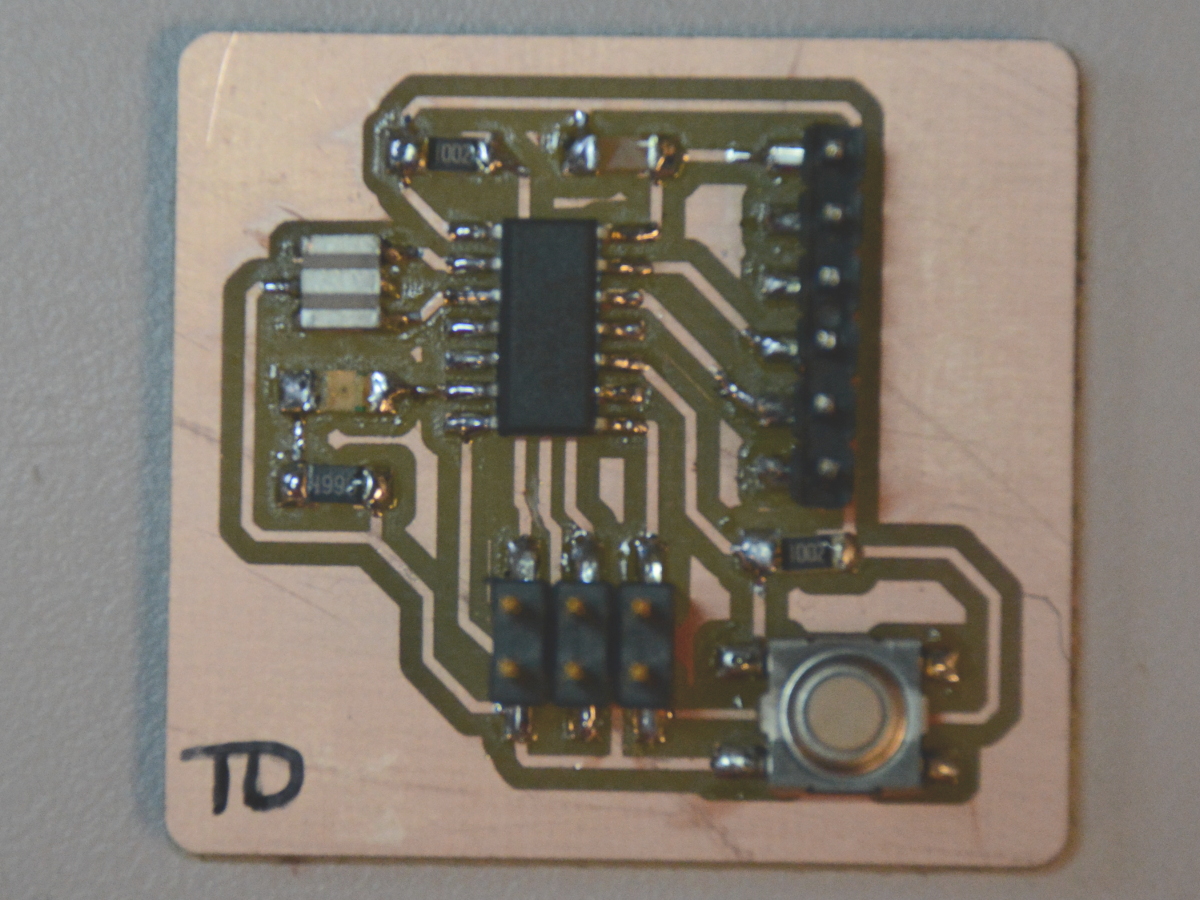
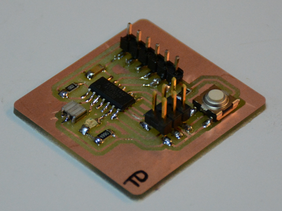
 I engrave my board using the