III. Designing a Sensor Board with KiCad
Because I was not satisfied with my previous Electronics design workflow, I decided to try out designing the sensor board in KiCad
I’ve some TCRT5000 compatible Reflective Optical Sensors in my tinkering box and it’s time now, to test these out.
Maybe I can use these also in my final project as wink gesture recognition.
I found a little nice tutorial about the sensor with a schematics for analog read
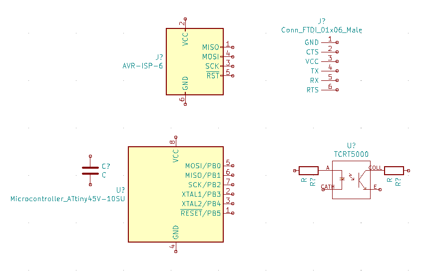
For the TCRT5000-Sensor Board the following parts are needed:
- 1x ATtiny45
- 1x TCRT5000
- 1x Resistor R100
- 1x Resistor 4K7
- 1x Resistor 1K (not shown in the screenshots!)
- 1x Resistor 10K (not shown in the screenshots!)
- 1x Capacitor 1.0 uF
- FTDI Pinheader
- ISP Pinheader
After milling I found out, that I missed two resistors. One 10kOhm connected from RST to VCC and one 1kOhm from PB2 to FTDI TX Pin. These are not shown in the following tutorial !!!
I got all my KiCad informations from the Aalto Fablab Youtube video Electronics Design with KiCAD
Thanks a lot Krisjanis for sharing your great lessons videos !!!
Installing KiCad
I don’t explain the installation process in detail. It’s well documented in the video above !
KiCad is available at it’s download page
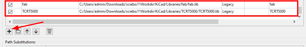
The KiCad fab library is available here
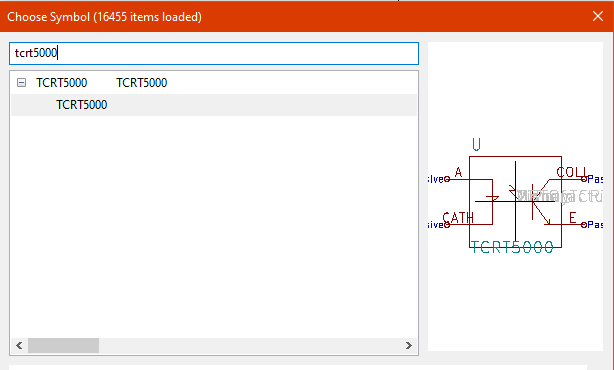
I got the needed TCRT5000 symbol and footprint from snapeda
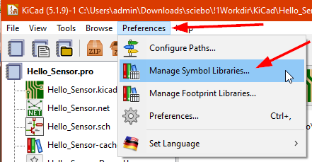
After installation and first of KiCad, the both Symbol Libraries has to be added
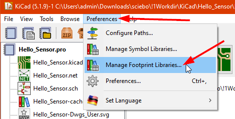
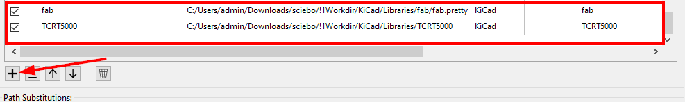
And the same with the Footprint Libraries
start drawing the schematics
My sensor board is based on the ATtiny45 version of this echo hello-world board
placing the symbols
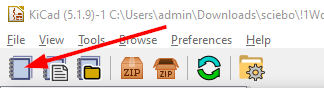
First we start with creating a new project.
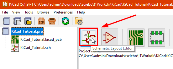
Then open the Schematics Layout Editor
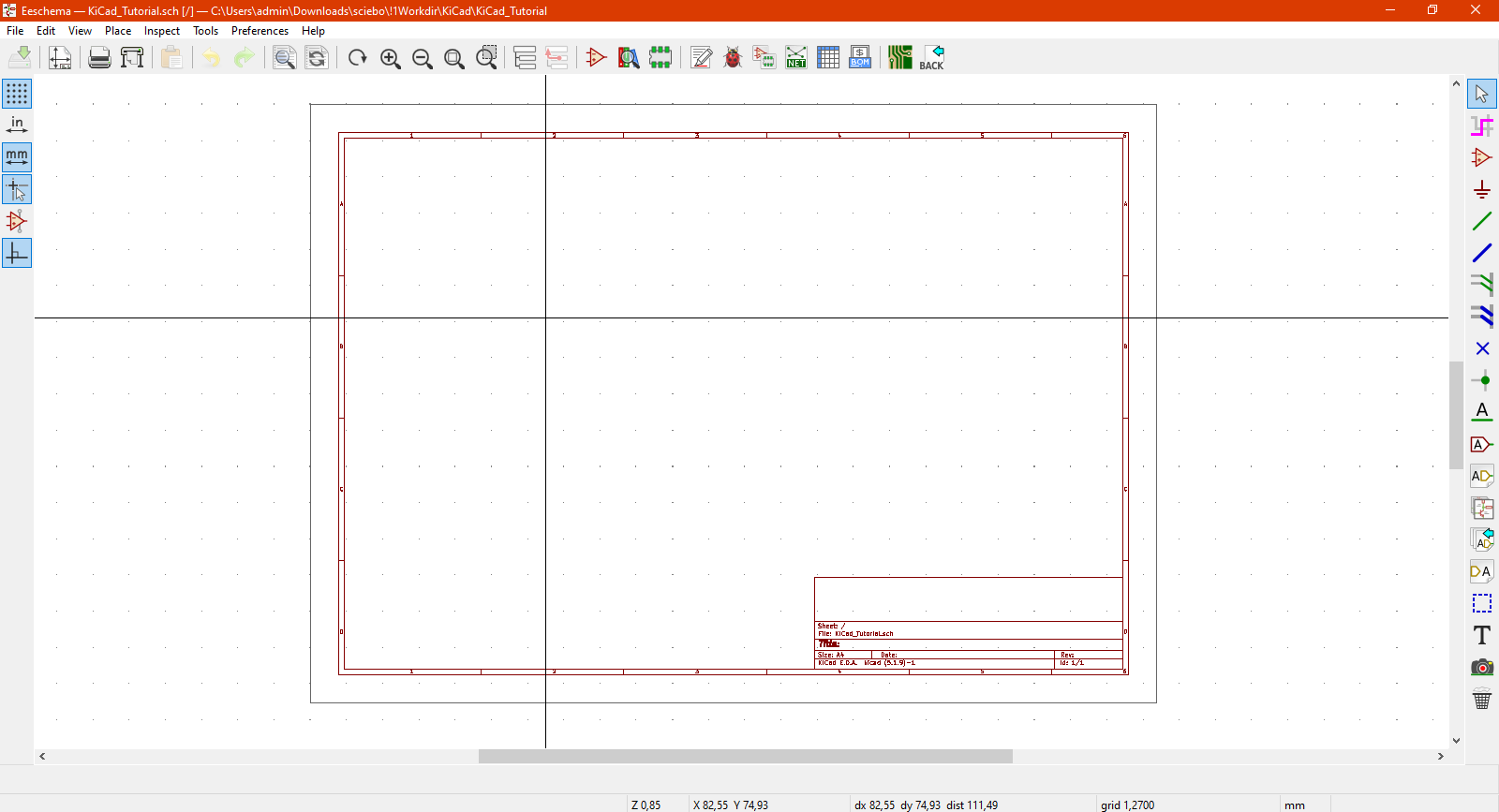
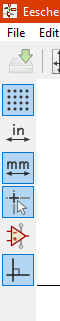
On the left side are some editing options like switching from mm to inches.
Here are the settings I activated
Start placing the parts with the Place Symbol icon on the right side
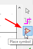
and then click somewhere, where the first part should be placed. A new window appears. There we can choose the Symbol (Electronical Part) we would like to place.
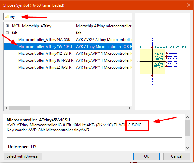
I start with the ATtiny45
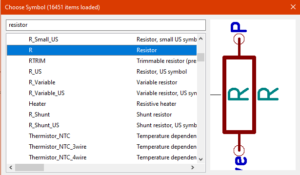
For the two resistors, it’s not necessary to choose a footprint. Just add the symbols
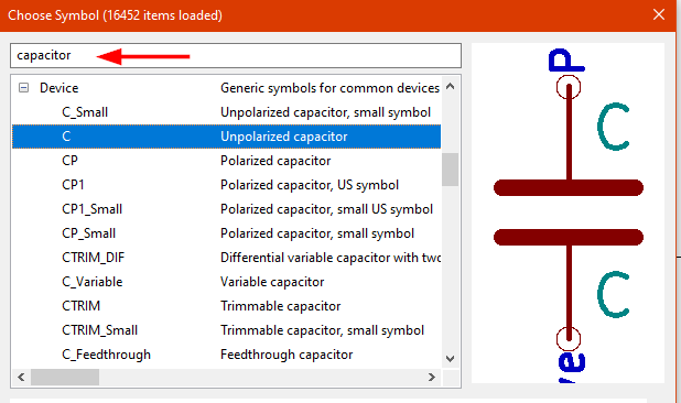
The ceramic capacitor is unpolarized and a footprint will be assigned later.
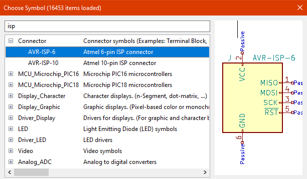
Next the 6 PIN ISP Header, again without footprint
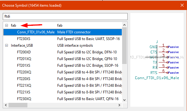
The FTDI Symbol we choose from the fab library
And at least the TCRT5000
arranging the symbols
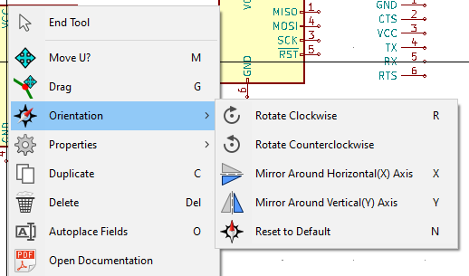
With a right click on a symbol, there are some editing options like move or rotate
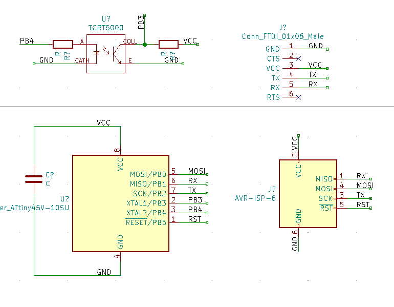
After arranging my schematics looks like this
connecting and wiring
The Symbols will be connected by drawing wires with the corresponding icon in the toolbar on the right side
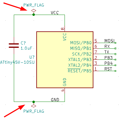
I connected just the capacitor directly by wires. On the output pins, I just draw a little wire. These can be placed with a double click, after drawing the line. These can be connected by placing labels on it, later.
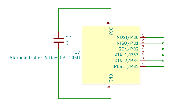
My schematics now looks like this
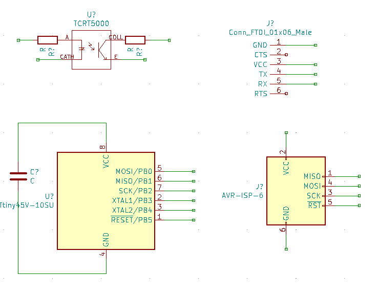
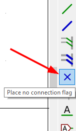
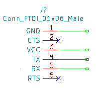
There are two connectors on the FTDI, which will not be used. To mark these pins as not connected, there is a flag that can be placed with the corresponding Icon
This is how the FTDI now looks like
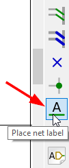
Now we place net labels
By clicking the corresponding wire. Here e.g. the VCC line.
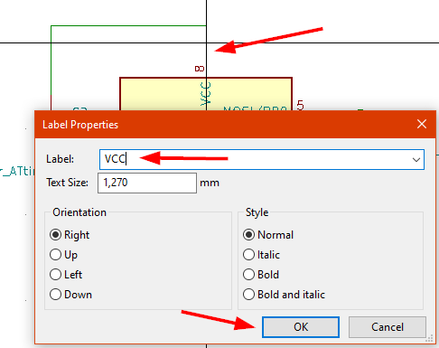
We go ahead with every connection we would like to make
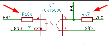
defining part values
With a right click on the resistors and the capacitor, it’s possible define their values
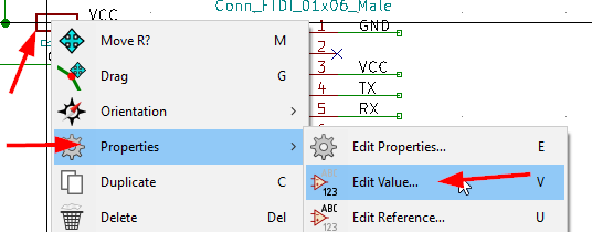
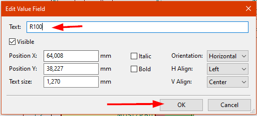
The Value labels are also rotate and movable
defining the power source
For passing the electrical rules check we have to set a power flag by placing a new symbol
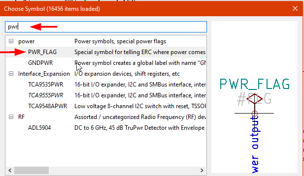
We need two of them. One for VCC and one for GND. These can be placed on any VCC and GND line.
Annotate schematics symbols
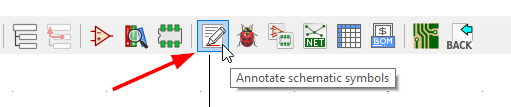
The next step is to annotate the schematics symbols by clicking the Icon in the top toolbar
We just confirm the dialog
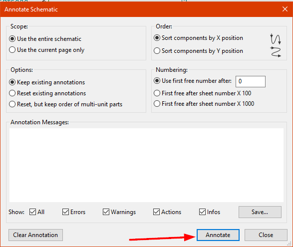
And I got the following annotation message:
Annotated PWR_FLAG as #FLG01
Annotated PWR_FLAG as #FLG02
Annotated 1.0uF as C1
Annotated Conn_FTDI_01x06_Male as J1
Annotated AVR-ISP-6 as J2
Annotated R100 as R1
Annotated 4K7 as R2
Annotated TCRT5000 as U1
Annotated Microcontroller_ATtiny45V-10SU as U2
Annotation complete.
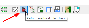
electrical rules check
Next step is the ERC by clicking the bug
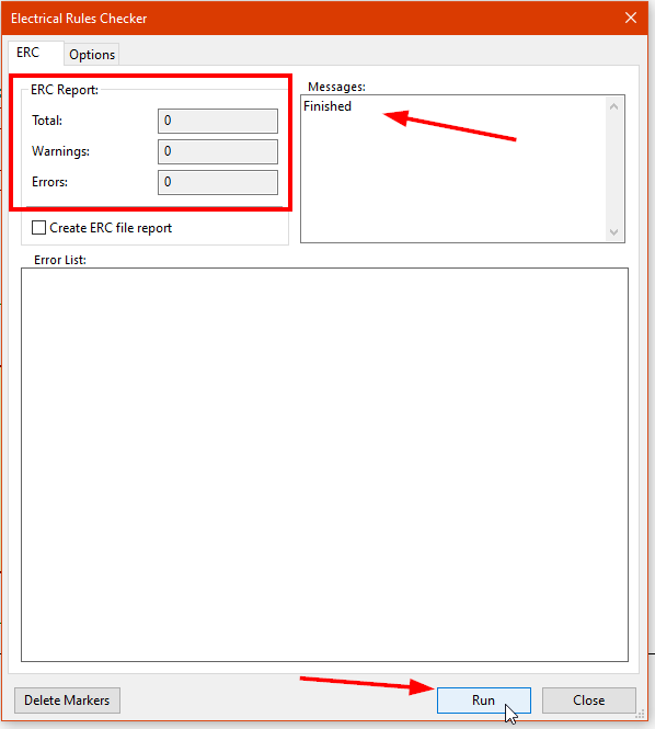
After running the test, there are no errors in my case
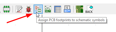
assinging the footprints
Now we have to assign the PCB footprints to the schematic symbols
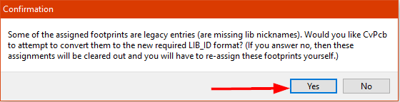
A message pops up. Just confirm with yes
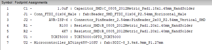
Now there is a list with the used components. Some of them have already an assigned footprint. The assigned footprint is behind the double-point.
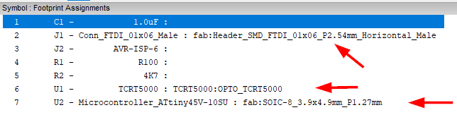
So the two resistors, the capacitor and the ISP Header have to be assigned.
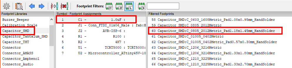
To do so, we click, in the middle list, on the part, which shall be assigned. I marked the C1- 1.0uFcapacitor for assigning.
In the left list, we choose the library we want to use. For the capacitor it is Capacitor_SMD
In the right list, are the filtered footprints. I’ve 0805 SMD Capacitors, so I chose corresponding footprint for hand soldering and cofirm with a double click on it.
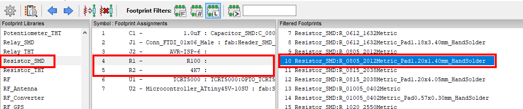
Now the same with the two resistors.
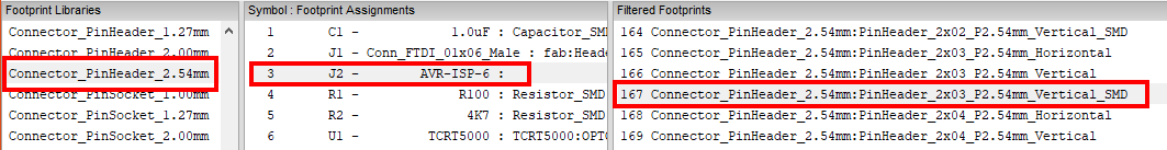
And the ISP Header
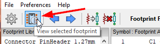
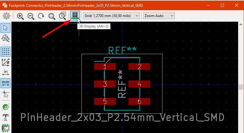
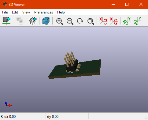
If it’s not clear, if the selected footprint is correct, there is an option to view it as an 3D animation.
After everything is done, the list should look like this
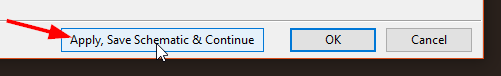
Now it is important to click Apply, Save Schematics & Continue and then confirm with ‘OK’
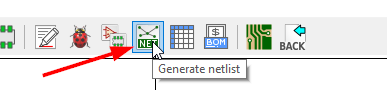
Generate Netlist
Now the Netlist has to be generate by clicking it’s icon and confirm the dialog
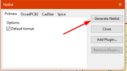
And just save it in the project folder
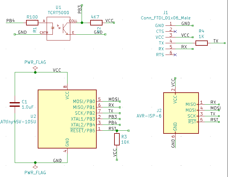
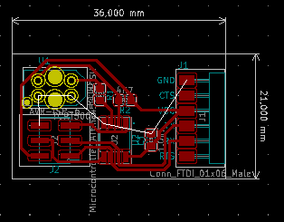
Updated schematics
This is the updated version of my schematics. The missing resistors are included now
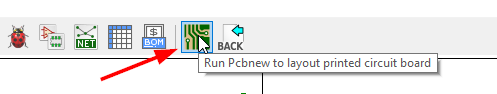
PCB Layout
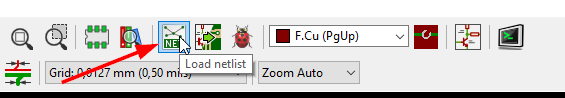
import the netlist
Now it’s time to switch to the PCB Layout Editor
and load the generated Netlist
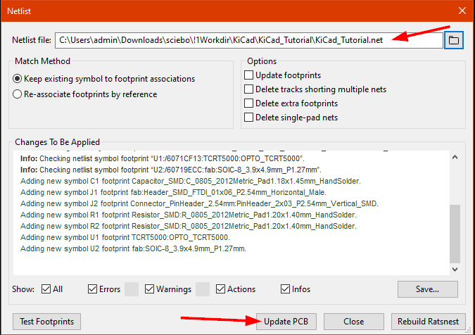
Just place the parts somewhere in the middle
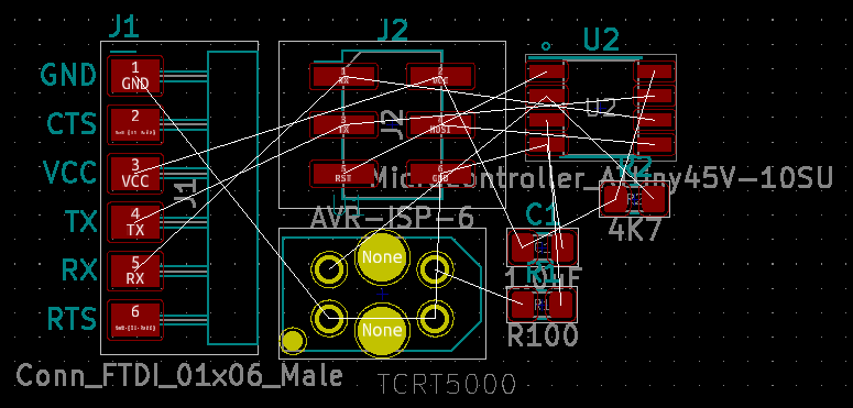
arranging the parts
Arranging the parts is similar to the schematics editor. Bring everything on it’s place.
First I changed the grid to 0.2mm

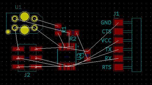
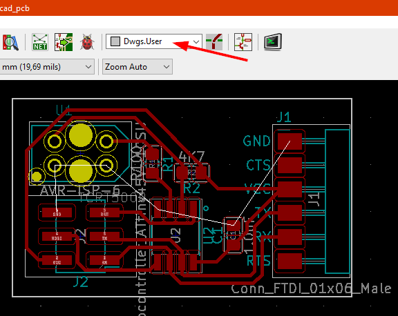
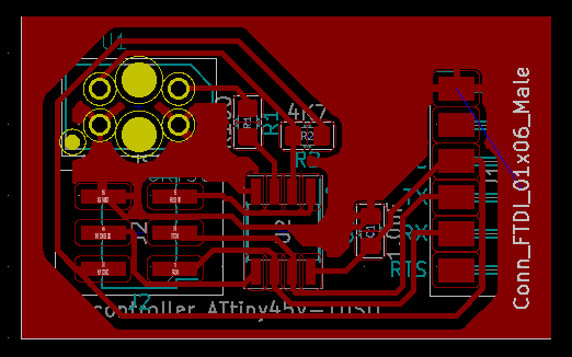
This is how I arranged them
modifying a footprint
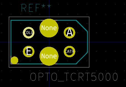
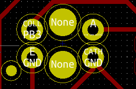
After milling I saw, that the solder pads from the TCRT5000 are to thin for hand soldering
To make the pads bigger, I selected the TCRT5000 and opened up the footprint editor
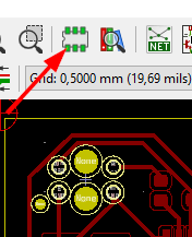
I made a double click on one of the pads.
And changed the Size X to 2 mm
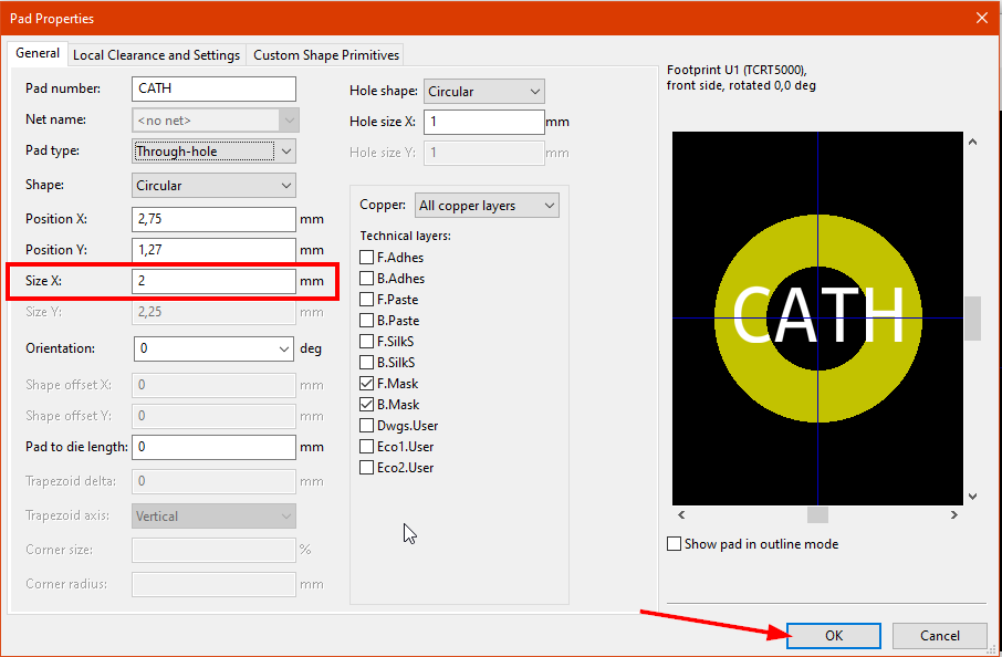
And did it for all four footprints.
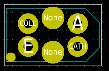
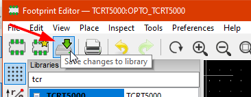
Afer changes made, just save and close the editor
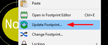
Back in the pcb layout editor, I made a right click on the TCRT5000 and hit Update Footprint...
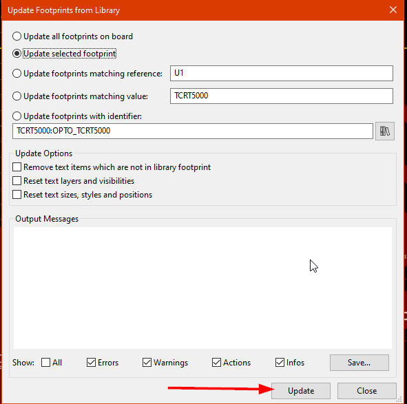
And confirmed the dialog with update
routing the tracks
Now let’s start routing the tracks.
For PCB milling, it’s better to adjust some design rules.
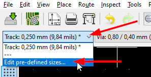
And edit the Net Classes
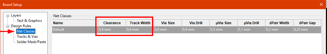
We change the values:
Clearance   -> 0.4mm
Track Width -> 0.4mm
Now we can start drawing the routs, but we leave the GND Pads open.
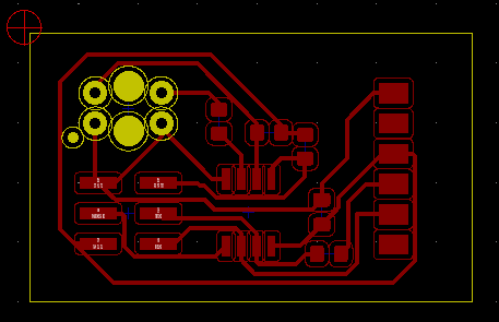
drawing the outline
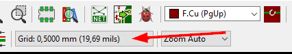
For drawing the outline, I changed the Grid to 0.5mm
The outline will be draw with the graphic lines tool
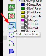
The lines are drawn automatically in the Dwgs.User layer
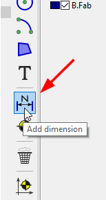
With the Add dimension Tool, we can check the size of the board
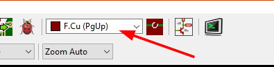
defining the GND Area
First we have to switch the layer back to F.Cu(PgUp)
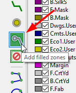
With the Add filled zones Tool, we can define the GND area.
After clicking on the first corner, a window pops-up and there we have to activate the /GND net and change some settings.
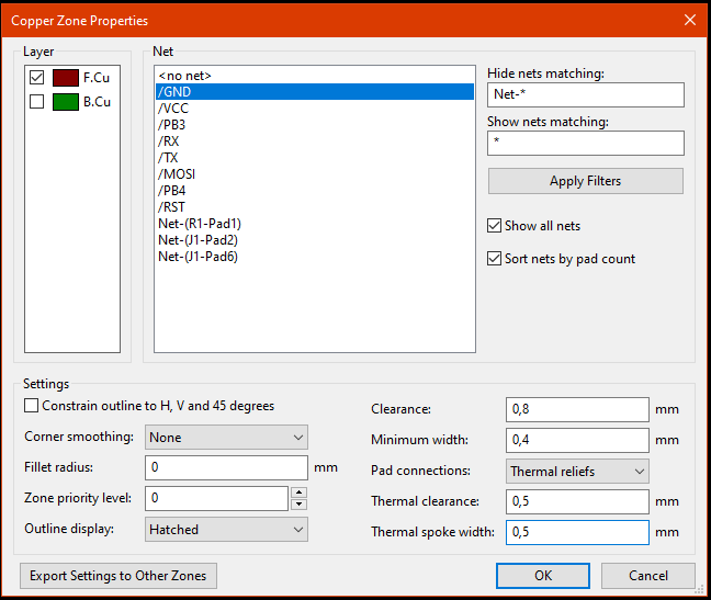
Clearance           -> 0,8 mm
Minimum Width       -> 0,4 mm
Thermal Clearance   -> 0,5 mm
Thermal spoke width -> 0,5 mm
After drawing the polygon around the pcb, the GND Area is generated.
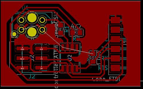
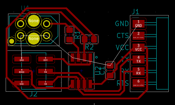
I don’t know why, but the GND lines from the TCRT5000 are not connected to ground, so I add a gnd route manually.
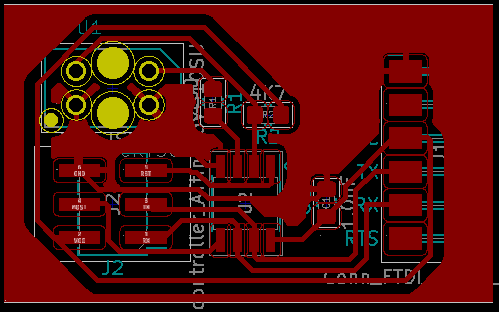
*** in my updated layout, I left the GND Area and routed the GND trace directly. This is how my updated pcb now looks like ***
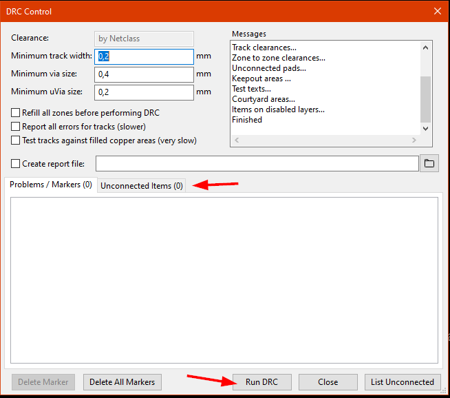
design rule check
Now we click again the bug icon for the design rule check and run the DRC
There are no errors found here
final steps
The dimensions added above have to be removed and there are some labels outside the board. We have to place them inside. I don’t know really why, at this moment.
preparing for mods
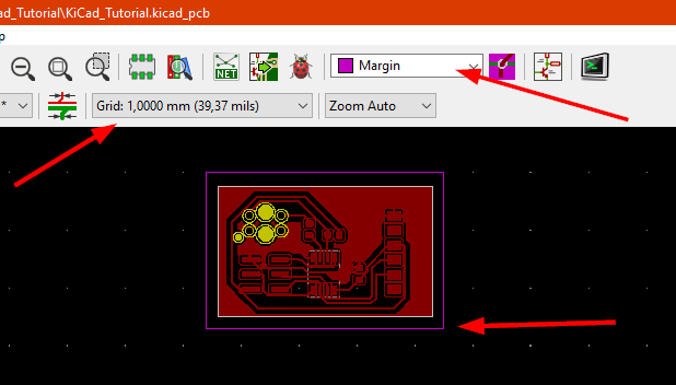
adding a margin
Now we need a margin around the board. Otherwise mods isn’t able to recognize the board outlines for cutting.
To do so, we have to change the layer to Margin and the grid to 1mm.
With the Add graphic lines tool, we draw now a margin around the board.
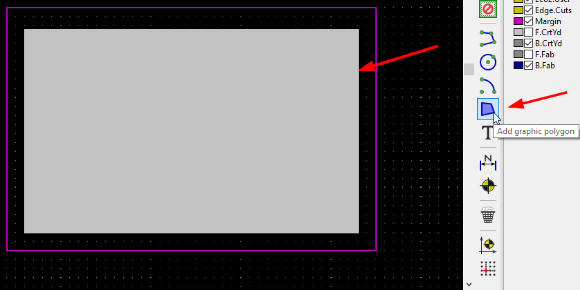
filled rectangle
We also need a filled a rectangle. To do so, the layer has to be changed to Dwgs.User and with the Add graphic polygon tool, we draw a polygon over the hole board
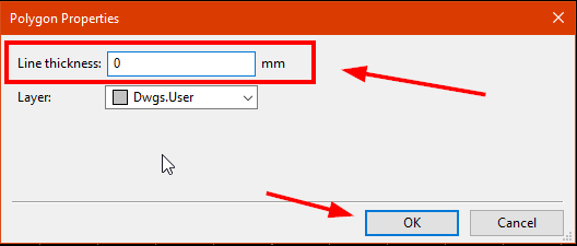
Then make a right click on the drawn polygon and choose Properties
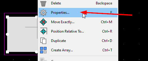
Change Line thickness to 0 and confirm with ‘OK’
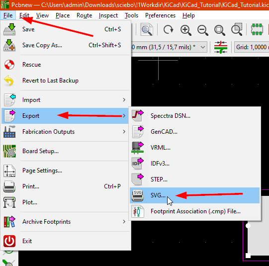
SVG Export
There we choose the options as shown in the following screenshot
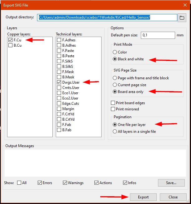
And after clicking the Export button, the svg files are generated.


preparing for FlatCAM
FlatCAM needs gerber files for generating the gcode. There are other preparations needed to export gerber files for FlatCAM.
adding Edge.Cuts
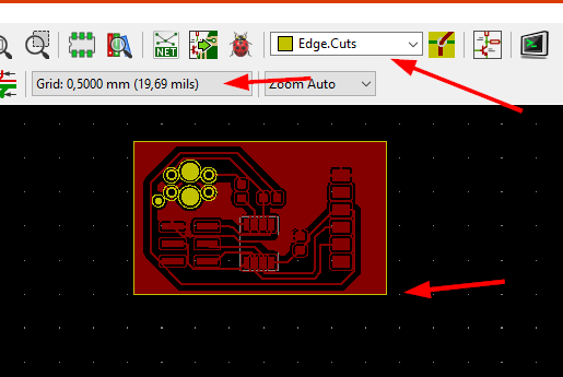
First I removed the filled rectangle, the outline and the margin. Then I changed the grid to 0.5mm, the layer to Edge.Cuts and draw, with the Add graphic lines tool, a square around the board.
define the origin
Then we have to define the x/y zero point by using the Placing the auxiliary axis origin Tool.
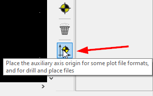
I placed it a bit above and left from the boards corner.

export the gerber files
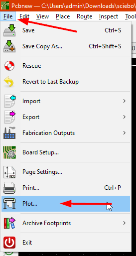
In the File - Plot menu, I used the following settings
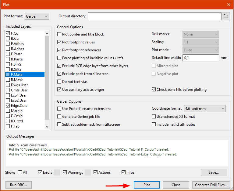
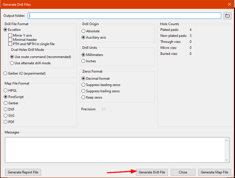
After push the Plot button, the gerber files are generated. In the same window, we have to push also the Generate Drill Files button
The gerber files are now generated and the KiCad part is finished.
Download
The ‘old’ Kicad Files with the generated svg’s and gerber files can be downloaded HERE
The ‘updated’ Kicad Files with the generated svg’s and gerber files can be downloaded HERE